ADC14L020
14-Bit, 20 MSPS, 150 mW A/D Converter
General Description
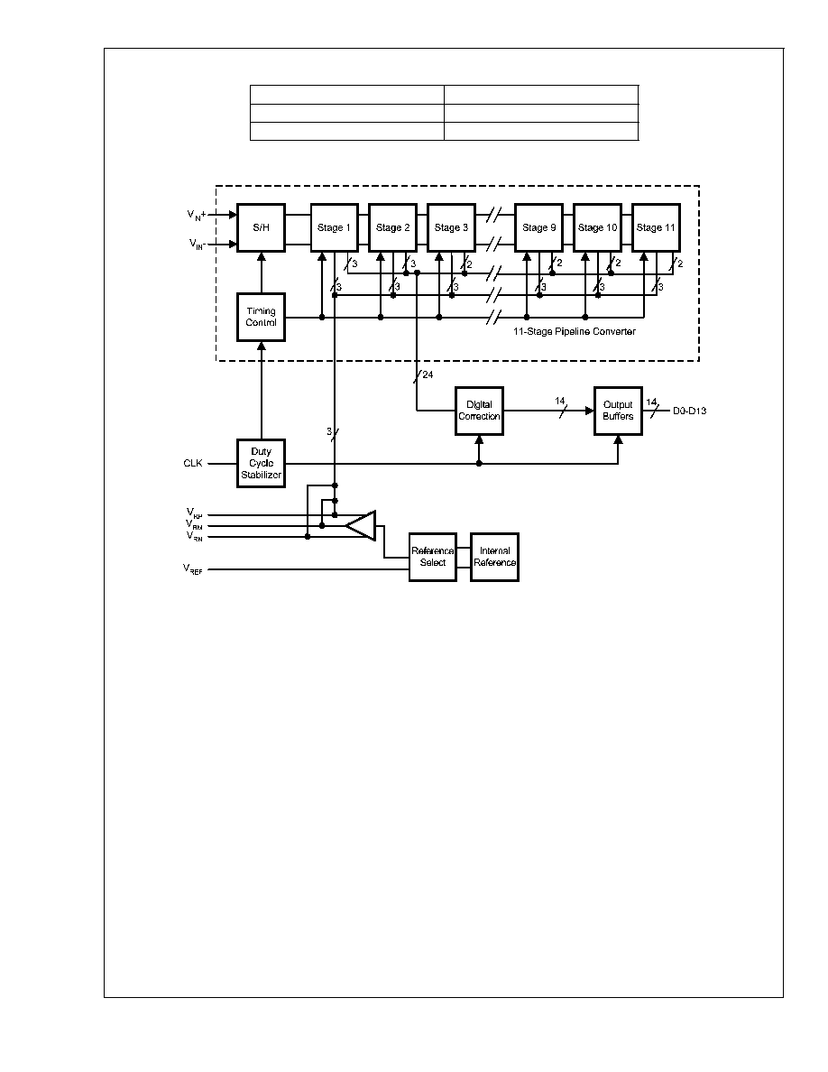
The ADC14L020 is a low power monolithic CMOS analog-
to-digital converter capable of converting analog input sig-
nals into 14-bit digital words at 20 Megasamples per second
(MSPS). This converter uses a differential, pipeline architec-
ture with digital error correction and an on-chip sample-and-
hold circuit to minimize power consumption while providing
excellent dynamic performance and a 150 MHz Full Power
Bandwidth. Operating on a single +3.3V power supply, the
ADC14L020 achieves 12.0 effective bits at nyquist and con-
sumes just 150 mW at 20 MSPS . The Power Down feature
reduces power consumption to 15 mW.
The differential inputs provide a full scale differential input
swing equal to 2 times V
REF
with the possibility of a single-
ended input. Full use of the differential input is recom-
mended for optimum performance. Duty cycle stabilization
and output data format are selectable using a quad state
function pin. The output data can be set for offset binary or
two's complement.
To ease interfacing to lower voltage systems, the digital
output driver power pins of the ADC14L020 can be con-
nected to a separate supply voltage in the range of 2.4V to
the analog supply voltage.
This device is available in the 32-lead LQFP package and
will operate over the industrial temperature range of -40∞C to
+85∞C. An evaluation board is available to ease the evalua-
tion process.
Features
n
Single +3.3V supply operation
n
Internal sample-and-hold
n
Internal reference
n
Outputs 2.4V to 3.6V compatible
n
Duty Cycle Stabilizer
n
Power down mode
Key Specifications
n
Resolution
14 Bits
n
DNL
±
0.5 LSB (typ)
n
SNR (f
IN
= 10 MHz)
74 dB (typ)
n
SFDR (f
IN
= 10 MHz)
93 dB (typ)
n
Data Latency
7 Clock Cycles
n
Power Consumption
n
-- Operating
150 mW (typ)
n
-- Power Down Mode
15 mW (typ)
Applications
n
Medical Imaging
n
Instrumentation
n
Communications
n
Digital Video
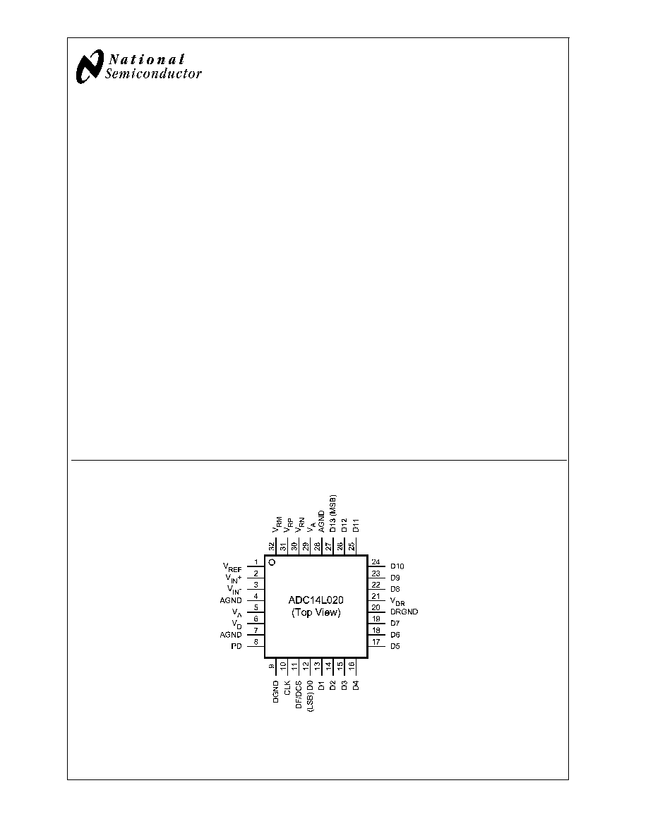
Connection Diagram
20157001
August 2005
ADC14L020
14-Bit,
20
MSPS,
150
mW
A/D
Converter
© 2005 National Semiconductor Corporation
DS201570
www.national.com
Ordering Information
Industrial (-40∞C
T
A
+85∞C)
Package
ADC14L020CIVY
32 Pin LQFP
ADC14L020EVAL
Evaluation Board
Block Diagram
20157002
ADC14L020
www.national.com
2

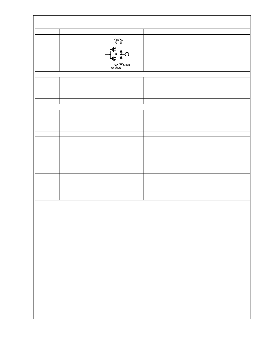
Pin Descriptions and Equivalent Circuits
Pin No.
Symbol
Equivalent Circuit
Description
ANALOG I/O
2
V
IN
+
Differential analog input pins. With a 1.0V reference voltage the
differential full-scale input signal level is 2.0 V
P-P
with each
input pin voltage centered on a common mode voltage, V
CM
.
The negative input pins may be connected to V
CM
for
single-ended operation, but a differential input signal is
required for best performance.
3
V
IN
-
1
V
REF
This pin is the reference select pin and the external reference
input.
If (V
A
- 0.3V)
<
V
REF
<
V
A
, the internal 1.0V reference is
selected.
If AGND
<
V
REF
<
(AGND + 0.3V), the internal 0.5V reference
is selected.
If a voltage in the range of 0.4V to (V
A
- 0.4V) is applied to this
pin, that voltage is used as the reference.
The full scale differential voltage range is 2 * V
REF
. V
REF
should be bypassed to AGND with a 0.1 µF capacitor when an
external reference is used.
31
V
RP
These pins should each be bypassed to AGND with a low ESL
(equivalent series inductance) 0.1 µF capacitor. A 10 µF
capacitor should be placed between the V
RP
and V
RN
.
V
RM
may be loaded to 1mA for use as a temperature stable
1.5V reference. The remaining pins should not be loaded.
V
RM
may be used to provide the common mode voltage, V
CM
,
for the differential inputs.
32
V
RM
31
V
RN
11
DF/DCS
This is a four-state pin.
DF/DCS = V
A
, output data format is offset binary with duty
cycle stabilization applied to the input clock
DF/DCS = AGND, output data format is 2's complement, with
duty cycle stabilization applied to the input clock.
DF/DCS = V
RM
, output data is 2's complement without duty
cycle stabilization applied to the input clock
DF/DCS = "float", output data is offset binary without duty cycle
stabilization applied to the input clock.
DIGITAL I/O
10
CLK
Digital clock input. The range of frequencies for this input is as
specified in the electrical tables with guaranteed performance
at 20 MHz. The input is sampled on the rising edge.
8
PD
PD is the Power Down input pin. When high, this input puts the
converter into the power down mode. When this pin is low, the
converter is in the active mode.
ADC14L020
www.national.com
3
Pin Descriptions and Equivalent Circuits
(Continued)
Pin No.
Symbol
Equivalent Circuit
Description
12-19
22-27
D0≠D13
Digital data output pins that make up the 14-bit conversion
result. D0 (pin 12) is the LSB, while D13 (pin 27) is the MSB of
the output word. Output levels are TTL/CMOS compatible.
Optimum loading is
<
10pF.
ANALOG POWER
5, 29
V
A
Positive analog supply pins. These pins should be connected
to a quiet +3.3V source and bypassed to AGND with 0.1 µF
capacitors located close to these power pins, and with a 10 µF
capacitor.
4, 7
AGND
The ground return for the analog supply.
DIGITAL POWER
6
V
D
Positive digital supply pin. This pin should be connected to the
same quiet +3.3V source as is V
A
and be bypassed to DGND
with a 0.1 µF capacitor located close to the power pin and with
a 10 µF capacitor.
9
DGND
The ground return for the digital supply.
21
V
DR
Positive driver supply pin for the ADC14L020's output drivers.
This pin should be connected to a voltage source of +2.4V to
V
D
and be bypassed to DR GND with a 0.1 µF capacitor. If the
supply for this pin is different from the supply used for V
A
and
V
D
, it should also be bypassed with a 10 µF capacitor. V
DR
should never exceed the voltage on V
D
. All 0.1 µF bypass
capacitors should be located close to the supply pin.
20
DR GND
The ground return for the digital supply for the ADC's output
drivers. These pins should be connected to the system digital
ground, but not be connected in close proximity to the ADC's
DGND or AGND pins. See Section 5 (Layout and Grounding)
for more details.
ADC14L020
www.national.com
4
Absolute Maximum Ratings
(Notes 1,
2)
If Military/Aerospace specified devices are required,
please contact the National Semiconductor Sales Office/
Distributors for availability and specifications.
V
A
, V
D
, V
DR
4.2V
|V
A
≠V
D
|
100 mV
Voltage on Any Input or Output Pin
-0.3V to (V
A
or V
D
+0.3V)
Input Current at Any Pin (Note 3)
±
25 mA
Package Input Current (Note 3)
±
50 mA
Package Dissipation at T
A
= 25∞C
See (Note 4)
ESD Susceptibility
Human Body Model (Note 5)
2500V
Machine Model (Note 5)
250V
Storage Temperature
-65∞C to +150∞C
Soldering process must comply with National
Semiconductor's Reflow Temperature Profile
specifications. Refer to www.national.com/packaging.
(Note 6)
Operating Ratings
(Notes 1, 2)
Operating Temperature
-40∞C
T
A
+85∞C
Supply Voltage (V
A
, V
D
)
+3.0V to +3.6V
Output Driver Supply (V
DR
)
+2.4V to V
D
CLK, PD
-0.05V to (V
D
+ 0.05V)
Clock Duty Cycle (DCS On)
20% to 80%
Clock Duty Cycle (DCS Off)
40% to 60%
Analog Input Pins
0V to 2.6V
V
CM
0.5V to 2.0V
|AGND≠DGND|
100mV
Converter Electrical Characteristics
Unless otherwise specified, the following specifications apply for AGND = DGND = DR GND = 0V, V
A
= V
D
= +3.3V, V
DR
=
+2.5V, PD = 0V, External V
REF
= +1.0V, f
CLK
= 20 MHz, f
IN
= 10 MHz at -0.5dBFS, t
r
= t
f
= 2 ns, C
L
= 15 pF/pin, Duty Cycle
Stabilizer On. Boldface limits apply for T
J
= T
MIN
to T
MAX
: all other limits T
J
= 25∞C (Notes 7, 8, 9)
Symbol
Parameter
Conditions
Typical
(Note 10)
Limits
(Note 10)
Units
(Limits)
STATIC CONVERTER CHARACTERISTICS
Resolution with No Missing Codes
14
Bits (min)
INL
Integral Non Linearity (Note 11)
±
1.4
±
3.8
LSB (max)
DNL
Differential Non Linearity
±
0.5
±
1.0
LSB (max)
PGE
Positive Gain Error
0.3
±
3.3
%FS (max)
NGE
Negative Gain Error
0.3
±
3.3
%FS (max)
TC GE
Gain Error Tempco
-40∞C
T
A
+85∞C
2.5
ppm/∞C
V
OFF
Offset Error (V
IN
+ = V
IN
-)
-0.06
±
0.85
%FS (max)
TC
V
OFF
Offset Error Tempco
-40∞C
T
A
+85∞C
1.5
ppm/∞C
Under Range Output Code
0
Over Range Output Code
16383
REFERENCE AND ANALOG INPUT CHARACTERISTICS
V
CM
Common Mode Input Voltage
1.5
0.5
V (min)
2.0
V (max)
V
RM
Reference Output Voltage
Output load = 1 mA
1.5
V
C
IN
V
IN
Input Capacitance (each pin to
GND)
V
IN
= 1.5 Vdc
±
0.5 V
(CLK LOW)
11
pF
(CLK HIGH)
4.5
pF
V
REF
External Reference Voltage (Note
13)
1.00
0.8
V (min)
1.2
V (max)
Reference Input Resistance
1
M
(min)
ADC14L020
www.national.com
5