ADC16061
Self-Calibrating 16-Bit, 2.5 MSPS, 390 mW A/D Converter
General Description
The ADC16061 is a self-calibrating 16-bit, 2.5 Megasample
per second analog to digital converter. It operates on a single
+5V supply, consuming just 390mW (typical).
The ADC16061 provides an easy and affordable upgrade
from 12 bit and 14 bit converters. The ADC16061 may also
be used to replace many hybrid converters with a resultant
saving of space, power and cost.
The ADC16061 operates with excellent dynamic perfor-
mance at input frequencies up to
1
/
2
the clock frequency. The
calibration feature of the ADC16061 can be used to get more
consistent and repeatable results over the entire operating
temperature range. On-command self-calibration reduces
many of the effects of temperature-induced drift, resulting in
more repeatable conversions.
The Power Down feature reduces power consumption to
less than 2mW.
The ADC16061 comes in a TQFP and is designed to operate
over the commercial temperature range of 0∞C to +70∞C.
Features
n
Single +5V Operation
n
Self Calibration
n
Power Down Mode
Key Specifications
n
Resolution
16 Bits
n
Conversion Rate
2.5 Msps (min)
n
DNL
1.0 LSB (typ)
n
SNR (f
IN
= 500 kHz)
80 dB (typ)
n
Supply Voltage
+5V
±
5%
n
Power Consumption
390mW (typ)
Applications
n
PC-Based Data Acquisition
n
Document Scanners
n
Digital Copiers
n
Film Scanners
n
Blood Analyzers
n
Sonar/Radar
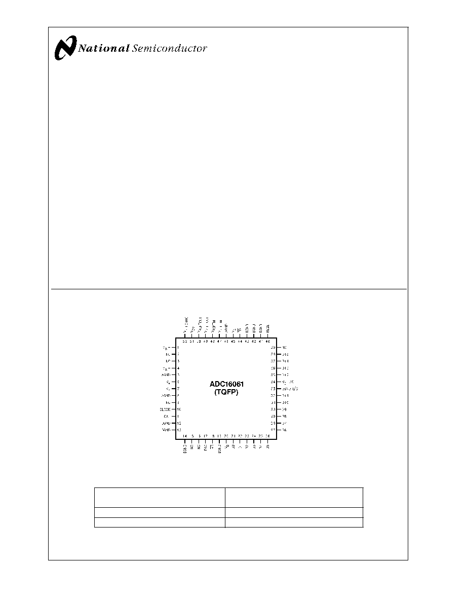
Connection Diagram
10088901
Ordering Information
Commercial
(0∞C
TA
+70∞C)
Package
ADC16061CCVT
VEG52A 52 Pin Thin Quad Flat Pack
ADC16061EVAL
Evaluation Board
December 2001
ADC16061
Self-Calibrating
16-Bit,
2.5
MSPS,
390
mW
A/D
Converter
© 2001 National Semiconductor Corporation
DS100889
www.national.com
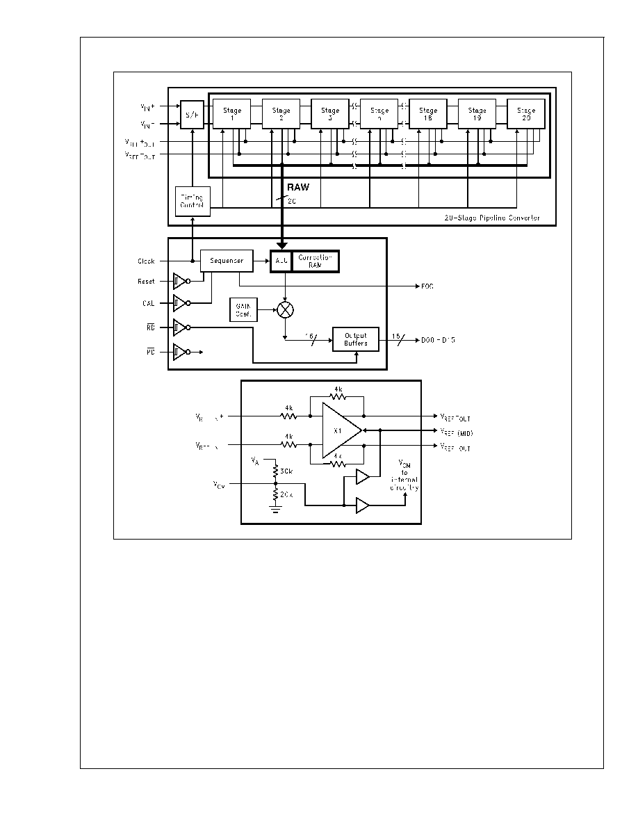
Block Diagram
10088902
ADC16061
www.national.com
2
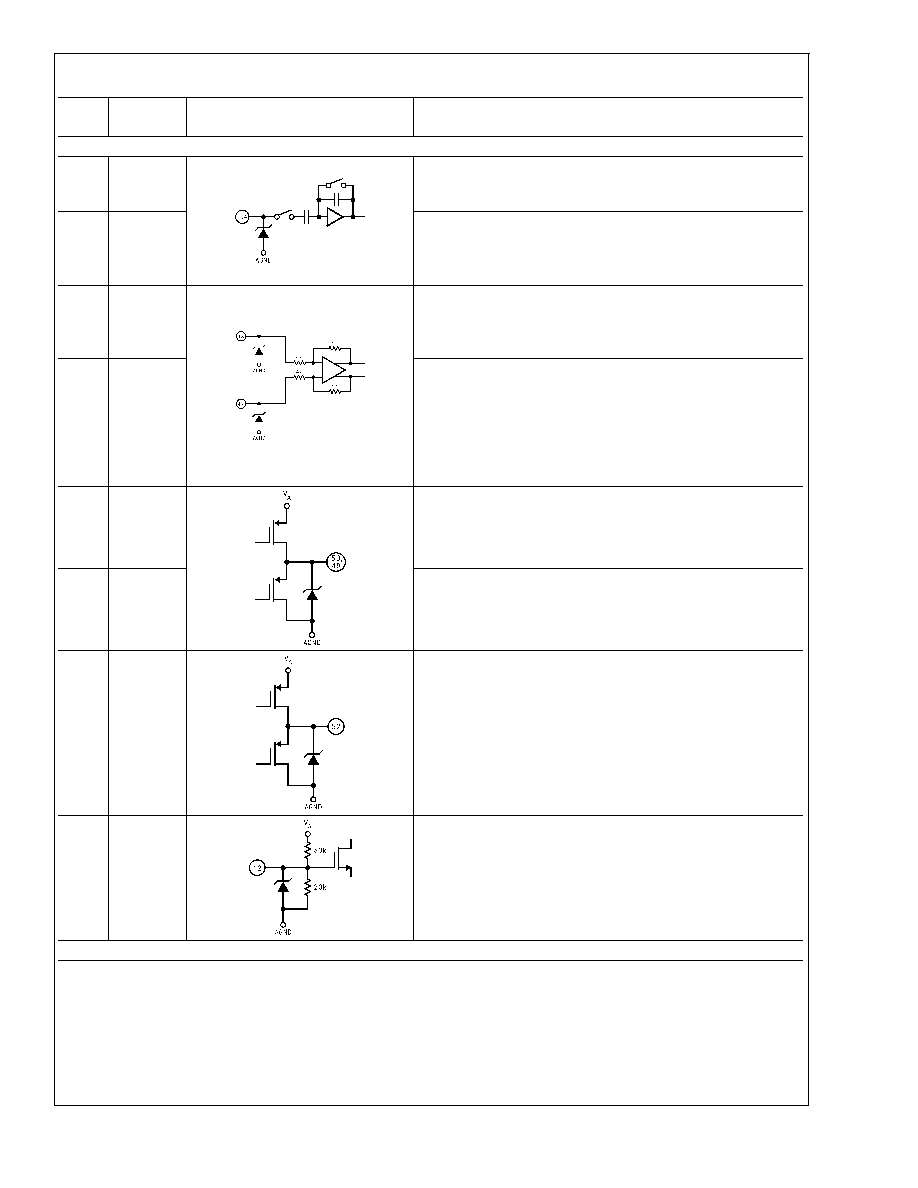
Pin Descriptions and Equivalent Circuits
Pin
No.
Symbol
Equivalent Circuit
Description
Analog I/O
1
V
IN
+
Non-Inverting analog signal Input. With a 2.0V reference voltage
and a 2.0V common mode voltage, V
CM
, the input signal voltage
range is from 1.0 volt to 3.0 Volts.
4
V
IN
-
Inverting analog signal Input. With a 2.0V reference voltage and a
2.0V common mode voltage, V
CM
, the input signal voltage range is
from 1.0 Volt to 3.0 Volts. The input signal should be balanced for
best performance.
48
V
REF
+
IN
Positive reference input. This pin should be bypassed to AGND
with a 0.1 µF monolithic capacitor. V
REF
+ minus V
REF- IN
should be
a minimum of 1.8V and a maximum of 2.2V. The full-scale input
voltage is equal to V
REF
+
IN
minus V
REF
-
IN
.
47
V
REF
-
IN
Negative reference input. In most applications this pin should be
connected to AGND and the full reference voltage applied to V
REF
+
IN
. If the application requires that V
REF
-
IN
be offset from AGND,
this pin should be bypassed to AGND with a 0.1 µF monolithic
capacitor. V
REF
+
IN
minus V
REF- IN
should be a minimum of 1.8V
and a maximum of 2.2V. The full-scale input voltage is equal to
V
REF
+
IN
minus V
REF
-
IN
.
50
V
REF
+
OUT
Output of the high impedance positive reference buffer. With a
2.0V reference input, and with a V
CM
of 2.0V, this pin will have a
3.0V output voltage. This pin should be bypassed to AGND with a
0.1 µF monolithic capacitor in parallel with a 10 µF capacitor.
49
V
REF
-
OUT
The output of the negative reference buffer. With a 2.0V reference
and a V
CM
of 2.0V, this pin will have a 1.0V output voltage. This
pin should be bypassed to AGND with a 0.1 µF monolithic
capacitor in parallel with a 10 µF capacitor.
52
V
REF (MID)
Output of the reference mid-point, nominally equal to 0.4 V
A
(2.0V).
This pin should be bypassed to AGND with a 0.1 µF monolithic
capacitor. This voltage is derived from V
CM
.
51
V
CM
Input to the common mode buffer, nominally equal to 40% of the
supply voltage (2.0V). This pin should be bypassed to AGND with
a 0.1 µF monolithic capacitor. Best performance is obtained if this
pin is driven with a low impedance source of 2.0V.
Digital I/O
ADC16061
www.national.com
3
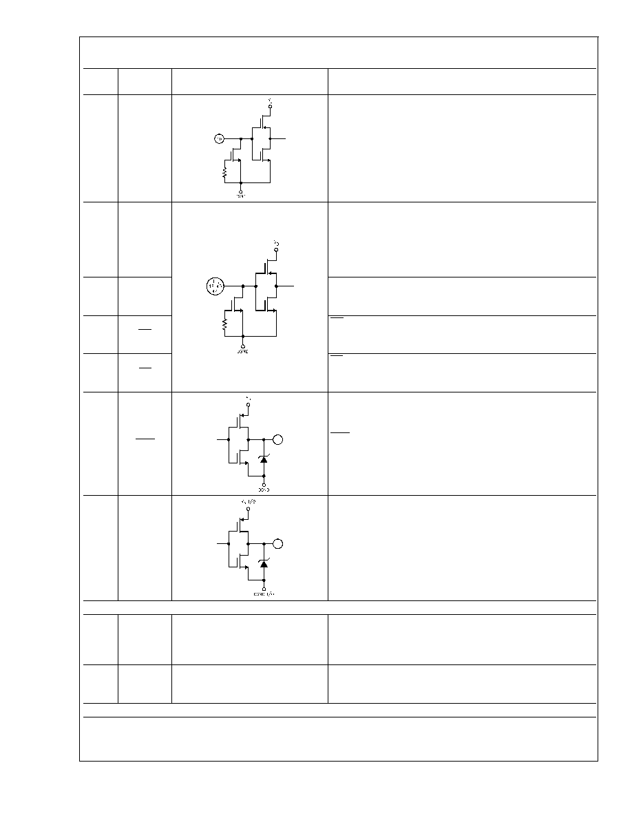
Pin Descriptions and Equivalent Circuits
(Continued)
Pin
No.
Symbol
Equivalent Circuit
Description
10
CLOCK
Digital clock input. The input voltage is captured t
AD
after the fall of
the clock signal. The range of frequencies for this input is 300 kHz
to 2.5 MHz. The clock frequency should not be changed or
interrupted during conversion or while reading data output.
11
CAL
CAL is a level-sensitive digital input that, when pulsed high for at
least two clock cycles, puts the ADC into the CALIBRATE mode.
Calibration should be performed upon ADC power-up (after
asserting a reset) and each time the temperature changes by more
than 50∞C since the ADC16061 was last calibrated. See Section
2.3 for more information.
40
RESET
RESET is a level-sensitive digital input that, when pulsed high for
at least 2 CLOCK cycles, results in the resetting of the ADC. This
reset pulse must be applied after ADC power-up, before calibration.
18
RD
RD is the (READ) digital input that, when low, enables the output
data buffers. When this input pin is high, the output data bus is in a
high impedance state.
44
PD
PD is the Power Down input that, when low, puts the converter into
the power down mode. When this pin is high, the converter is in
the active mode.
17
EOC
EOC is a digital output that, when low, indicates the availability of
new conversion results at the data output pins.
21-32
35-38
D00-15
Digital data outputs that make up the 16-bit TRI-STATE conversion
results. D00 is the LSB, while D15 is the MSB (SIGN bit) of the
two's complement output word.
Analog Power
6, 7, 45
V
A
Positive analog supply pins. These pins should be connected to a
clean, quiet +5V source and bypassed to AGND with 0.1 µF
monolithic capacitors in parallel with 10 µF capacitors, both located
within 1 cm of these power pins.
5, 8, 46
AGND
The ground return for the analog supply. AGND and DGND should
be connected together directly beneath the ADC16061 package.
See Section 5 (Layout and grounding) for more details).
Digital Power
ADC16061
www.national.com
4

Pin Descriptions and Equivalent Circuits
(Continued)
Pin
No.
Symbol
Equivalent Circuit
Description
20
V
D
Positive digital supply pin. This pin should be connected to the
same clean, quiet +5V source as is V
A
and bypassed to DGND
with a 0.1 µF monolithic capacitor in parallel with a 10µF capacitor,
both located within 1 cm of the power pin.
12, 13,
14, 19,
41, 42,
43
DGND
The ground return for the digital supply. AGND and DGND should
be connected together directly beneath the ADC16061 package.
See Section 5 (Layout and Grounding) for more details.
34
V
D
I/O
Positive digital supply pin for the ADC16061's output drivers. This
pin should be connected to a +3V to +5V source and bypassed to
DGND I/O with a 0.1 µF monolithic capacitor. If the supply for this
pin is different from the supply used for V
A
and V
D
, it should also
be bypassed with a 10 µF capacitor. All bypass capacitors should
be located within 1 cm of the supply pin.
33
DGND I/O
The ground return for the digital supply for the ADC16061's output
drivers. This pin should be connected to the system digital ground,
but not be connected in close proximity to the ADC16061's DGND
or AGND pins. See Section 5.0 (Layout and Grounding) for more
details.
NC
2, 3, 9,
15, 16,
39
NC
All pins marked NC (no connect) should be left floating. Do not
connect the NC pins to ground, power supplies, or any other
potential or signal. These pins are used for test in the
manufacturing process.
ADC16061
www.national.com
5