 | –≠–ª–µ–∫—Ç—Ä–æ–Ω–Ω—ã–π –∫–æ–º–ø–æ–Ω–µ–Ω—Ç: C397 | –°–∫–∞—á–∞—Ç—å:  PDF PDF  ZIP ZIP |
LM397
Single General Purpose Voltage Comparator
General Description
The LM397 is a single voltage comparator with an input
common mode that includes ground. The LM397 is designed
to operate from a single 5V to 30V power supply or a split
power supply. Its low supply current is virtually independent
of the magnitude of the supply voltage.
The LM397 features an open collector output stage. This
allows the connection of an external resistor at the output.
The output can directly interface with TTL, CMOS and other
logic levels, by tying the resistor to different voltage levels
(level translator).
The LM397 is available in space saving SOT23-5 package
and pin compatible to TI's TL331, single differential com-
parator.
Features
(T
A
= 25∞C. Typical values unless otherwise specified).
n
SOT23-5 package
n
Industrial operating range
-40∞C to +85∞C
n
Single or dual power supplies
n
Wide supply voltage range
5V to 30V
n
Low supply current
300µA
n
Low input bias current
7nA
n
Low input offset current
±
1nA
n
Low input offset voltage
±
2mV
n
Response time
440ns (50mV overdrive)
n
Input common mode voltage
0 to V
S
- 1.5V
Applications
n
A/D converters
n
Pulse, square wave generators
n
Peak detector
n
Industrial applications
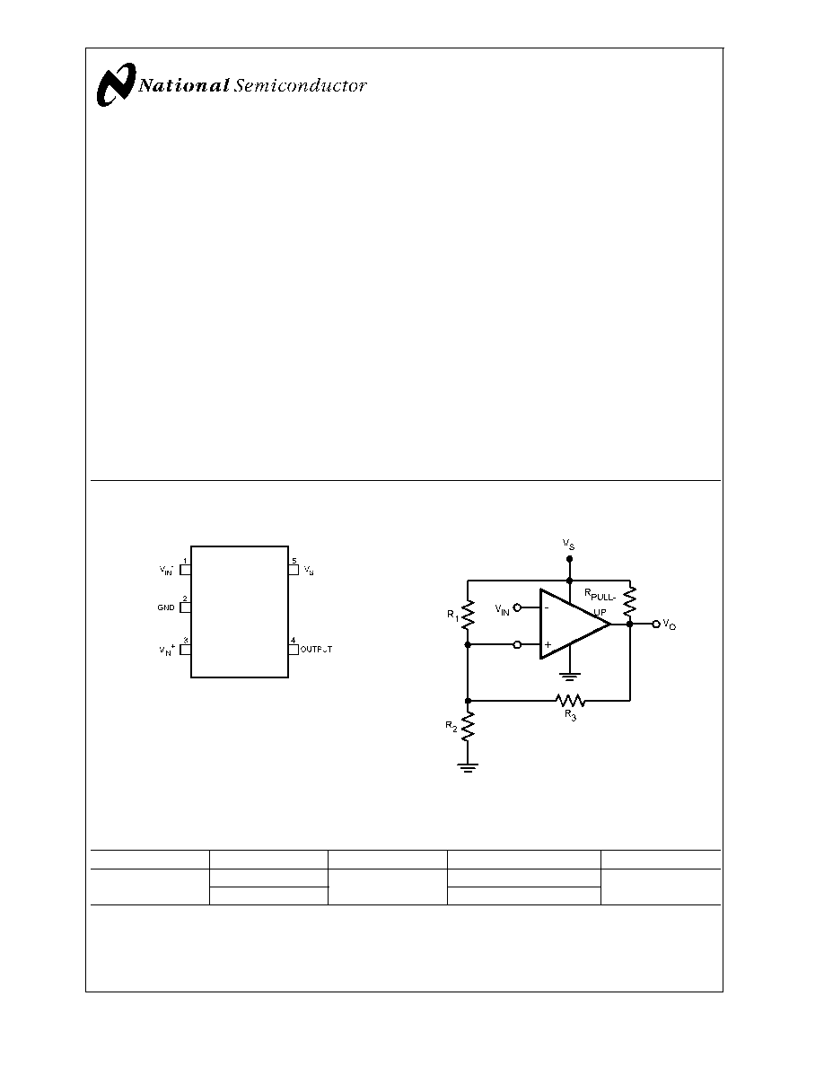
Connection Diagram
SOT23-5
20022108
Top View
Typical Circuit
Ordering Information
Package
Part Number
Package Marking
Transport Media
NSC Drawing
5-Pin SOT-23
LM397MF
C397
1k Units Tape and Reel
MF05A
LM397MFX
3k Units Tape and Reel
20022109
FIGURE 1. Inverting Comparator with Hysteresis
June 2001
LM397
Single
General
Purpose
V
oltage
Comparator
© 2001 National Semiconductor Corporation
DS200221
www.national.com
Absolute Maximum Ratings
(Note 1)
If Military/Aerospace specified devices are required,
please contact the National Semiconductor Sales Office/
Distributors for availability and specifications.
ESD Tolerance
Human Body Model
2KV (Note 2)
Machine Model
200V (Note 3)
V
IN
Differential
30V
Supply Voltages
30V or
±
15V
Voltage at Input Pins
-0.3V to 30V
Storage Temperature Range
-65∞C to +150∞C
Junction Temperature (Note 4)
+150∞C
Soldering Information
Infrared or Convection (20 sec.)
235∞C
Wave Soldering (10 sec.)
260∞C
Operating Ratings
(Note 1)
Supply Voltage, V
S
5V to 30V
Junction Temperature Range (Note 4)
-40∞C to +85∞C
Package Thermal Resistance (Note 4)
SOT23-5
168∞C/W
Electrical Characteristics
Unless otherwise specified, all limits guaranteed for at T
J
= 25∞C, V
S
= 5V. Bold-
face limits apply at temperature extremes.
Symbol
Parameter
Conditions
Min
(Note 6)
Typ
(Note 5)
Max
(Note 6)
Units
V
OS
Input Offset Voltage
V
S
= 5V to 30V,
V
O
= 1.4V, V
CM
= 0V
2
7
10
mV
I
OS
Input Offset Current
V
O
= 1.4V, V
CM
= 0V
1.6
50
250
nA
I
B
Input Bias Current
V
O
= 1.4V, V
CM
= 0V
10
250
400
nA
I
S
Supply Current
R
L
= Open, V
S
= 5V
0.25
0.7
mA
R
L
= Open, V
S
= 30V
0.30
2
I
O
Output Sink Current
V
IN+
= 1V,V
IN-
= 0V, V
O
= 1.5V
6
13
mA
I
LEAKAGE
Output Leakage Current
V
IN+
= 1V,V
IN-
= 0V, V
O
= 5V
0.1
nA
V
IN+
= 1V,V
IN-
= 0V, V
O
= 30V
1
µA
V
OL
Output Voltage Low
I
O
= -4mA, V
IN+
= 0V,V
IN-
= 1V
180
400
700
mV
V
CM
Common-Mode Input Voltage
Range
V
S
= 5V to 30V (Note 7)
V
S
- 1.5V
0
V
V
S
- 2V
0
LM397
www.national.com
2
Electrical Characteristics
Unless otherwise specified, all limits guaranteed for at T
J
= 25∞C, V
S
= 5V.
Boldface limits apply at temperature extremes. (Continued)
Symbol
Parameter
Conditions
Min
(Note 6)
Typ
(Note 5)
Max
(Note 6)
Units
A
V
Voltage Gain
V
S
= 15V, V
O
= 1.4V to 11.4V,
R
L
>
= 15k
connected to V
S
120
V/mV
t
PHL
Propagation Delay (High to Low)
Input Overdrive = 5mV
R
L
= 5.1k
connected to 5V,
C
L
= 15pF
900
ns
Input Overdrive = 50mV
R
L
= 5.1k
connected to 5V,
C
L
= 15pF
250
t
PLH
Propagation Delay (Low to High)
Input Overdrive = 5mV
R
L
= 5.1k
connected to 5V,
C
L
= 15pF
940
µs
Input Overdrive = 50mV
R
L
= 5.1k
connected to 5V,
C
L
= 15pF
440
ns
Note 1: Absolute Maximum Ratings indicate limits beyond which damage to the device may occur. Operating Ratings indicate conditions for which the device is
intended to be functional, but specific performance is not guaranteed. For guaranteed specifications and the test conditions, see the Electrical Characteristics.
Note 2: Human body model, 1.5k
in series with 100pF.
Note 3: Machine model, 0
in series with 200pF.
Note 4: The maximum power dissipation is a function of T
J(MAX)
,
JA
, and T
A
. The maximum allowable power dissipation at any ambient temperature is
P
D
= (T
J(MAX)
- T
A
)/
JA
. All numbers apply for packages soldered directly onto a PC board.
Note 5: Typical values represent the most likely parametric norm.
Note 6: All limits are guaranteed by testing or statistical analysis.
Note 7: The input common-mode voltage of either input should not be permitted to go below the negative rail by more than 0.3V. The upper end of the
common-mode voltage range is V
S
- 1.5V at 25∞C.
LM397
www.national.com
3
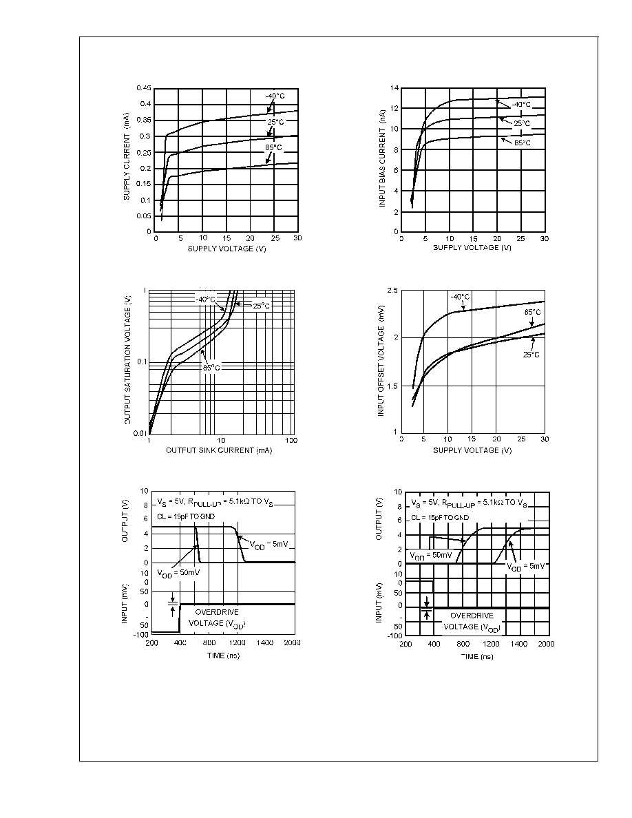
Typical Performance Characteristics
T
A
= 25∞C. Unless otherwise specified.
Supply Current vs. Supply Voltage
Input Bias Current vs. Supply Current
20022103
20022101
Output Saturation Voltage vs. Output Sink Current
Input Offset Voltage vs. Supply Voltage
20022104
20022102
Response Time for Various Input Overdrives ≠ t
PHL
Response Time for Various Input Overdrives ≠ t
PLH
20022105
20022106
LM397
www.national.com
4
Application Notes
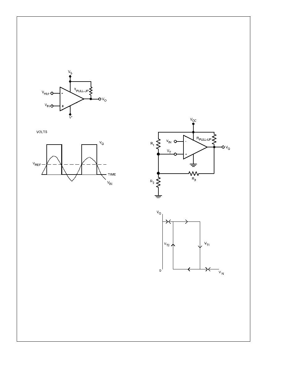
Basic Comparators
A comparator is quite often used to convert an analog signal
to a digital signal. The comparator compares an input volt-
age (V
IN
) at the non-inverting pin to the reference voltage
(V
REF
) at the inverting pin. If V
IN
is less than V
REF
the output
(V
O
) is low (V
OL
). However, if V
IN
is greater than V
REF
, the
output voltage (V
O
) is high (V
OH
). Refer to
Figure 2.
Hysteresis
The basic comparator configuration may oscillate or produce
a noisy output if the applied differential input is near the
comparator's input offset voltage. This tends to occur when
the voltage on the input is equal or very close to the other
input voltage. Adding hysteresis can prevent this problem.
Hysteresis creates two switching thresholds (one for the
rising input voltage and the other for the falling input volt-
age). Hysteresis is the voltage difference between the two
switching thresholds. When both inputs are nearly equal,
hysteresis causes one input to effectively move quickly pass
the other. Thus, effectively moving the input out of region that
oscillation may occur.
For an inverting configured comparator, hysteresis can be
added with a three resistor network and positive feedback.
When input voltage (V
IN
) at the inverting node is less than
non-inverting node (V
T
), the output is high. The equivalent
circuit for the three resistor network is R
1
in parallel with R
3
and in series with R
2
. The lower threshold voltage V
T1
is
calculated by:
V
T1
= ((V
S
R
2
) / (((R
1
R
3
) / (R
1
+ R
3
)) + R
2
))
When V
IN
is greater than V
T
, the output voltage is low. The
equivalent circuit for the three resistor network is R
2
in
parallel with R
3
and in series with R
1
. The upper threshold
voltage V
T2
is calculated by:
V
T2
= V
S
((R
2
R
3
) / (R
2
+ R
3
)) / (R
1
+ ((R
2
R
3
) / (R
2
+
R
3
)))
The hysteresis is defined as
V
IN
= V
T1
≠ V
T2
20022110
20022111
FIGURE 2. Basic Comparator
20022112
20022113
FIGURE 3. Inverting Configured Comparator ≠ LM397
LM397
www.national.com
5