
TL F 5957
CD4024BMCD4024BC
7-Stage
Ripple
Carry
Binary
Counter
March 1988
CD4024BM CD4024BC
7-Stage Ripple Carry Binary Counter
General Description
The CD4024BM CD4024BC is a 7-stage ripple-carry binary
counter
Buffered outputs are externally available from
stages 1 through 7 The counter is reset to its logical ``0''
stage by a logical ``1'' on the reset input The counter is
advanced one count on the negative transition of each
clock pulse
Features
Y
Wide supply voltage range
3 0V to 15V
Y
High noise immunity
0 45 V
DD
(typ )
Y
Low power TTL
Fan out of 2 driving 74L
compatibility
or 1 driving 74LS
Y
High speed
12 MHz (typ )
input pulse rate V
DD
b
V
SS
e
10V
Y
Fully static operation
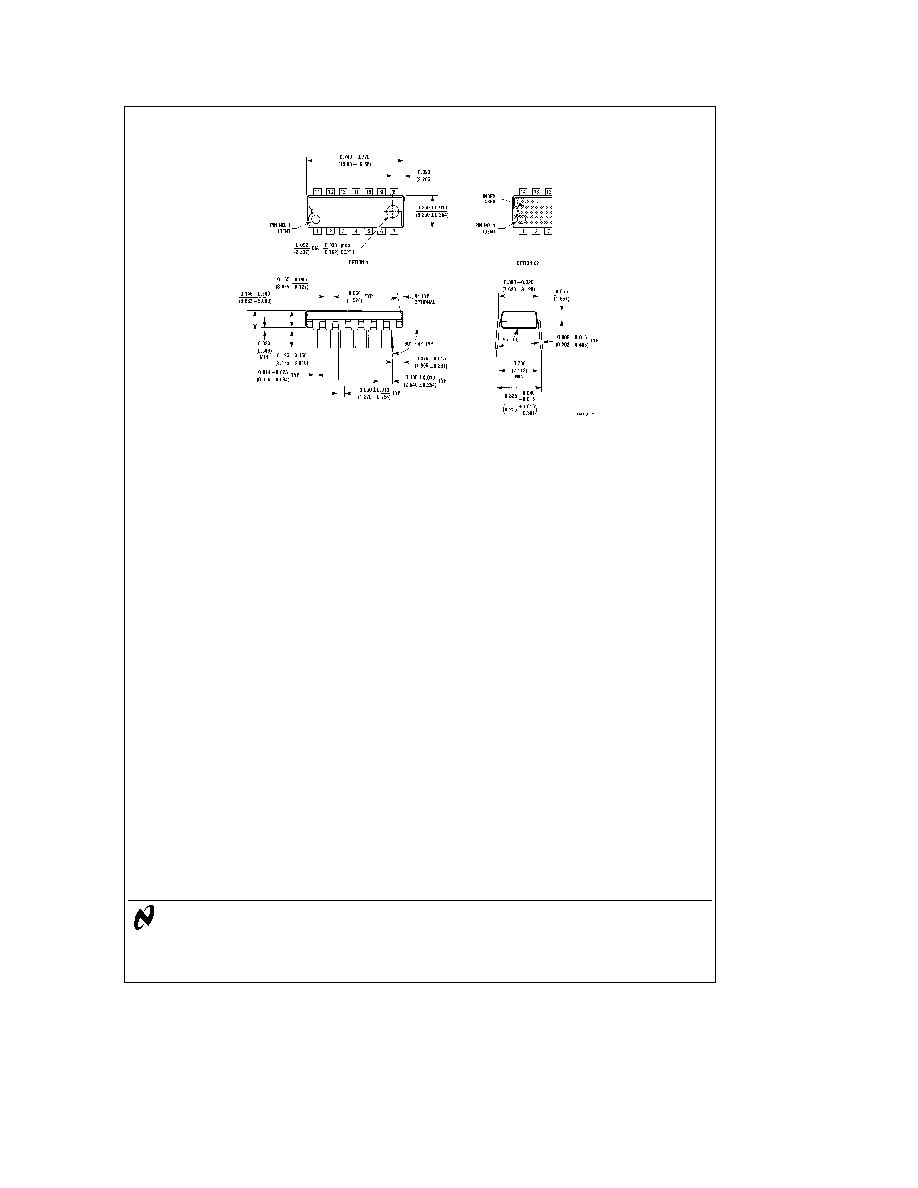
Connection Diagram
Dual-In-Line Package
TL F 5957 � 1
Top View
Order Number CD4024B
Schematic Diagrams
TL F 5957 � 3
Input Logic
Flip-flop logic (1 of 7 identical stages)
TL F 5957 � 4
C1995 National Semiconductor Corporation
RRD-B30M105 Printed in U S A
Absolute Maximum Ratings
(Notes 1
2)
If Military Aerospace specified devices are required
please contact the National Semiconductor Sales
Office Distributors for availability and specifications
DC Supply Voltage (V
DD
)
b
0 5 to
a
18 V
DC
Input Voltage (V
IN
)
b
0 5 to V
DD
a
0 5 V
DC
Storage Temperature Range (T
S
)
b
65 C to
a
150 C
Power Dissipation (P
D
)
Dual-In-Line
700 mW
Small Outline
500 mW
Lead Temp (Soldering 10 sec ) (T
L
)
260 C
Recommended Operating
Conditions
(Note 2)
DC Supply Voltage (V
DD
)
a
3 to
a
15 V
DC
Input Voltage (V
IN
)
0 to V
DD
V
DC
Operating Temperature Range (T
A
)
CD4024BM
b
55 C to
a
125 C
CD4024BC
b
40 C to
a
85 C
DC Electrical Characteristics
CD4024BM (Note 2)
Symbol
Parameter
Conditions
b
55 C
a
25 C
a
125 C
Units
Min
Max
Min
Typ
Max
Min
Max
I
DD
Quiescent Device Current V
DD
e
5V
5
0 3
5
150
m
A
V
DD
e
10V
10
0 5
10
300
m
A
V
DD
e
15V
20
0 7
20
600
m
A
V
OL
Low Level Output Voltage
l
l
O
l
k
1 mA
V
DD
e
5V
0 05
0
0 05
0 05
V
V
DD
e
10V
0 05
0
0 05
0 05
V
V
DD
e
15V
0 05
0
0 05
0 05
V
V
OH
High Level Output Voltage
l
l
O
l
k
1 mA
V
DD
e
5V
4 95
4 95
5
4 95
V
V
DD
e
10V
9 95
9 95
10
9 95
V
V
DD
e
15V
14 95
14 95
15
14 95
V
V
IL
Low Level Input Voltage
l
l
O
l
k
1 mA
V
DD
e
5V V
O
e
0 5V or 4 5V
1 5
2
1 5
1 5
V
V
DD
e
10V V
O
e
1 0V or 9 0V
3 0
4
3 0
3 0
V
V
DD
e
15V V
O
e
1 5V or 13 5V
4 0
6
4 0
4 0
V
V
IH
High Level Input Voltage
l
l
O
l
k
1 mA
V
DD
e
5V V
O
e
0 5V or 4 5V
3 5
3 5
3
3 5
V
V
DD
e
10V V
O
e
1 0V or 9 0V
7 0
7 0
6
7 0
V
V
DD
e
15V V
O
e
1 5V or 13 5V
11 0
11 0
9
11 0
V
I
OL
Low Level Output Current V
DD
e
5V V
O
e
0 4V
0 64
0 51
0 88
0 36
mA
(Note 3)
V
DD
e
10V V
O
e
0 5V
1 6
1 3
2 25
0 9
mA
V
DD
e
15V V
O
e
1 5V
4 2
3 4
8 8
2 4
mA
I
OH
High Level Output Current V
DD
e
5V V
O
e
4 6V
b
0 64
b
0 51
b
0 88
b
0 36
mA
(Note 3)
V
DD
e
10V V
O
e
9 5V
b
1 6
b
1 3
b
2 25
b
0 9
mA
V
DD
e
15V V
O
e
13 5V
b
4 2
b
3 4
b
8 8
b
2 4
mA
I
IN
Input Current
V
DD
e
15V V
IN
e
0V
b
0 10
b
10
b
5
b
0 10
b
1 0
m
A
V
DD
e
15V V
IN
e
15V
0 10
10
b
5
0 10
1 0
m
A
DC Electrical Characteristics
CD4024BC (Note 2)
Symbol
Parameter
Conditions
b
40 C
a
25 C
a
85 C
Units
Min
Max
Min
Typ
Max
Min
Max
I
DD
Quiescent Device Current
V
DD
e
5V
20
0 3
20
150
m
A
V
DD
e
10V
40
0 5
40
300
m
A
V
DD
e
15V
60
0 7
80
600
m
A
V
OL
Low Level Output Voltage
l
l
O
l
k
1 mA
V
DD
e
5V
0 05
0
0 05
0 05
V
V
DD
e
10V
0 05
0
0 05
0 05
V
V
DD
e
15V
0 05
0
0 05
0 05
V
V
OH
High Level Output Voltage
l
l
O
l
k
1 mA
V
DD
e
5V
4 95
4 95
5
4 95
V
V
DD
e
10V
9 95
9 95
10
9 95
V
V
DD
e
15V
14 95
14 95
15
14 95
V
2
DC Electrical Characteristics
CD4024BC (Note 2) (Continued)
Symbol
Parameter
Conditions
b
40 C
a
25 C
a
85 C
Units
Min
Max
Min
Typ
Max
Min
Max
V
IL
Low Level Input Voltage
l
l
O
l
k
1 mA
V
DD
e
5V V
O
e
0 5V or 4 5V
1 5
2
1 5
1 5
V
V
DD
e
10V V
O
e
1 0V or 9 0V
3 0
4
3 0
3 0
V
V
DD
e
15V V
O
e
1 5V or 13 5V
4 0
6
4 0
4 0
V
V
IH
High Level Input Voltage
l
l
O
l
k
1 mA
V
DD
e
5V V
O
e
0 5V or 4 5V
3 5
3 5
3
3 5
V
V
DD
e
10V V
O
e
1 0V or 9 0V
7 0
7 0
6
7 0
V
V
DD
e
15V V
O
e
1 5V or 13 5V
11 0
11 0
9
11 0
V
I
OL
Low Level Output Current V
DD
e
5V V
O
e
0 4V
0 52
0 44
0 88
0 36
mA
(Note 3)
V
DD
e
10V V
O
e
0 5V
1 3
1 1
2 25
0 9
mA
V
DD
e
15V V
O
e
1 5V
3 6
3 0
8 8
2 4
mA
I
OH
High Level Output Current V
DD
e
5V V
O
e
4 6V
b
0 52
b
0 44
b
0 88
b
0 36
mA
(Note 3)
V
DD
e
10V V
O
e
9 5V
b
1 3
b
1 1
b
2 25
b
0 9
mA
V
DD
e
15V V
O
e
13 5V
b
3 6
b
3 0
b
8 8
b
2 4
mA
I
IN
Input Current
V
DD
e
15V V
IN
e
0V
b
0 30
b
10
b
5
b
0 30
b
1 0
m
A
V
DD
e
15V V
IN
e
15V
0 30
10
b
5
0 30
1 0
m
A
AC Electrical Characteristics
T
A
e
25 C C
L
e
50 pF R
L
e
200 k t
r
and t
f
e
20 ns unless otherwise specified
Symbol
Parameter
Conditions
Min
Typ
Max
Units
t
PHL
t
PLH
Propagation Delay Time
V
DD
e
5V
185
350
ns
to Q1 Output
V
DD
e
10V
85
125
ns
V
DD
e
15V
70
100
ns
t
THL
t
TLH
Transition Time
V
DD
e
5V
100
200
ns
V
DD
e
10V
50
100
ns
V
DD
e
15V
40
80
ns
t
WL
t
WH
Minimum Input Pulse Width
V
DD
e
5V
75
200
ns
V
DD
e
10V
40
110
ns
V
DD
e
15V
35
90
ns
t
RCL
t
FCL
Input Rise and Fall Time
V
DD
e
5V
15
m
s
V
DD
e
10V
10
m
s
V
DD
e
15V
8
m
s
f
CL
Maximum Input Pulse Frequency
V
DD
e
5V
1 5
5
MHz
V
DD
e
10V
4
12
MHz
V
DD
e
15V
5
15
MHz
t
PHL
Reset Propagation Delay Time
V
DD
e
5V
185
350
ns
V
DD
e
10V
85
125
ns
V
DD
e
15V
70
100
ns
t
WH
Reset Minimum Pulse Width
V
DD
e
5V
185
350
ns
V
DD
e
10V
85
125
ns
V
DD
e
15V
70
100
ns
C
IN
Input Capacitance (Note 4)
Any Input
5
7 5
pF
AC Parameters are guaranteed by DC correlated testing
Note 1
``Absolute Maximum Ratings'' are those values beyond which the safety of the device cannot be guaranteed they are not meant to imply that the devices
should be operated at these limits The table of ``Recommended Operating Conditions'' and ``Electrical Characteristics'' provides conditions for actual device
operation
Note 2
V
SS
e
0V unless otherwise specified
Note 3
I
OH
and I
OL
are tested one output at a time
Note 4
Capacitance is guaranteed by periodic tesing
3
Logic Diagram
TL F 5957 � 2
4
Physical Dimensions
inches (millimeters)
Ceramic Dual-In-Line Package (J)
Order Number CD4024BMJ or CD402BCJ
NS Package Number J14A
5
CD4024BMCD4024BC
7-Stage
Ripple
Carry
Binary
Counter
Physical Dimensions
inches (millimeters) (Continued)
Molded Dual-In-Line Package (N)
Order Number CD4024BMN or CD402BCN
NS Package Number N14A
LIFE SUPPORT POLICY
NATIONAL'S PRODUCTS ARE NOT AUTHORIZED FOR USE AS CRITICAL COMPONENTS IN LIFE SUPPORT
DEVICES OR SYSTEMS WITHOUT THE EXPRESS WRITTEN APPROVAL OF THE PRESIDENT OF NATIONAL
SEMICONDUCTOR CORPORATION As used herein
1 Life support devices or systems are devices or
2 A critical component is any component of a life
systems which (a) are intended for surgical implant
support device or system whose failure to perform can
into the body or (b) support or sustain life and whose
be reasonably expected to cause the failure of the life
failure to perform when properly used in accordance
support device or system or to affect its safety or
with instructions for use provided in the labeling can
effectiveness
be reasonably expected to result in a significant injury
to the user
National Semiconductor
National Semiconductor
National Semiconductor
National Semiconductor
Corporation
Europe
Hong Kong Ltd
Japan Ltd
1111 West Bardin Road
Fax (a49) 0-180-530 85 86
13th Floor Straight Block
Tel 81-043-299-2309
Arlington TX 76017
Email cnjwge tevm2 nsc com
Ocean Centre 5 Canton Rd
Fax 81-043-299-2408
Tel 1(800) 272-9959
Deutsch Tel (a49) 0-180-530 85 85
Tsimshatsui Kowloon
Fax 1(800) 737-7018
English
Tel (a49) 0-180-532 78 32
Hong Kong
Fran ais Tel (a49) 0-180-532 93 58
Tel (852) 2737-1600
Italiano
Tel (a49) 0-180-534 16 80
Fax (852) 2736-9960
National does not assume any responsibility for use of any circuitry described no circuit patent licenses are implied and National reserves the right at any time without notice to change said circuitry and specifications