TL F 5961
CD4030MCD4030C
Quad
EXCLUSIVE-OR
Gate
February 1988
CD4030M CD4030C Quad EXCLUSIVE-OR Gate
General Description
The EXCLUSIVE-OR gates are monolithic complementary
MOS (CMOS) integrated circuits constructed with N- and P-
channel enhancement mode transistors All inputs are pro-
tected against static discharge with diodes to V
DD
and V
SS
Features
Y
Wide supply voltage range
3 0V to 15V
Y
Low power
100 nW (typ )
Y
Medium speed
t
PHL
e
t
PLH
e
40 ns (typ )
operation
at C
L
e
15 pF 10V supply
Y
High noise immunity
0 45 V
CC
(typ )
Applications
Y
Automotive
Y
Data terminals
Y
Instrumentation
Y
Medical electronics
Y
Industrial controls
Y
Remote metering
Y
Computers
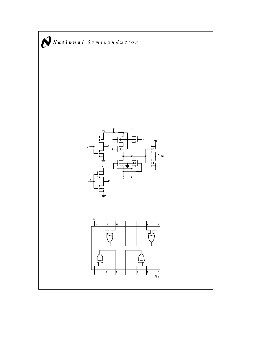
Schematic Diagram
TL F 5961 � 1
Connection Diagram
Dual-In-Line Package
TL F 5961 � 2
Order Number CD4030
C1995 National Semiconductor Corporation
RRD-B30M105 Printed in U S A
Absolute Maximum Ratings
If Military Aerospace specified devices are required
please contact the National Semiconductor Sales
Office Distributors for availability and specifications
Voltage at Any Pin (Note 1)
V
SS
b
0 3V to V
SS
a
15 5V
Operating Temperature Range
CD4030M
b
55 C to
a
125 C
CD4030C
b
40 C to
a
85 C
Storage Temperature Range
b
65 C to
a
150 C
Power Dissipation (P
D
)
Dual-In-Line
700 mW
Small Outline
500 mW
Operating V
DD
Range
V
SS
a
3 0V to V
SS
a
15V
Lead Temperature
(Soldering 10 seconds)
260 C
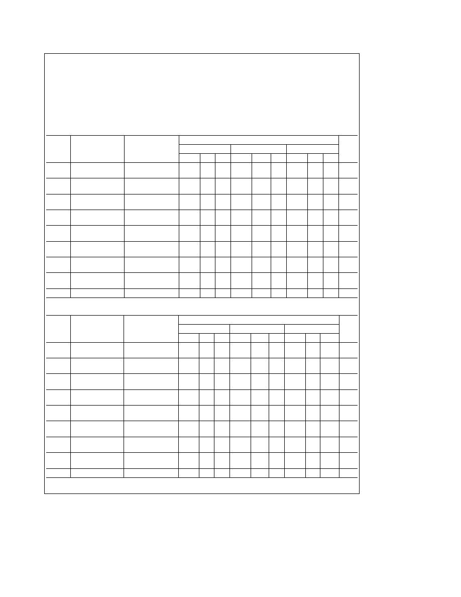
DC Electrical Characteristics
CD4030M
Limits
Symbol
Parameter
Conditions
b
55 C
a
25 C
a
125 C
Units
Min
Typ
Max
Min
Typ
Max
Min
Typ
Max
I
L
Quiescent Device
V
DD
e
5 0V
0 5
0 005
0 5
30
m
A
Current
V
DD
e
10V
1 0
0 01
1 0
60
m
A
P
D
Quiescent Device
V
DD
e
5 0V
2 5
0 025
2 5
150
m
W
Dissipation Package
V
DD
e
10V
10
0 1
10
600
m
W
V
OL
Output Voltage
V
DD
e
5 0V
0 05
0
0 05
0 05
V
Low Level
V
DD
e
10V
0 05
0
0 05
0 05
V
V
OH
Output Voltage
V
DD
e
5 0V
4 95
4 95
5 0
4 95
V
High Level
V
DD
e
10V
9 95
9 95
10
9 95
V
V
NL
Noise Immunity
V
DD
e
5 0V
1 5
1 5
2 25
1 4
V
(All Inputs)
V
DD
e
10V
3 0
3 0
4 5
2 9
V
V
NH
Noise Immunity
V
DD
e
5 0V
1 4
1 5
2 25
1 5
V
(All Inputs)
V
DD
e
10V
2 9
3 0
4 5
3 0
V
I
D
N
Output Drive Current
V
DD
e
5 0V
0 75
0 6
1 2
0 45
mA
N-Channel (Note 2)
V
DD
e
10V
1 5
1 2
2 4
0 9
mA
I
D
P
Output Drive Current
V
DD
e
5 0V
b
0 45
b
0 3
b
0 6
b
0 21
mA
P-Channel (Note 2)
V
DD
e
10V
b
0 95
b
0 65
b
1 3
b
0 45
mA
I
I
Input Current
V
I
e
0V or V
I
e
V
DD
10
pA
DC Electrical Characteristics
CD4030C
Limits
Symbol
Parameter
Conditions
b
40 C
a
25 C
a
85 C
Units
Min
Typ
Max
Min
Typ
Max
Min
Typ
Max
I
L
Quiescent Device
V
DD
e
5 0V
5 0
0 05
5 0
70
m
A
Current
V
DD
e
10V
10
0 1
10
140
m
A
P
D
Quiescent Device
V
DD
e
5 0V
25
0 25
25
350
m
W
Dissipation Package
V
DD
e
10V
100
1 0
100
1 400
m
W
V
OL
Output Voltage
V
DD
e
5 0V
0 05
0
0 05
0 05
V
Low Level
V
DD
e
10V
0 05
0
0 05
0 05
V
V
OH
Output Voltage
V
DD
e
5 0V
4 95
4 95
5 0
4 95
V
High Level
V
DD
e
10V
9 95
9 95
10
9 95
V
V
NL
Noise Immunity
V
DD
e
5 0V
1 5
1 5
2 25
1 4
V
(All Inputs)
V
DD
e
10V
3 0
3 0
4 5
2 9
V
V
NH
Noise Immunity
V
DD
e
5 0V
1 4
1 5
2 25
1 5
V
(All Inputs)
V
DD
e
10V
2 9
3 0
4 5
3 0
V
I
D
N
Output Drive Current
V
DD
e
5 0V
0 35
0 3
1 2
0 25
mA
N-Channel (Note 2)
V
DD
e
10V
0 7
0 6
2 4
0 5
mA
I
D
P
Output Drive Current
V
DD
e
5 0V
b
0 21
b
0 15
b
0 6
b
0 12
mA
P-Channel (Note 2)
V
DD
e
10 V
b
0 45
b
0 32
b
1 3
b
0 25
mA
I
I
Input Current
V
I
e
0V or V
I
e
V
DD
10
pA
2
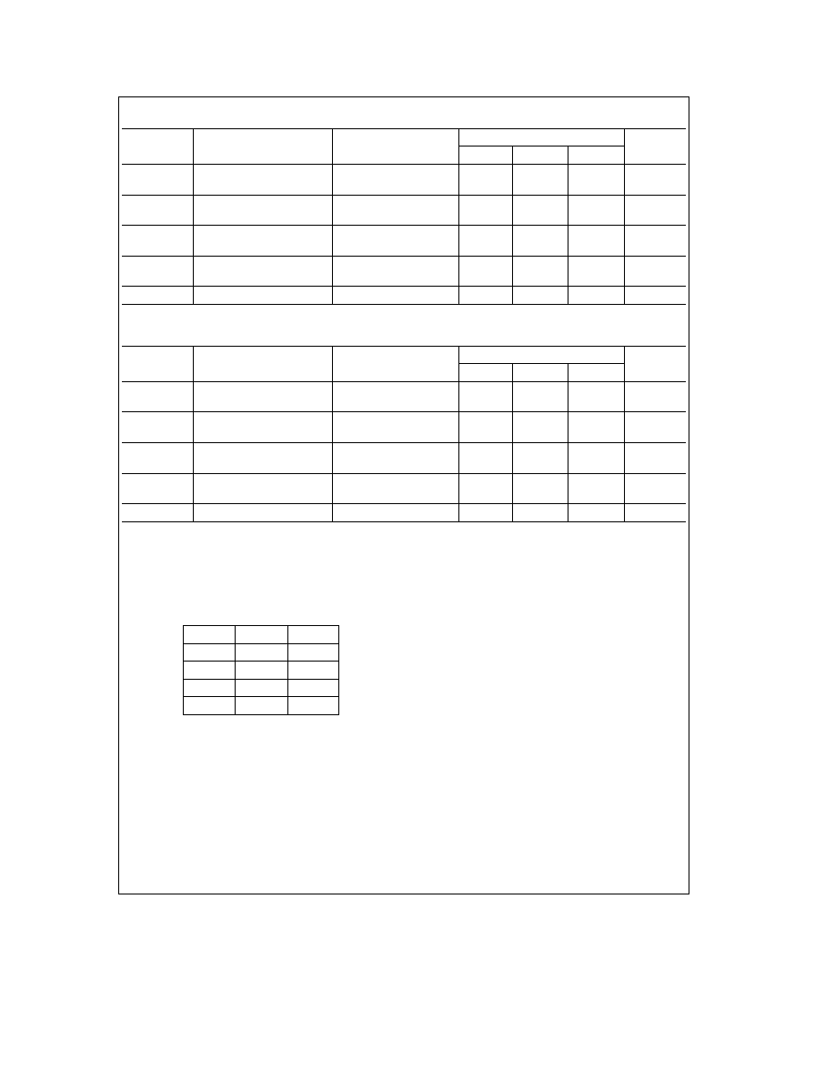
AC Electrical Characteristics
CD4030M
Symbol
Parameter
Conditions
Limits
Units
Min
Typ
Max
t
PHL
Propagation Delay Time
V
DD
e
5 0V
100
200
ns
V
DD
e
10V
40
100
ns
t
PLH
Propagation Delay Time
V
DD
e
5 0V
100
200
ns
V
DD
e
10V
40
100
ns
t
THL
Transition Time
V
DD
e
5 0V
70
150
ns
High to Low Level
V
DD
e
10V
25
75
ns
t
TLH
Transition Time
V
DD
e
5 0V
80
150
ns
Low to High Level
V
DD
e
10V
30
75
ns
C
I
Input Capacitance
V
I
e
0V or V
I
e
V
DD
5 0
pF
AC Parameters are guaranteed by DC correlated testing
AC Electrical Characteristics
CD4030C
Symbol
Parameter
Conditions
Limits
Units
Min
Typ
Max
t
PHL
Propagation Delay Time
V
DD
e
5 0V
100
300
ns
V
DD
e
10V
40
150
ns
t
PLH
Propagation Delay Time
V
DD
e
5 0V
100
300
ns
V
DD
e
10V
40
150
ns
t
THL
Transition Time
V
DD
e
5 0V
70
300
ns
High to Low Level
V
DD
e
10V
25
150
ns
t
TLH
Transition Time
V
DD
e
5 0V
80
300
ns
Low to High Level
V
DD
e
10V
30
150
ns
C
I
Input Capacitance
V
I
e
0V or V
I
e
V
DD
5 0
pF
AC Parameters are guaranteed by DC correlated testing
Note 1
This device should not be connected to circuits with power on because high transient voltages may cause permanent damage
Note 2
I
D
N and I
D
P are tested one output at a time
Truth Table
(For One of Four Identical Gates)
A
B
J
0
0
0
1
0
1
0
1
1
1
1
0
Where ``1''
e
High Level
``0''
e
Low Level
3
CD4030MCD4030C
Quad
EXCLUSIVE-OR
Gate
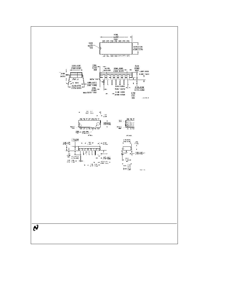
Physical Dimensions
inches (millimeters)
Ceramic Dual-In-Line Package (J)
Order Number CD4030MJ or CD4030CJ
NS Package Number J14A
Molded Dual-In-Line Package (N)
Order Number CD4030MN or CD4030CN
NS Package Number N14A
LIFE SUPPORT POLICY
NATIONAL'S PRODUCTS ARE NOT AUTHORIZED FOR USE AS CRITICAL COMPONENTS IN LIFE SUPPORT
DEVICES OR SYSTEMS WITHOUT THE EXPRESS WRITTEN APPROVAL OF THE PRESIDENT OF NATIONAL
SEMICONDUCTOR CORPORATION As used herein
1 Life support devices or systems are devices or
2 A critical component is any component of a life
systems which (a) are intended for surgical implant
support device or system whose failure to perform can
into the body or (b) support or sustain life and whose
be reasonably expected to cause the failure of the life
failure to perform when properly used in accordance
support device or system or to affect its safety or
with instructions for use provided in the labeling can
effectiveness
be reasonably expected to result in a significant injury
to the user
National Semiconductor
National Semiconductor
National Semiconductor
National Semiconductor
Corporation
Europe
Hong Kong Ltd
Japan Ltd
1111 West Bardin Road
Fax (a49) 0-180-530 85 86
13th Floor Straight Block
Tel 81-043-299-2309
Arlington TX 76017
Email cnjwge tevm2 nsc com
Ocean Centre 5 Canton Rd
Fax 81-043-299-2408
Tel 1(800) 272-9959
Deutsch Tel (a49) 0-180-530 85 85
Tsimshatsui Kowloon
Fax 1(800) 737-7018
English
Tel (a49) 0-180-532 78 32
Hong Kong
Fran ais Tel (a49) 0-180-532 93 58
Tel (852) 2737-1600
Italiano
Tel (a49) 0-180-534 16 80
Fax (852) 2736-9960
National does not assume any responsibility for use of any circuitry described no circuit patent licenses are implied and National reserves the right at any time without notice to change said circuitry and specifications