TL F 5662
CD4051BMCD4051BC
CD4052BMCD4052BC
CD4053BMCD4053BC
Analog
MultiplexerDemultiplexers
October 1989
CD4051BM CD4051BC Single 8-Channel Analog
Multiplexer Demultiplexer
CD4052BM CD4052BC Dual 4-Channel Analog
Multiplexer Demultiplexer
CD4053BM CD4053BC Triple 2-Channel Analog
Multiplexer Demultiplexer
General Description
These analog multiplexers demultiplexers are digitally con-
trolled analog switches having low ``ON'' impedance and
very low ``OFF'' leakage currents Control of analog signals
up to 15V
p-p
can be achieved by digital signal amplitudes of
3 ≠ 15V For example if V
DD
e
5V V
SS
e
0V and V
EE
e b
5V
analog signals from
b
5V to
a
5V can be controlled by digi-
tal inputs of 0 ≠ 5V The multiplexer circuits dissipate ex-
tremely low quiescent power over the full V
DD
b
V
SS
and
V
DD
b
V
EE
supply voltage ranges independent of the logic
state of the control signals When a logical ``1'' is present at
the inhibit input terminal all channels are ``OFF''
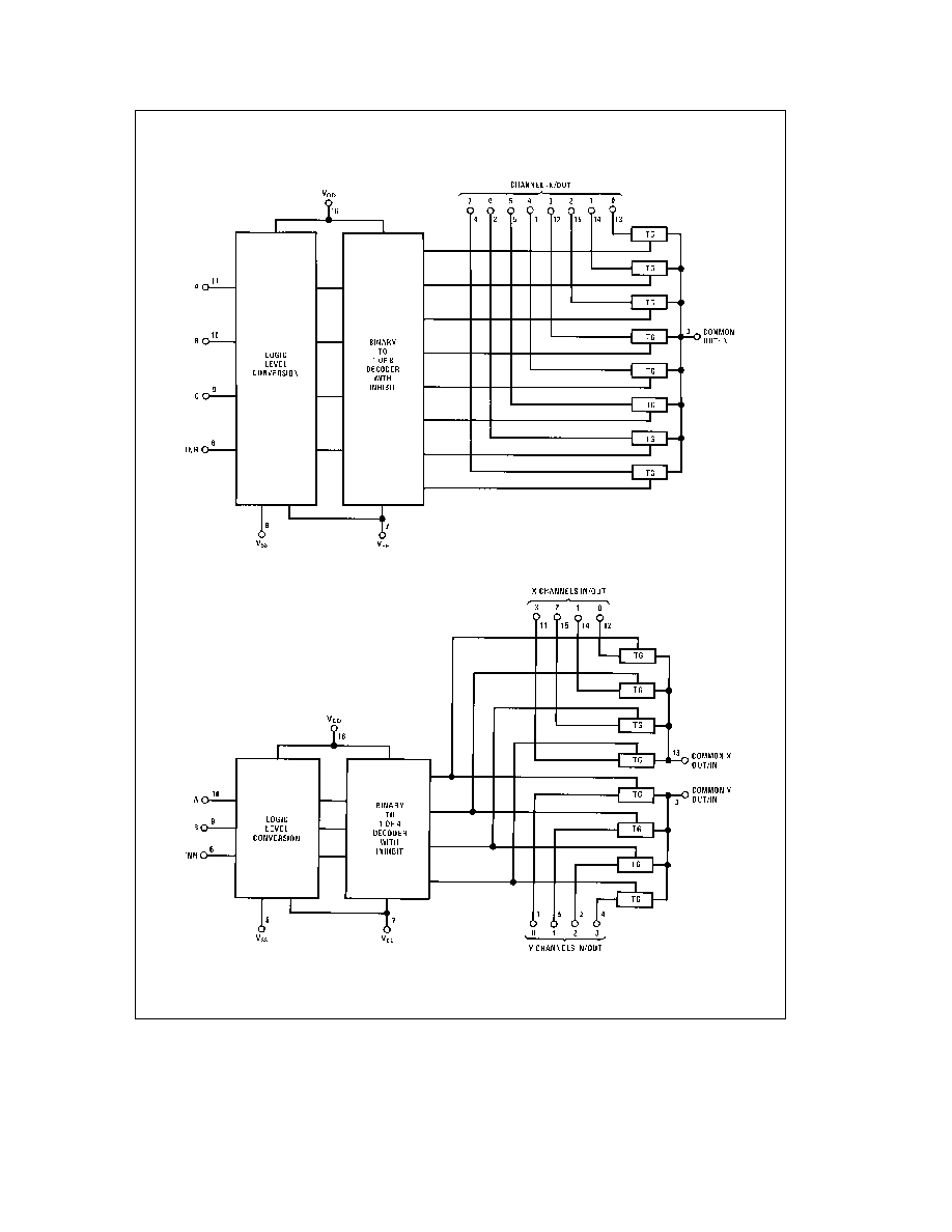
CD4051BM CD4051BC is a single 8-channel multiplexer
having three binary control inputs A B and C and an inhibit
input The three binary signals select 1 of 8 channels to be
turned ``ON'' and connect the input to the output
CD4052BM CD4052BC is a differential 4-channel multiplex-
er having two binary control inputs A and B and an inhibit
input The two binary input signals select 1 or 4 pairs of
channels to be turned on and connect the differential ana-
log inputs to the differential outputs
CD4053BM CD4053BC is a triple 2-channel multiplexer
having three separate digital control inputs A B and C and
an inhibit input Each control input selects one of a pair of
channels which are connected in a single-pole double-throw
configuration
Features
Y
Wide range of digital and analog signal levels digital
3 ≠ 15V analog to 15V
p-p
Y
Low ``ON'' resistance 80X (typ ) over entire 15V
p-p
sig-
nal-input range for V
DD
b
V
EE
e
15V
Y
High ``OFF'' resistance channel leakage of
g
10 pA
(typ ) at V
DD
b
V
EE
e
10V
Y
Logic level conversion for digital addressing signals of
3 ≠ 15V (V
DD
b
V
SS
e
3 ≠ 15V) to switch analog signals to
15 V
p-p
(V
DD
b
V
EE
e
15V)
Y
Matched switch characteristics
D
R
ON
e
5X (typ ) for
V
DD
b
V
EE
e
15V
Y
Very low quiescent power dissipation under all digital-
control input and supply conditions
1 mW (typ ) at
V
DD
b
V
SS
e
V
DD
b
V
EE
e
10V
Y
Binary address decoding on chip
Connection Diagrams
Dual-In-Line Packages
CD4051BM CD4051BC
CD4052BM CD4052BC
CD4053BM CD4053BC
TL F 5662 ≠ 1
Order Number CD4051B CD4052B or CD4053B
C1995 National Semiconductor Corporation
RRD-B30M105 Printed in U S A

Absolute Maximum Ratings
If Military Aerospace specified devices are required
please contact the National Semiconductor Sales
Office Distributors for availability and specifications
DC Supply Voltage (V
DD
)
b
0 5 V
DC
to
a
18 V
DC
Input Voltage (V
IN
)
b
0 5 V
DC
to V
DD
a
0 5 V
DC
Storage Temperature Range (T
S
)
b
65 C to
a
150 C
Power Dissipation (P
D
)
Dual-In-Line
700 mW
Small Outline
500 mW
Lead Temp (T
L
) (soldering 10 sec )
260 C
Recommended Operating
Conditions
DC Supply Voltage (V
DD
)
a
5 V
DC
to
a
15 V
DC
Input Voltage (V
IN
)
0V to V
DD
V
DC
Operating Temperature Range (T
A
)
4051BM 4052BM 4053BM
b
55 C to
a
125 C
4051BC 4052BC 4053BC
b
40 C to
a
85 C
DC Electrical Characteristics
(Note 2)
Symbol
Parameter
Conditions
b
55 C
a
25
a
125 C
Units
Min
Max
Min
Typ
Max
Min
Max
I
DD
Quiescent Device Current
V
DD
e
5V
5
5
150
m
A
V
DD
e
10V
10
10
300
m
A
V
DD
e
15V
20
20
600
m
A
Signal Inputs (V
IS
) and Outputs (V
OS
)
R
ON
``ON'' Resistance (Peak
R
L
e
10 kX
V
DD
e
2 5V
for V
EE
s
V
IS
s
V
DD
)
(any channel
V
EE
e b
2 5V
800
270
1050
1300
X
selected)
or V
DD
e
5V
V
EE
e
0V
V
DD
e
5V
V
EE
e b
5V
310
120
400
550
X
or V
DD
e
10V
V
EE
e
0V
V
DD
e
7 5V
V
EE
e b
7 5V
200
80
240
320
X
or V
DD
e
15V
V
EE
e
0V
D
R
ON
D
``ON'' Resistance
R
L
e
10 kX
V
DD
e
2 5V
Between Any Two
(any channel
V
EE
e b
2 5V
10
X
Channels
selected)
or V
DD
e
5V
V
EE
e
0V
V
DD
e
5V
V
EE
e b
5V
10
X
or V
DD
e
10V
V
EE
e
0V
V
DD
e
7 5V
V
EE
e b
7 5V
5
X
or V
DD
e
15V
V
EE
e
0V
``OFF'' Channel Leakage
V
DD
e
7 5V
V
EE
e b
7 5V
Current any channel
O I
e
g
7 5V I O
e
0V
g
50
g
0 01
g
50
g
500
nA
``OFF''
``OFF'' Channel Leakage
Inhibit
e
7 5V
CD4051
g
200
g
0 08
g
200
g
2000
nA
Current all channels
V
DD
e
7 5V
``OFF'' (Common
V
EE
e b
7 5V
CD4052
g
200
g
0 04
g
200
g
2000
nA
OUT IN)
O I
e
0V
I O
e
g
7 5V
CD4053
g
200
g
0 02
g
200
g
2000
nA
Control Inputs A B C and Inhibit
V
IL
Low Level Input Voltage
V
EE
e
V
SS
R
L
e
1 kX to V
SS
I
IS
k
2 mA on all OFF channels
V
IS
e
V
DD
thru 1 kX
V
DD
e
5V
1 5
1 5
1 5
V
V
DD
e
10V
3 0
3 0
3 0
V
V
DD
e
15V
4 0
4 0
4 0
V
V
IH
High Level Input Voltage
V
DD
e
5
3 5
3 5
3 5
V
V
DD
e
10
7
7
7
V
V
DD
e
15
11
11
11
V
Note 1
``Absolute Maximum Ratings'' are those values beyond which the safety of the device cannot be guaranteed Except for ``Operating Temperature Range''
they are not meant to imply that the devices should be operated at these limits The table of ``Electrical Characteristics'' provides conditions for actual device
operation
Note 2
All voltages measured with respect to V
SS
unless otherwise specified
2

DC Electrical Characteristics
(Note 2) (Continued)
Symbol
Parameter
Conditions
b
40 C
a
25 C
a
85 C
Units
Min
Max
Min
Typ
Max
Min
Max
I
IN
Input Current
V
DD
e
15V
V
EE
e
0V
b
0 1
b
10
b
5
b
0 1
b
1 0
m
A
V
IN
e
0V
V
DD
e
15V
V
EE
e
0V
0 1
10
b
5
0 1
1 0
m
A
V
IN
e
15V
I
DD
Quiescent Device Current
V
DD
e
5V
20
20
150
m
A
V
DD
e
10V
40
40
300
m
A
V
DD
e
15V
80
80
600
m
A
Signal Inputs (V
IS
) and Outputs (V
OS
)
R
ON
``ON'' Resistance (Peak
R
L
e
10 kX
V
DD
e
2 5V
for V
EE
s
V
IS
s
V
DD
)
(any channel
V
EE
e b
2 5V
850
270
1050
1200
X
selected)
or V
DD
e
5V
V
EE
e
0V
V
DD
e
5V
V
EE
e b
5V
330
120
400
520
X
or V
DD
e
10V
V
EE
e
0V
V
DD
e
7 5V
V
EE
e b
7 5V
210
80
240
300
X
or V
DD
e
15V
V
EE
e
0V
D
R
ON
D
``ON'' Resistance
R
L
e
10 kX
V
DD
e
2 5V
Between Any Two
(any channel
V
EE
e b
2 5V
10
X
Channels
selected)
or V
DD
e
5V
V
EE
e
0V
V
DD
e
5V
V
EE
e b
5V
10
X
or V
DD
e
10V
V
EE
e
0V
V
DD
e
7 5V
V
EE
e b
7 5V
5
X
or V
DD
e
15V
V
EE
e
0V
``OFF'' Channel Leakage
V
DD
e
7 5V
V
EE
e b
7 5V
Current any channel ``OFF'' O I
e
g
7 5V I O
e
0V
g
50
g
0 01
g
50
g
500
nA
``OFF'' Channel Leakage
Inhibit
e
7 5V
CD4051
g
200
g
0 08
g
200
g
2000
nA
Current all channels
V
DD
e
7 5V
``OFF'' (Common
V
EE
e b
7 5V
CD4052
g
200
g
0 04
g
200
g
2000
nA
OUT IN)
O I
e
0V
I O
e
g
7 5V
CD4053
g
200
g
0 02
g
200
g
2000
nA
Control Inputs A B C and Inhibit
V
IL
Low Level Input Voltage
V
EE
e
V
SS
R
L
e
1 kX to V
SS
I
IS
k
2 mA on all OFF Channels
V
IS
e
V
DD
thru 1 kX
V
DD
e
5V
1 5
1 5
1 5
V
V
DD
e
10V
3 0
3 0
3 0
V
V
DD
e
15V
4 0
4 0
4 0
V
V
IH
High Level Input Voltage
V
DD
e
5
3 5
3 5
3 5
V
V
DD
e
10
7
7
7
V
V
DD
e
15
11
11
11
V
I
IN
Input Current
V
DD
e
15V
V
EE
e
0V
b
0 1
b
10
b
5
b
0 1
b
1 0
m
A
V
IN
e
0V
V
DD
e
15V
V
EE
e
0V
0 1
10
b
5
0 1
1 0
m
A
V
IN
e
15V
Note 1
``Absolute Maximum Ratings'' are those values beyond which the safety of the device cannot be guaranteed Except for ``Operating Temperature Range''
they are not meant to imply that the devices should be operated at these limits The table of ``Electrical Characteristics'' provides conditions for actual device
operation
Note 2
All voltages measured with respect to V
SS
unless otherwise specified
3
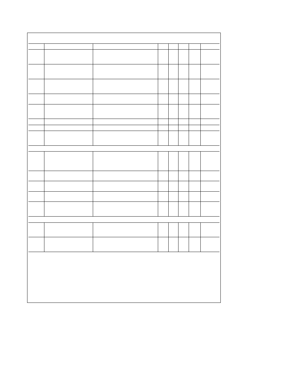
AC Electrical Characteristics
T
A
e
25 C t
r
e
t
f
e
20 ns unless otherwise specified
Symbol
Parameter
Conditions
V
DD
Min
Typ
Max
Units
t
PZH
Propagation Delay Time from
V
EE
e
V
SS
e
0V
5V
600
1200
ns
t
PZL
Inhibit to Signal Output
R
L
e
1 kX
10V
225
450
ns
(channel turning on)
C
L
e
50 pF
15V
160
320
ns
t
PHZ
Propagation Delay Time from
V
EE
e
V
SS
e
0V
5V
210
420
ns
t
PLZ
Inhibit to Signal Output
R
L
e
1 kX
10V
100
200
ns
(channel turning off)
C
L
e
50 pF
15V
75
150
ns
C
IN
Input Capacitance
Control input
5
7 5
pF
Signal Input (IN OUT)
10
15
pF
C
OUT
Output Capacitance
(common OUT IN)
CD4051
10V
30
pF
CD4052
V
EE
e
V
SS
e
0V
10V
15
pF
CD4053
10V
8
pF
C
IOS
Feedthrough Capacitance
0 2
pF
C
PD
Power Dissipation Capacitance
CD4051
110
pF
CD4052
140
pF
CD4053
70
pF
Signal Inputs (V
IS
) and Outputs (V
OS
)
Sine Wave Response
R
L
e
10 kX
(Distortion)
f
IS
e
1 kHz
10V
0 04
%
V
IS
e
5 V
p-p
V
EE
e
V
SI
e
0V
Frequency Response Channel
R
L
e
1 kX V
EE
e
0V V
IS
e
5V
p-p
10V
40
MHz
``ON'' (Sine Wave Input)
20 log
10
V
OS
V
IS
e b
3 dB
Feedthrough Channel ``OFF''
R
L
e
1 kX V
EE
e
V
SS
e
0V V
IS
e
5V
p-p
10V
10
MHz
20 log
10
V
OS
V
IS
e b
40 dB
Crosstalk Between Any Two
R
L
e
1 kX V
EE
e
V
SS
e
0V V
IS
(A)
e
5V
p-p
10V
3
MHz
Channels (frequency at 40 dB)
20 log
10
V
OS
(B) V
IS
(A)
e b
40 dB (Note 3)
t
PHL
Propagation Delay Signal
V
EE
e
V
SS
e
0V
5V
25
55
ns
t
PLH
Input to Signal Output
C
L
e
50 pF
10V
15
35
ns
15V
10
25
ns
Control Inputs A B C and Inhibit
Control Input to Signal
V
EE
e
V
SS
e
0V R
L
e
10 kX at both ends
Crosstalk
of channel
10V
65
mV (peak)
Input Square Wave Amplitude
e
10V
t
PHL
Propagation Delay Time from
V
EE
e
V
SS
e
0V
5V
500
1000
ns
t
PLH
Address to Signal Output
C
L
e
50 pF
10V
180
360
ns
(channels ``ON'' or ``OFF'')
15V
120
240
ns
AC Parameters are guaranteed by DC correlated testing
Note 3
A B are two arbitrary channels with A turned ``ON'' and B ``OFF''
4