 | –≠–ª–µ–∫—Ç—Ä–æ–Ω–Ω—ã–π –∫–æ–º–ø–æ–Ω–µ–Ω—Ç: CD4071BM | –°–∫–∞—á–∞—Ç—å:  PDF PDF  ZIP ZIP |
TL F 5977
CD4071BMCD4071BC
Quad
2-Input
OR
Buffered
B
Series
Gate
CD4081BMCD4081BC
Quad
2-Input
AND
Buffered
B
Series
Gate
February 1988
CD4071BM CD4071BC
Quad 2-Input OR Buffered B Series Gate
CD4081BM CD4081BC
Quad 2-Input AND Buffered B Series Gate
General Description
These quad gates are monolithic complementary MOS
(CMOS) integrated circuits constructed with N- and P-chan-
nel enhancement mode transistors They have equal source
and sink current capabilities and conform to standard B se-
ries output drive The devices also have buffered outputs
which improve transfer characteristics by providing very
high gain
All inputs protected against static discharge with diodes to
V
DD
and V
SS
Features
Y
Low power TTL
Fan out of 2 driving 74L
compatibility
or 1 driving 74LS
Y
5V ≠ 10V ≠ 15V parametric ratings
Y
Symmetrical output characteristics
Y
Maximum input leakage 1 mA at 15V over full tempera-
ture range
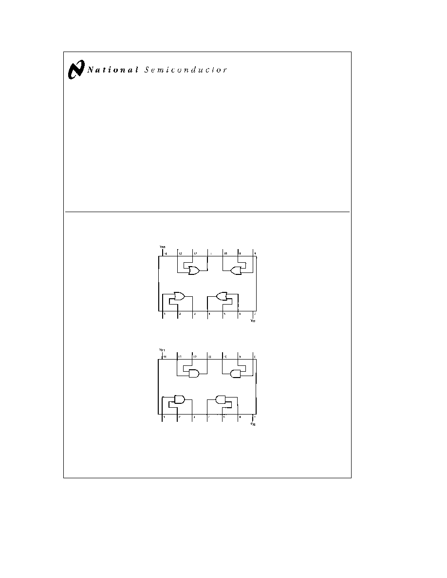
Connection Diagrams
CD4071B Dual-In-Line Package
TL F 5977 ≠ 3
Top View
CD4081B Dual-In-Line Package
TL F 5977 ≠ 6
Top View
Order Number CD4071B or CD4081B
C1995 National Semiconductor Corporation
RRD-B30M105 Printed in U S A
Absolute Maximum Ratings
(Notes 1
2)
If Military Aerospace specified devices are required
please contact the National Semiconductor Sales
Office Distributors for availability and specifications
Voltage at Any Pin
b
0 5V to V
DD
a
0 5V
Power Dissipation (P
D
)
Dual-In-Line
700 mW
Small Outline
500 mW
V
DD
Range
b
0 5 V
DC
to
a
18 V
DC
Storage Temperature (T
S
)
b
65 C to
a
150 C
Lead Temperature (T
L
)
(Soldering 10 seconds)
260 C
Operating Conditions
Operating Range (V
DD
)
3 V
DC
to 15 V
DC
Operating Temperature Range (T
A
)
CD4071BM CD4081BM
b
55 C to
a
125 C
CD4071BC CD4081BC
b
40 C to
a
85 C
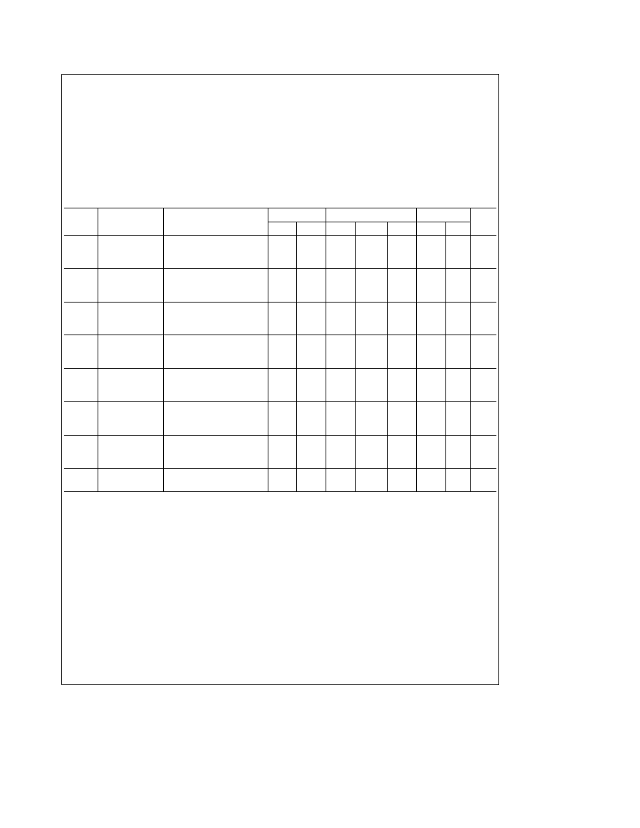
DC Electrical Characteristics
CD4071BM CD4081BM (Note 2)
Symbol
Parameter
Conditions
b
55 C
a
25 C
a
125 C
Units
Min
Max
Min
Typ
Max
Min
Max
I
DD
Quiescent Device
V
DD
e
5V
0 25
0 004
0 25
7 5
m
A
Current
V
DD
e
10V
0 50
0 005
0 50
15
m
A
V
DD
e
15V
1 0
0 006
1 0
30
m
A
V
OL
Low Level
V
DD
e
5V
0 05
0
0 05
0 05
V
Output Voltage
V
DD
e
10V
l
I
O
l
k
1 mA
0 05
0
0 05
0 05
V
V
DD
e
15V
(
0 05
0
0 05
0 05
V
V
OH
High Level
V
DD
e
5V
4 95
4 95
5
4 95
V
Output Voltage
V
DD
e
10V
l
I
O
l
k
1 mA
9 95
9 95
10
9 95
V
V
DD
e
15V
(
14 95
14 95
15
14 95
V
V
IL
Low Level
V
DD
e
5V V
O
e
0 5V
1 5
2
1 5
1 5
V
Input Voltage
V
DD
e
10V V
O
e
1 0V
3 0
4
3 0
3 0
V
V
DD
e
15V V
O
e
1 5V
4 0
6
4 0
4 0
V
V
IH
High Level
V
DD
e
5V V
O
e
4 5V
3 5
3 5
3
3 5
V
Input Voltage
V
DD
e
10V V
O
e
9 0V
7 0
7 0
6
7 0
V
V
DD
e
15V V
O
e
13 5V
11 0
11 0
9
11 0
V
I
OL
Low Level Output
V
DD
e
5V V
O
e
0 4V
0 64
0 51
0 88
0 36
mA
Current
V
DD
e
10V V
O
e
0 5V
1 6
1 3
2 25
0 9
mA
(Note 3)
V
DD
e
15V V
O
e
1 5V
4 2
3 4
8 8
2 4
mA
I
OH
High Level Output
V
DD
e
5V V
O
e
4 6V
b
0 64
b
0 51
b
0 88
b
0 36
mA
Current
V
DD
e
10V V
O
e
9 5V
b
1 6
b
1 3
b
2 25
b
0 9
mA
(Note 3)
V
DD
e
15V V
O
e
13 5V
b
4 2
b
3 4
b
8 8
b
2 4
mA
I
IN
Input Current
V
DD
e
15V V
IN
e
0V
b
0 10
b
10
b
5
b
0 10
b
1 0
m
A
V
DD
e
15V V
IN
e
15V
0 10
10
b
5
0 10
1 0
m
A
Note 1
``Absolute Maximum Ratings'' are those values beyond which the safety of the device cannot be guaranteed Except for ``Operating Temperature Range''
they are not meant to imply that the devices should be operated at these limits The table of ``Electrical Characteristics'' provides conditions for actual device
operation
Note 2
All voltages measured with respect to V
SS
unless otherwise specified
Note 3
I
OH
and I
OL
are tested one output at a time
2
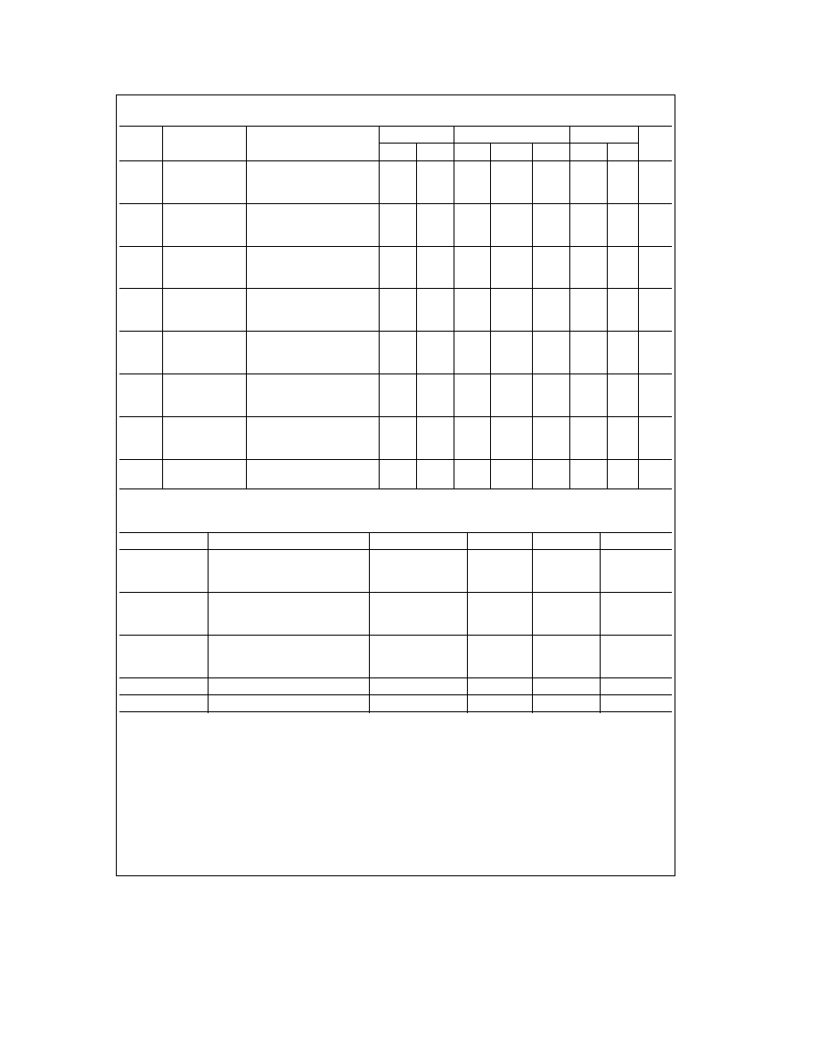
DC Electrical Characteristics
CD4071BC CD4081BC (Note 2)
Symbol
Parameter
Conditions
b
40 C
a
25 C
a
85 C
Units
Min
Max
Min
Typ
Max
Min
Max
I
DD
Quiescent Device
V
DD
e
5V
1
0 004
1
7 5
m
A
Current
V
DD
e
10V
2
0 005
2
15
m
A
V
DD
e
15V
4
0 006
4
30
m
A
V
OL
Low Level
V
DD
e
5V
0 05
0
0 05
0 05
V
Output Voltage
V
DD
e
10V
l
I
O
l
k
1 mA
0 05
0
0 05
0 05
V
V
DD
e
15V
(
0 05
0
0 05
0 05
V
V
OH
High Level
V
DD
e
5V
4 95
4 95
5
4 95
V
Output Voltage
V
DD
e
10V
l
I
O
l
k
1 mA
9 95
9 95
10
9 95
V
V
DD
e
15V
(
14 95
14 95
15
14 95
V
V
IL
Low Level
V
DD
e
5V V
O
e
0 5V
1 5
2
1 5
1 5
V
Input Voltage
V
DD
e
10V V
O
e
1 0V
3 0
4
3 0
3 0
V
V
DD
e
15V V
O
e
1 5V
4 0
6
4 0
4 0
V
V
IH
High Level
V
DD
e
5V V
O
e
4 5V
3 5
3 5
3
3 5
V
Input Voltage
V
DD
e
10V V
O
e
9 0V
7 0
7 0
6
7 0
V
V
DD
e
15V V
O
e
13 5V
11 0
11 0
9
11 0
V
I
OL
Low Level Output
V
DD
e
5V V
O
e
0 4V
0 52
0 44
0 88
0 36
mA
Current
V
DD
e
10V V
O
e
0 5V
1 3
1 1
2 25
0 9
mA
(Note 3)
V
DD
e
15V V
O
e
1 5V
3 6
3 0
8 8
2 4
mA
I
OH
High Level Output
V
DD
e
5V V
O
e
4 6V
b
0 52
b
0 44
b
0 88
b
0 36
mA
Current
V
DD
e
10V V
O
e
9 5V
b
1 3
b
1 1
b
2 25
b
0 9
mA
(Note 3)
V
DD
e
15V V
O
e
13 5V
b
3 6
b
3 0
b
8 8
b
2 4
mA
I
IN
Input Current
V
DD
e
15V V
IN
e
0V
b
0 30
b
10
b
5
b
0 30
b
1 0
m
A
V
DD
e
15V V
IN
e
15V
0 30
10
b
5
0 30
1 0
m
A
AC Electrical Characteristics
CD4071BC CD4071BM
T
A
e
25 C Input t
r
t
f
e
20 ns C
L
e
50 pF R
L
e
200 kX Typical temperature coefficient is 0 3% C
Symbol
Parameter
Conditions
Typ
Max
Units
t
PHL
Propagation Delay Time
V
DD
e
5V
100
250
ns
High-to-Low Level
V
DD
e
10V
40
100
ns
V
DD
e
15V
30
70
ns
t
PLH
Propagation Delay Time
V
DD
e
5V
90
250
ns
Low-to-High Level
V
DD
e
10V
40
100
ns
V
DD
e
15V
30
70
ns
t
THL
t
TLH
Transition Time
V
DD
e
5V
90
200
ns
V
DD
e
10V
50
100
ns
V
DD
e
15V
40
80
ns
C
IN
Average Input Capacitance
Any Input
5
7 5
pF
C
PD
Power Dissipation Capacity
Any Gate
18
pF
AC Parameters are guaranteed by DC correlated testing
Note 1
``Absolute Maximum Ratings'' are those values beyond which the safety of the device cannot be guaranteed Except for ``Operating Temperature Range''
they are not meant to imply that the devices should be operated at these limits The table of ``Electrical Characteristics'' provides conditions for actual device
operation
Note 2
All voltages measured with respect to V
SS
unless otherwise specified
Note 3
I
OH
and I
OL
are tested one output at a time
3
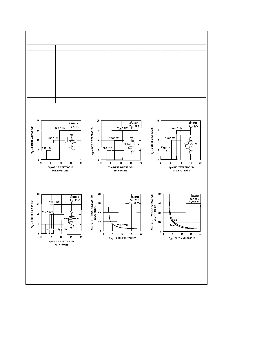
AC Electrical Characteristics
CD4081BC CD4081BM
T
A
e
25 C Input t
r
t
f
e
20 ns C
L
e
50 pF R
L
e
200 kX Typical temperature coefficient is 0 3% C
Symbol
Parameter
Conditions
Typ
Max
Units
t
PHL
Propagation Delay Time
V
DD
e
5V
100
250
ns
High-to-Low Level
V
DD
e
10V
40
100
ns
V
DD
e
15V
30
70
ns
t
PLH
Propagation Delay Time
V
DD
e
5V
120
250
ns
Low-to-High Level
V
DD
e
10V
50
100
ns
V
DD
e
15V
35
70
ns
t
THL
t
TLH
Transition Time
V
DD
e
5V
90
200
ns
V
DD
e
10V
50
100
ns
V
DD
e
15V
40
80
ns
C
IN
Average Input Capacitance
Any Input
5
7 5
pF
C
PD
Power Dissipation Capacity
Any Gate
18
pF
AC Parameters are guaranteed by DC correlated testing
Typical Performance Characteristics
TL F 5977 ≠ 7
FIGURE 1 Typical Transfer
Characteristics
TL F 5977 ≠ 8
FIGURE 2 Typical Transfer
Characteristics
TL F 5977 ≠ 9
FIGURE 3 Typical Transfer
Characteristics
TL F 5977 ≠ 10
FIGURE 4 Typical Transfer
Characteristics
TL F 5977 ≠ 11
FIGURE 5
TL F 5977 ≠ 12
FIGURE 6
4
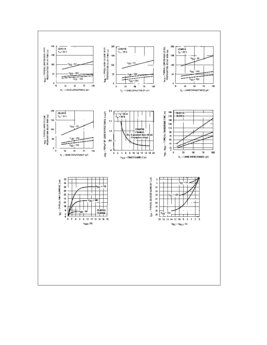
Typical Performance Characteristics
(Continued)
TL F 5977 ≠ 13
FIGURE 7
TL F 5977 ≠ 14
FIGURE 8
TL F 5977 ≠ 15
FIGURE 9
TL F 5977 ≠ 16
FIGURE 10
TL F 5977 ≠ 17
FIGURE 11
TL F 5977 ≠ 18
FIGURE 12
TL F 5977 ≠ 19
FIGURE 13
TL F 5977 ≠ 20
FIGURE 14
5