
TL F 6000
CD4538BMCD4538BC
Dual
Precision
Monostable
February 1988
CD4538BM CD4538BC Dual Precision Monostable
General Description
The CD4538B is a dual precision monostable multivibrator
with independent trigger and reset controls The device is
retriggerable and resettable and the control inputs are inter-
nally latched Two trigger inputs are provided to allow either
rising or falling edge triggering The reset inputs are active
low and prevent triggering while active Precise control of
output pulse-width has been achieved using linear CMOS
techniques The pulse duration and accuracy are deter-
mined by external components R
X
and C
X
The device does
not allow the timing capacitor to discharge through the tim-
ing pin on power-down condition For this reason no exter-
nal protection resistor is required in series with the timing
pin Input protection from static discharge is provided on all
pins
Features
Y
Wide supply voltage range
3 0V to 15V
Y
High noise immunity
0 45 V
CC
(typ )
Y
Low power
Fan out of 2 driving 74L
TTL compatibility
or 1 driving 74LS
Y
New formula PW
OUT
e
RC
(PW in seconds R in Ohms C in Farads)
Y
g
1 0% pulse-width variation from part to part (typ )
Y
Wide pulse-width range
1 ms to %
Y
Separate latched reset inputs
Y
Symmetrical output sink and source capability
Y
Low standby current
5 nA (typ )
5 V
DC
Y
Pin compatible to CD4528B
Block and Connection Diagrams
TL F 6000 � 1
R
X
and C
X
are External Components
V
DD
e
Pin 16
V
SS
e
Pin 8
Dual-In-Line Package
CD4538BM
CD4538BC
TL F 6000 � 2
Top View
Order Number CD4538B
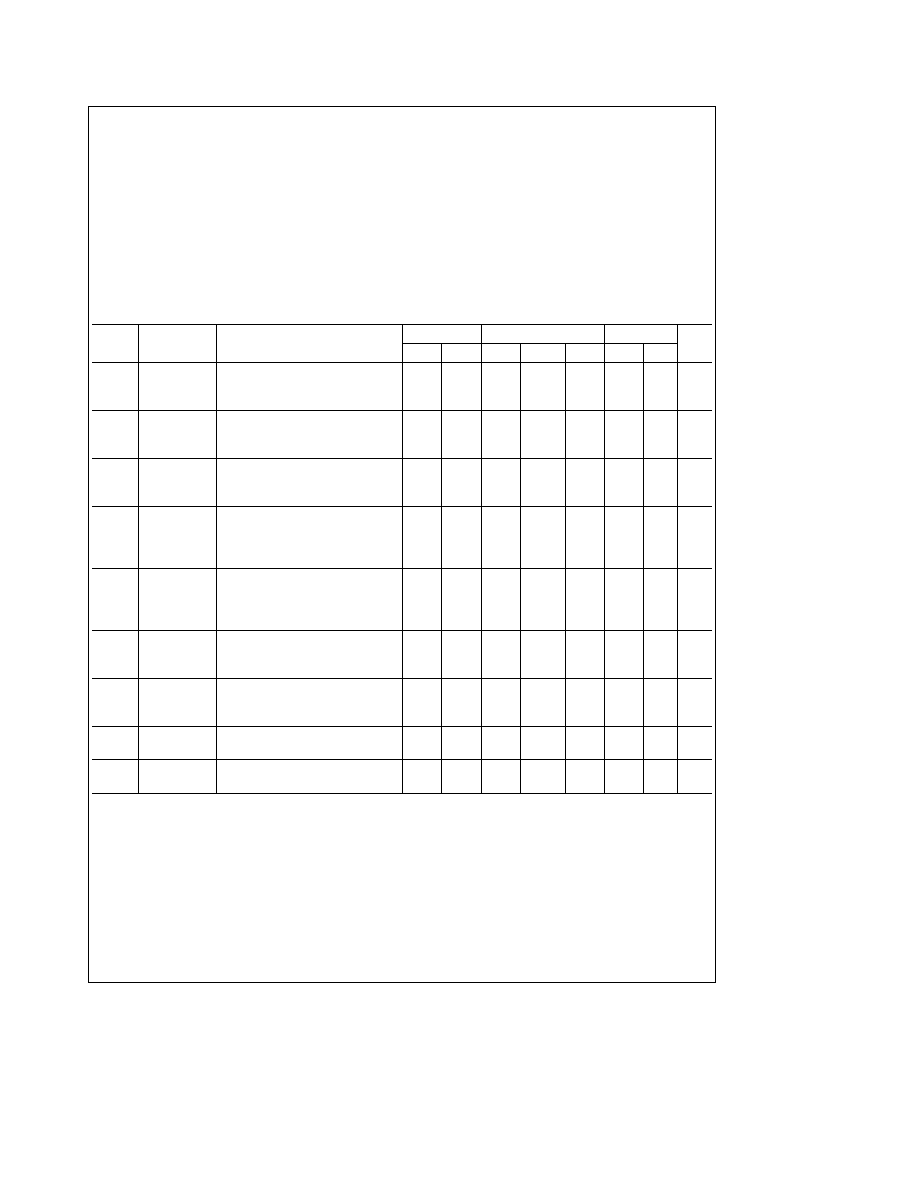
Truth Table
Inputs
Outputs
Clear
A
B
Q
Q
L
X
X
L
H
X
H
X
L
H
X
X
L
L
H
H
L
v
H
u
H
H
e
High Level
L
e
Low Level
u
e
Transition from Low to High
v
e
Transition from High to Low
e
One High Level Pulse
e
One Low Level Pulse
X
e
Irrelevant
C1995 National Semiconductor Corporation
RRD-B30M105 Printed in U S A
Absolute Maximum Ratings
(Notes 1 and 2)
If Military Aerospace specified devices are required
please contact the National Semiconductor Sales
Office Distributors for availability and specifications
DC Supply Voltage (V
DD
)
b
0 5 to
a
18 V
DC
Input Voltage (V
IN
)
b
0 5V to V
DD
a
0 5 V
DC
Storage Temperature Range (T
S
)
b
65 C to
a
150 C
Power Dissipation (P
D
)
Dual-In-Line
700 mW
Small Outline
500 mW
Lead Temperature (T
L
)
(Soldering 10 seconds)
260 C
Recommended Operating
Conditions
(Note 2)
DC Supply Voltage (V
DD
)
3 to 15 V
DC
Input Voltage (V
IN
)
0 to V
DD
V
DC
Operating Temperature Range (T
A
)
CD4538BM
b
55 C to
a
125 C
CD4538BC
b
40 C to
a
85 C
DC Electrical Characteristics
CD4538BM (Note 2)
Symbol
Parameter
Conditions
b
55 C
a
25 C
a
125 C
Units
Min
Max
Min
Typ
Max
Min
Max
I
DD
Quiescent
V
DD
e
5V
V
IH
e
V
DD
5
0 005
5
150
m
A
Device Current V
DD
e
10V
V
IL
e
V
SS
10
0 010
10
300
m
A
V
DD
e
15V
(
All Outputs Open
20
0 015
20
600
m
A
V
OL
Low Level
V
DD
e
5V
l
I
O
l
k
1 mA
0 05
0
0 05
0 05
V
Output Voltage V
DD
e
10V
V
IH
e
V
DD
V
IL
e
V
SS
0 05
0
0 05
0 05
V
V
DD
e
15V
(
0 05
0
0 05
0 05
V
V
OH
High Level
V
DD
e
5V
l
I
O
l
k
1 mA
4 95
4 95
5
4 95
V
Output Voltage V
DD
e
10V
V
IH
e
V
DD
V
IL
e
V
SS
9 95
9 95
10
9 95
V
V
DD
e
15V
(
14 95
14 95
15
14 95
V
V
IL
Low Level
l
I
O
l
k
1 mA
Input Voltage
V
DD
e
5V V
O
e
0 5V or 4 5V
1 5
2 25
1 5
1 5
V
V
DD
e
10V V
O
e
1 0V or 9 0V
3 0
4 50
3 0
3 0
V
V
DD
e
15V V
O
e
1 5V or 13 5V
4 0
6 75
4 0
4 0
V
V
IH
High Level
l
I
O
l
k
1 mA
Input Voltage
V
DD
e
5V V
O
e
0 5V or 4 5V
3 5
3 5
2 75
3 5
V
V
DD
e
10V V
O
e
1 0V or 9 0V
7 0
7 0
5 50
7 0
V
V
DD
e
15V V
O
e
1 5V or 13 5V
11 0
11 0
8 25
11 0
V
I
OL
Low Level
V
DD
e
5V V
O
e
0 4V
V
IH
e
V
DD
0 64
0 51
0 88
0 36
mA
Output Current
V
DD
e
10V V
O
e
0 5V
V
IL
e
V
SS
1 6
1 3
2 25
0 9
mA
(Note 3)
V
D
e
15V V
O
e
1 5V
(
4 2
3 4
8 8
2 4
mA
I
OH
High Level
V
DD
e
5V V
O
e
4 6V
V
IH
e
V
DD
b
0 64
b
0 51
b
0 88
b
0 36
mA
Output Current
V
DD
e
10V V
O
e
9 5V
V
IL
e
V
SS
b
1 6
b
1 3
b
2 25
b
0 9
mA
(Note 3)
V
D
e
15V V
O
e
13 5V
(
b
4 2
b
3 4
b
8 8
b
2 4
mA
I
IN
Input Current
V
DD
e
15V V
IN
e
0V or 15V
g
0 02
g
10
b
5
g
0 05
g
0 5
m
A
Pin 2 or 14
I
IN
Input Current
V
DD
e
15V V
IN
e
0V or 15V
g
0 1
g
10
b
5
g
0 1
g
1 0
m
A
Other Inputs
Note 1
``Absolute Maximum Ratings'' are those values beyond which the safety of the device cannot be guaranteed they are not meant to imply that the devices
should be operated at these limits The tables of ``Recommended Operating Conditions'' and ``Electrical Characteristics'' provide conditions for acutal device
operation
Note 2
V
SS
e
0V unless otherwise specified
Note 3
I
OH
and I
OL
are tested one output at a time
2

DC Electrical Characteristics
CD4538BC (Note 2)
Symbol
Parameter
Conditions
b
40 C
a
25 C
a
85 C
Units
Min
Max
Min
Typ
Max
Min
Max
I
DD
Quiescent
V
DD
e
5V
V
IH
e
V
DD
20
0 005
20
150
m
A
Device Current V
DD
e
10V
V
IL
e
V
SS
40
0 010
40
300
m
A
V
DD
e
15V
(
All Outputs Open
80
0 015
80
600
m
A
V
OL
Low Level
V
DD
e
5V
l
I
O
l
k
1 mA
0 05
0
0 05
0 05
V
Output Voltage V
DD
e
10V
V
IH
e
V
DD
V
IL
e
V
SS
0 05
0
0 05
0 05
V
V
DD
e
15V
(
0 05
0
0 05
0 05
V
V
OH
High Level
V
DD
e
5V
l
I
O
l
k
1 mA
4 95
4 95
5
4 95
V
Output Voltage V
DD
e
10V
V
IH
e
V
DD
V
IL
e
V
SS
9 95
9 95
10
9 95
V
V
DD
e
15V
(
14 95
14 95
15
14 95
V
V
IL
Low Level
l
I
O
l
k
1 mA
Input Voltage
V
DD
e
5V V
O
e
0 5V or 4 5V
1 5
2 25
1 5
1 5
V
V
DD
e
10V V
O
e
1 0V or 9 0V
3 0
4 50
3 0
3 0
V
V
DD
e
15V V
O
e
1 5V or 13 5V
4 0
6 75
4 0
4 0
V
V
IH
High Level
l
I
O
l
k
1 mA
Input Voltage
V
DD
e
5V V
O
e
0 5V or 4 5V
3 5
3 5
2 75
3 5
V
V
DD
e
10V V
O
e
1 0V or 9 0V
7 0
7 0
5 50
7 0
V
V
DD
e
15V V
O
e
1 5V or 13 5V
11 0
11 0
8 25
11 0
V
I
OL
Low Level
V
DD
e
5V V
O
e
0 4V
V
IH
e
V
DD
0 52
0 44
0 88
0 36
mA
Output Current
V
DD
e
10V V
O
e
0 5V
V
IL
e
V
SS
1 3
1 1
2 25
0 9
mA
(Note 3)
V
D
e
15V V
O
e
1 5V
(
3 6
3 0
8 8
2 4
mA
I
OH
High Level
V
DD
e
5V V
O
e
4 6V
b
0 52
b
0 44
b
0 88
b
0 36
mA
Output Current
V
DD
e
10V V
O
e
9 5V
V
IL
e
V
SS
b
1 3
b
1 1
b
2 25
b
0 9
mA
(Note 3)
V
D
e
15V V
O
e
13 5V
(
b
3 6
b
3 0
b
8 8
b
2 4
mA
I
IN
Input Current
V
DD
e
15V V
IN
e
0V or 15V
g
0 02
g
10
b
5
g
0 05
g
0 5
m
A
Pin 2 or 14
I
IN
Input Current
V
DD
e
15V V
IN
e
0V or 15V
g
0 3
g
10
b
5
g
0 3
g
1 0
m
A
Other Inputs
Note 1
``Absolute Maximum Ratings'' are those values beyond which the safety of the device cannot be guaranteed they are not meant to imply that the devices
should be operated at these limits The tables of ``Recommended Operating Conditions'' and ``Electrical Characteristics'' provide conditions for acutal device
operation
Note 2
V
SS
e
0V unless otherwise specified
Note 3
I
OH
and I
OL
are tested one output at a time
3
AC Electrical Characteristics
T
A
e
25 C C
L
e
50 pF and t
r
e
t
f
e
20 ns unless otherwise specified
Symbol
Parameter
Conditions
Min
Typ
Max
Units
t
TLH
t
THL
Output Transition Time
V
DD
e
5V
100
200
ns
V
DD
e
10V
50
100
ns
V
DD
e
15V
40
80
ns
t
PLH
t
PHL
Propagation Delay Time
Trigger Operation
A or B to Q or Q
V
DD
e
5V
300
600
ns
V
DD
e
10V
150
300
ns
V
DD
e
15V
100
220
ns
Reset Operation
C
D
to Q or Q
V
DD
e
5V
250
500
ns
V
DD
e
10V
125
250
ns
V
DD
e
15V
95
190
ns
t
WL
t
WH
Minimum Input Pulse Width
V
DD
e
5V
35
70
ns
A B or C
D
V
DD
e
10V
30
60
ns
V
DD
e
15V
25
50
ns
t
RR
Minimum Retrigger Time
V
DD
e
5V
0
ns
V
DD
e
10V
0
0
ns
V
DD
e
15V
0
ns
C
IN
Input Capacitance
Pin 2 or 14
10
pF
Other Inputs
5
7 5
pF
PW
OUT
Output Pulse Width (Q or Q)
R
X
e
100 kX
V
DD
e
5V
208
226
244
m
s
(Note For Typical Distribution
C
X
e
0 002 mF
V
DD
e
10V
211
230
248
m
s
see
Figure 9 )
V
DD
e
15V
216
235
254
m
s
R
X
e
100 kX
V
DD
e
5V
8 83
9 60
10 37
ms
C
X
e
0 1 mF
V
DD
e
10V
9 02
9 80
10 59
ms
V
DD
e
15V
9 20
10 00
10 80
ms
R
X
e
100 kX
V
DD
e
5V
0 87
0 95
1 03
s
C
X
e
10 0 mF
V
DD
e
10V
0 89
0 97
1 05
s
V
DD
e
15V
0 91
0 99
1 07
s
Pulse Width Match between
R
X
e
100 kX
V
DD
e
5V
g
1
%
Circuits in the Same Package
C
X
e
0 1 mF
V
DD
e
10V
g
1
%
C
X
e
0 1 mF R
X
e
100 kX
V
DD
e
15V
g
1
%
Operating Conditions
R
X
External Timing Resistance
5 0
kX
C
X
External Timing Capacitance
0
No Limit
pF
AC parameters are guaranteed by DC correlated testing
The maximum usable resistance R
X
is a function of the leakage of the Capacitor C
X
leakage of the CD4538B and leakage due to board layout surface
resistance etc
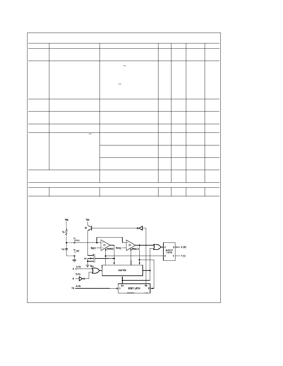
Logic Diagram
TL F 6000 � 3
FIGURE 1
4

Theory of Operation
TL F 6000 � 4
FIGURE 2
Trigger Operation
The block diagram of the CD4538B is shown in
Figure 1
with circuit operation following
As shown in
Figures 1 and 2 before an input trigger occurs
the monostable is in the quiescent state with the Q output
low and the timing capacitor C
X
completely charged to
V
DD
When the trigger input A goes from V
SS
to V
DD
(while
inputs B and C
D
are held to V
DD
) a valid trigger is recog-
nized which turns on comparator C1 and N-Channel tran-
sistor N1
j
At the same time the output latch is set With
transistor N1 on the capacitor C
X
rapidly discharges toward
V
SS
until V
REF1
is reached At this point the output of com-
parator C1 changes state and transistor N1 turns off Com-
parator C1 then turns off while at the same time comparator
C2 turns on With transistor N1 off the capacitor C
X
begins
to charge through the timing resistor R
X
toward V
DD
When
the voltage across C
X
equals V
REF2
comparator C2 chang-
es state causing the output latch to reset (Q goes low) while
at the same time disabling comparator C2 This ends the
timing cycle with the monostable in the quiescent state
waiting for the next trigger
A valid trigger is also recognized when trigger input B goes
from V
DD
to V
SS
(while input A is at V
SS
and input C
D
is at
V
DD
)
k
It should be noted that in the quiescent state C
X
is fully
charged to V
DD
causing the current through resistor R
X
to
be zero Both comparators are ``off'' with the total device
current due only to reverse junction leakages An added
feature of the CD4538B is that the output latch is set
via the input trigger without regard to the capacitor voltage
Thus propagation delay from trigger to Q is independent of
the value of C
X
R
X
or the duty cycle of the input waveform
Retrigger Operation
The CD4538B is retriggered if a valid trigger occurs
l
fol-
lowed by another valid trigger
m
before the Q output has
returned to the quiescent (zero) state Any retrigger after
the timing node voltage at pin 2 or 14 has begun to rise from
V
REF1
but has not yet reached V
REF2
will cause an in-
crease in output pulse width T When a valid retrigger is
initiated
m
the voltage at T2 will again drop to V
REF1
before
progressing along the RC charging curve toward V
DD
The
Q output will remain high until time T after the last valid
retrigger
Reset Operation
The CD4538B may be reset during the generation of the
output pulse In the reset mode of operation an input pulse
on C
D
sets the reset latch and causes the capacitor to be
fast charged to V
DD
by turning on transistor Q1
n
When
the voltage on the capacitor reaches V
REF2
the reset latch
will clear and then be ready to accept another pulse If the
C
D
input is held low any trigger inputs that occur will be
inhibited and the Q and Q outputs of the output latch will not
change Since the Q output is reset when an input low level
is detected on the C
D
input the output pulse T can be made
significantly shorter than the minimum pulse width specifica-
tion
5