 | –≠–ª–µ–∫—Ç—Ä–æ–Ω–Ω—ã–π –∫–æ–º–ø–æ–Ω–µ–Ω—Ç: CGS2536TV | –°–∫–∞—á–∞—Ç—å:  PDF PDF  ZIP ZIP |
TL F 12325
CGS2536V
Commercial
Quad
1
t
o
4
Clock
Drivers
CGS2536TV
Industrial
Quad
1
t
o
4
Clock
Drivers
September 1995
CGS2536V
Commercial Quad 1 to 4 Clock Drivers
CGS2536TV
Industrial Quad 1 to 4 Clock Drivers
General Description
These Clock Generation and Support clock drivers are spe-
cifically designed for driving memory arrays requiring large
fanouts while operating at high speeds
This device meets the rise and fall time requirements of the
90 MHz and 100 MHz Pentium
TM
procrssors
The CGS2536 I O structures are CMOS The outputs are
separated into two banks of eight One bank consists of
divide by two outputs the other straight-through buffers
Within each bank half the outputs are inverting the other
half non-inverting
The CGS2536 specification guarantees part-to-part skew
variation
Features
Y
Guaranteed
1 0 ns rise and fall times while driving 12 inches of
50X microstrip terminated with 25 pF
350 ps pin-to-pin skew (t
OSLH
and t
OSHL
)
Y
650 ps part-to-part variation on positive or negative
transition
Y
Operates with either 3 3V or 5 0V supply
Y
Inputs 5V tolerant with V
CC
in 3 3V range
Y
Symmetric output current drive 24 mA I
OH
I
OL
Y
Industrial temperature of
b
40 C to
a
85 C
Y
Symmetric package orientation
Y
Large fanout for memory driving applications
Y
Guaranteed 2 kV ESD protection
Y
Implemented on National's ABT family process
Y
28-pin PLCC for optimum skew performance
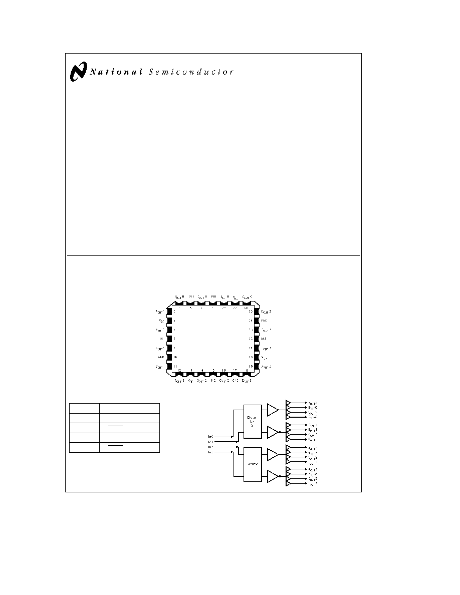
Connection Diagrams
Pin Assignment for 28-Pin PLCC
TL F 12325 ≠ 1
Truth Table
Input
Output
In 0
ABCD Out (0)
d
2
In 1
ABCD Out (1)
d
2
In 2
ABCD Out (2)
In 3
ABCD Out (3)
CGS2536
TL F 12325 ≠ 2
Pentium
TM
is a trademark of Intel Corporation
C1995 National Semiconductor Corporation
RRD-B30M105 Printed in U S A
Absolute Maximum Ratings
(Note)
If Military Aerospace specified devices are required
please contact the National Semiconductor Sales
Office Distributors for availability and specifications
Supply Voltage (V
CC
)
7 0V
Input Voltage (V
I
)
7 0V
Input Current
b
30 mA
Current Applied to Output
(High Low)
Twice the Rated IOH IOL
Operating Temperature
Industrial Grade
b
40 C to
a
85 C
Commercial grade
0 C to
a
70 C
Storage Temperature Range
b
65 C to
a
150 C
Airflow
Typical i
JA
0 LFM
62 C W
225 LFM
43 C W
500 LFM
34 C W
900 LFM
27 C W
Recommended Operating
Conditions
Supply Voltage
V
CC
4 5V to 5 5V
V
CC
3 0V to 3 6V
Maximum Input Rise Fall Time (0 8V to 2 0V)
5 ns
Free Air Operating Temperature
Commercial
0 C to
a
70 C
Industrial
b
40 C to
a
85 C
Note
The Absolute Maximum Ratings are those values beyond which the
safety of the device cannot be guaranteed The device should not be operat-
ed at these limits The parametric values defined in the DC and AC Electrical
Characteristics tables are not guaranteed at the absolute maximum ratings
The Recommended Operating Conditions will define the conditions for actu-
al device operation
DC Electrical Characteristics
Over recommended operating free air temperature range All typical values are measured at V
CC
e
5V T
A
e
25 C
Symbol
Parameter
Conditions
V
CC
Min
Typ
Max
Units
(V)
V
IH
Input High Level Voltage
3 0
2 1
V
4 5
3 15
5 5
3 85
V
IL
Input Low Level Voltage
3 0
0 9
V
4 5
1 35
5 5
1 65
V
IK
Input Clamp Voltage
I
I
e b
18 mA
4 5
b
1 2
V
V
OH
High Level Output Voltage
I
OH
e b
50 mA
3 0
2 9
V
4 5
4 4
5 5
5 4
I
OH
e b
24 mA
3 0
2 46
V
4 5
3 76
5 5
4 76
V
OL
Low Level Output Voltage
I
OL
e
50 mA
3 0
0 1
V
4 5
0 1
5 5
0 1
I
OL
e
24 mA
3 0
0 44
V
4 5
0 44
5 5
0 44
I
I
Input Current
Max Input Voltage
V
IH
e
7V
5 5
7
m
A
V
IH
e
V
CC
3 6
1
I
IH
High Level Input Current
V
IH
e
V
CC
5 5
5
m
A
I
IL
Low Level Input Current
V
IL
e
0V
5 5
b
5
m
A
I
OLD
Minimum Dynamic Output Current
V
OLD
e
1 65V (max)
5 5
75
mA
V
OLD
e
0 9V (max)
3 0
36
I
OHD
Minimum Dynamic Output Current
V
OHD
e
3 85V (min)
5 5
b
75
mA
V
OHD
e
2 1V (min)
3 0
b
25
I
CC
Supply Current
3 6
75
m
A
5 5
235
C
IN
Input Capacitance
5 0
5
pF
Maximum test duration 2 0 ms one output loaded at a time
At V
CC
e
3 3V I
OLD
e
55 mA min
V
CC
e
3 6V I
OLD
e
64 mA min
At V
CC
e
3 3V I
OHD
e b
58 mA min
V
CC
e
3 6V I
OHD
e b
66 mA min
2
AC Electrical Characteristics
(Notes 1 2 and 3)
Over recommended operating free air temperature range All typical values are measured at V
CC
e
5V T
A
e
25 C
Symbol
Parameter
CGS2536
Units
V
CC
T
A
e a
25 C
T
A
e b
40 C to
a
85 C
(V)
C
L
e
50 pF R
L
e
500X
(Note 4)
(Note 8)
C
L
e
50 pF R
L
e
500X
Min
Typ
Max
Min
Typ
Max
f
max
Frequency Maximum
3 0
100
MHz
5 0
125
t
PLH
Low-to-High Propagation Delay
3 3
7 25
7 25
ns
CK to O
n
5 0
5 0
5 0
t
PHL
High-to-Low Propagation Delay
3 3
5 5
5 5
ns
CK to O
n
5 0
4 5
4 5
t
OSLH
Maximum Skew Common Edge
3 3
150
350
300
350
ps
Output-to-Output Variation (Notes 1 3)
5 0
150
350
300
350
t
OSHL
Maximum Skew Common Edge
3 3
150
350
300
350
ps
Output-to-Output Variation (Notes 1 3)
5 0
150
350
300
350
t
rise
Rise Fall Time
3 3
4 5
4 5
ns
t
fall
(from 0 8V 2 0V to 2 0V 0 8V) (Note 5)
5 0
3 5
3 5
t
rise
Rise Fall Time
3 3
0 8
1 0
ns
t
fall
(from 0 8V 2 0V to 2 0V 0 8V) (Note 6)
5 0
0 4
0 6
t
rise
Rise Fall Time
3 3
1 0
1 0
ns
t
fall
(from 0 8V 2 0V to 2 0V 0 8V) (Note 7)
5 0
0 7
0 9
t
High
Pulse Width Duration High (Notes 2 3)
3 3
4 0
4 0
ns
5 0
4 0
4 0
t
Low
Pulse Width Duration Low (Notes 2 3)
3 3
4 0
4 0
5 0
4 0
4 0
t
PVLH
Part-to-Part Variation of
3 3
650
650
ps
Low-to-High Transitions
5 0
650
650
t
PVHL
Part-to-Part Variation of
3 3
650
650
High-to-Low Transitions
5 0
650
650
Note 1
Output-to-Output Skew is defined as the absolute value of the difference between the actual propagation delay for any outputs within the same packaged
device The specifications apply to any outputs switching in the same direction either LOW to HIGH (t
OSLH
) or HIGH to LOW (t
OSHL
)
Note 2
Time high is measured with outputs at 2 0V or above Time low is measured with outputs at 0 8V or below Input waveform characteristics for t
High
t
Low
measurement f
e
66 67 MHz duty cycle
e
50%
Note 3
The input waveform has a rise and fall time transition time of 2 5 ns (10% to 90%)
Note 4
Industrial range (
b
40 C to
a
85 C) limits apply to the commercial temperature range (0 C to
a
70 C)
Note 5
These Rise and Fall times are measured with C
L
e
50 pF R
L
e
500X (see
Figure 3 )
Note 6
These Rise and Fall times are measured with C
L
e
25 pF R
L
e
500X (see
Figure 3 ) and are guaranteed by design
Note 7
These Rise and Fall times are measured driving 12 inches of 50X microstrip terminated with equivalent C
L
e
25 pF (see
Figure 4 ) and are guaranteed by
design
Note 8
Voltage Range 5 0 is 5 0V
g
0 5V 3 3 is 3 3V
g
0 3V
Note 9
For increased output drive output pins may be connected together when the corresponding input pins are connected together
3
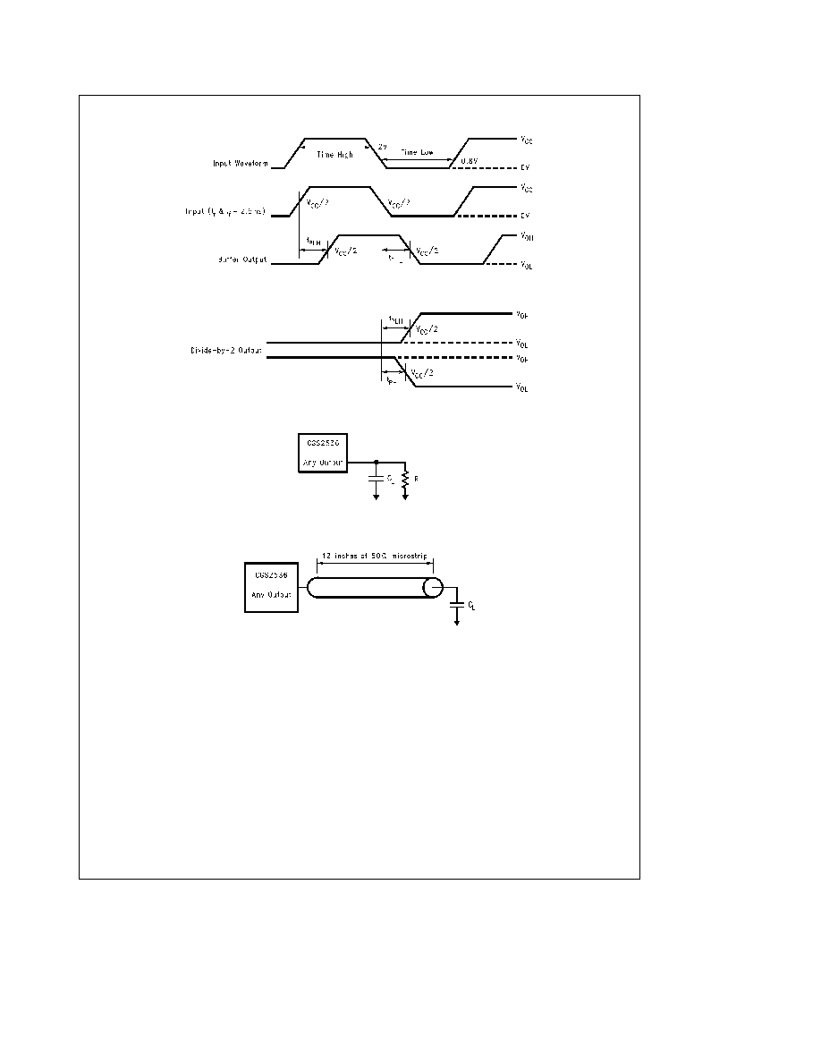
Timing Information
TL F 12325 ≠ 3
FIGURE 1 Buffer Waveforms
TL F 12325 ≠ 6
FIGURE 2 Divide by 2 Waveforms
TL F 12325 ≠ 8
FIGURE 3 A C Load (Reference Notes 5 6)
C
L
e
Total Load Including Probes
TL F 12325 ≠ 9
FIGURE 4 A C Load (Reference Note 7)
C
L
e
Total Load Including Probes
4
Power On Requirements
DETAILED DESCRIPTION
The divide by two block of the CGS2536 is accomplished
using two negative-edge-triggered flip-flops During power-
on the inverting flip-flop causes outputs Aout1 through
Dout1 to be High The non-inverting flip-flop causes outputs
Aout0 through Dout0 to be Low Two flip-flops are used to
achieve minimum skew between the non-inverting and in-
verting outputs
To guarantee that the flip-flops power-up out of phase the
IN0 and IN1 pins must be held low while power is applied to
V
CC
IN0 and IN1 must remain low until V
CC
t
3V
Application Hints
In a typical user environment IN0 and IN1 inputs may be
connected common Power is applied simultaneously to the
crystal oscillator and the CGS2536 If the oscillator output
does not deliver a clean first negative-going-edge to the IN0
and IN1 inputs only one flip-flop may toggle
Even if the user delays application of V
CC
to the CGS2536
a false trigger may occur Simply gating the oscillator to the
IN0 and IN1 inputs will not guarantee correct operation
since a ``runt'' pulse may propagate through the gate and
toggle only one of the flip-flops
Figure 1 shows a circuit that delivers ``runt-free'' negative-
going-edges to the IN0 and IN1 inputs This circuit ensures
that the first clocking pulse seen by the IN0 and IN1 inputs
consists of a full positive half-cycle of the crystal oscillator
Figure 2 shows the waveforms from the synchronizing cir-
cuit
The propagation delay of the 74AC00 gates and the toggle
frequency of the 74VHC164 limit the maximum frequency of
operation Equivalent logic elements that have faster propa-
gation delays can be substituted for the NAND gates and
shift register For example a generic GAL22V10-5 could be
programmed as the NAND gates that drive the CGS2536
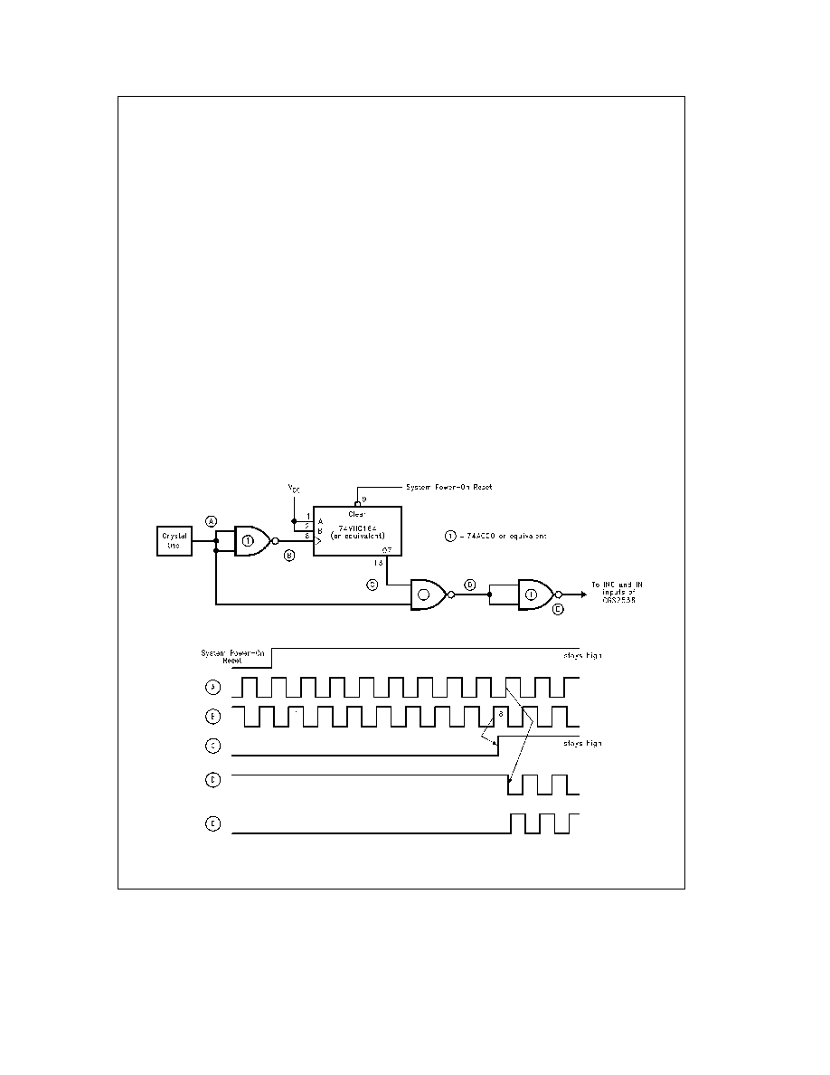
Figure 1 CIRCUIT DESCRIPTION
Assumptions
1 V
CC
is applied simultaneously to the crystal oscillator
CGS2536 74AC00 and 74VHC164
2 A system power-on reset is ``Low'' long enough for V
CC
and the crystal oscillator to stabilize
At power-on assertion (low) of the system power-on reset
clears the outputs of the 74VHC164 serial to parallel con-
verter
As a result nodes C and E are low ensuring power-on re-
quirements for the CGS2536 are met When the system
power-on reset is de-asserted the eighth positive-going-
edge received by the 74VHC164 causes node C to go high
Node C remains high as long as power is applied However
node D still remains high due to the oscillator output (A)
being low Node E stays low until the next positive-going-
edge of the oscillator Thus a full positive half-cycle of the
oscillator is seen by the IN1 and IN0 inputs which ensures
that both flip-flops of the divide by two toggle
TL F 12325 ≠ 4
TL F 12325 ≠ 5
5