 | –≠–ª–µ–∫—Ç—Ä–æ–Ω–Ω—ã–π –∫–æ–º–ø–æ–Ω–µ–Ω—Ç: CGS700V | –°–∫–∞—á–∞—Ç—å:  PDF PDF  ZIP ZIP |
TL F 11955
CGS700V
Commercial
Low
Skew
PLL
1
t
o
9
CMOS
Clock
Driver
September 1995
CGS700V
Commercial Low Skew PLL 1 to 9 CMOS Clock Driver
General Description
CGS700 is an off the shelf clock driver specifically designed
for today's high speed processors It provides low skew out-
puts which are produced at different frequencies from three
fixed input references The XTALIN input pin is designed to
be driven from three distinct crystal oscillators running at
25 MHz 33 MHz or 40 MHz
The PLL using a charge pump and an internal loop filter
multiplies this input frequency to create a maximum output
frequency of four times the input
The device includes a TRI-STATE
control pin to disable
the outputs while the PLL is still in lock This function allows
for testing the board without having to wait to acquire the
lock once the testing is complete
(continued)
Features
Y
Guaranteed and tested
500 ps pin-to-pin skew (t
OSHL
and t
OSLH
) on 1X
outputs
Y
Guaranteed
400 ps pin-to-pin skew (t
OSHL
and t
OSLH
) on
1Xoutputs
Y
Pentium
TM
and PowerPC
TM
compatible
Y
Output buffer of nine drivers for large fanout
Y
25 MHz ≠ 160 MHz output frequency range
Y
Outputs operating at 4X 2X 1X of the reference
frequency for multi-frequency bus applications
Y
Selectable output frequency
Y
TRI-STATE output control with the PLL is in the lock
state
Y
Internal loop filter to reduce noise and jitter
Y
Separate analog and digital V
CC
and Ground pins
Y
Low frequency test mode by disabling the PLL
Y
Implemented on National's Core CMOS process
Y
Symmetric output current drive
a
30 mA
b
30 mA I
OL
I
OH
Y
28-pin PCC for optimum skew performance
Y
Guaranteed 2k ESD protection
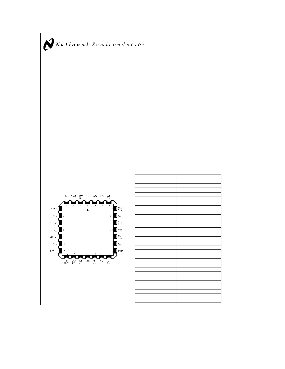
Connection Diagram
Pin Assignment for PLCC
TL F 11955 ≠ 1
See NS Package Number V28A
TRI-STATE
is a registered trademark of National Semiconductor Corporation
PowerPC
TM
is a trademark of IBM
Pentium
TM
is a trademark of Intel Corporation
Pin Description
PLCC Package
Pin
Name
Description
1
V
CC
Digital V
CC
2
SKWSEL
Skew Test Selector Pin
3
CLK4
4X Clock Output
4
V
CC
Digital V
CC
5
XTALIN
Crystal Oscillator Input
6
GND
Digital Ground
7
CLK1
0
1X Clock Output
8
V
CC
Digital V
CC
9
CLK1
1
1X Clock Output
10
GND
Digital Ground
11
CLK1
2
1X Clock Output
12
TRI-STATE
Output TRI-STATE Control
13
SKWTST
Skew Testing Pin
14
CLK1
3
1X Clock Output
15
GND
Digital Ground
16
CLK1
4
1X Clock Output
17
V
CC
Digital V
CC
18
EXTCLK
External Test Clock
19
GNDA
Analog Ground
20
V
CCA
Analog V
CC
21
EXTSEL
External Clock Mux Selector
22
GND
Digital Ground
23
CLK1
5
1X Clock Output
24
V
CC
Digital V
CC
25
CLK1
6
1X Clock Output
26
CLK1SEL
CLK1 Multiplier Selector
27
GND
Digital Ground
28
CLK2
2X Clock Output
C1996 National Semiconductor Corporation
RRD-B30M66 Printed in U S A
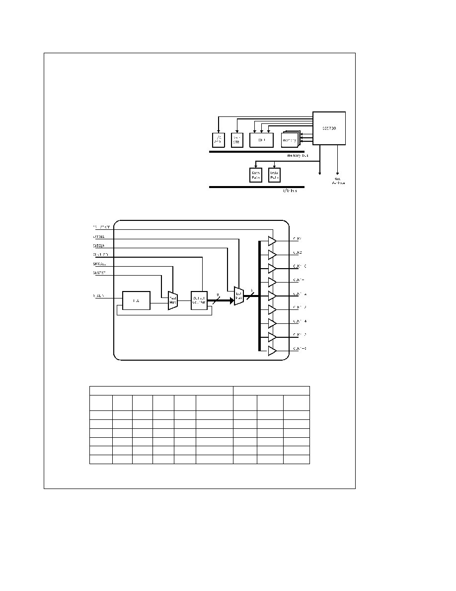
General Description
(Continued)
Also included are two EXTSEL and EXTCLK pins to allow
testing the chip via an external source The EXTSEL pin
once set to high
causes the External-Clock
Mux to
change its input from the output of the VCO and Counter to
the external clock signal provided via EXTCLK input pin
CLK1SEL pin changes the output frequency of the
CLK1
0 CLK1
6 outputs During normal operation when
CLK1SEL pin is high these outputs are at the same fre-
quency as the input crystal oscillator while CLK2 and CLK4
outputs are at twice and four times the input frequency re-
spectively
Once CLK1SEL pin is set to a low logic level the CLK1
outputs will be at twice the input frequency the same as the
CLK2 output with CLK4 output still being at four times the
input frequency
In addition two other pins are added for increasing the test
capability SKWSEL and SKWTST pins allow testing of the
counter's output and skew of the output drivers by bypass-
ing the VCO In this test mode CLK4 frequency is the same
as SKWTST input frequency while CLK2 is
and CLK1
frequencies are
respectively (refer to the truth table) In
addition CLK1SEL functionality is also true under this test
condition
Typical Application
TL F 11955 ≠ 3
Block Diagram
CGS700
TL F 11955 ≠ 2
Truth Table
Input
Output
CLK1
EXT
EXT
SKW
SKW
TRI-STATE
CLK4
CLK2
CLK1
SEL
SEL
CLK
SEL
TST
H
L
X
L
X
H
4
c
f
IN
2
c
f
IN
f
IN
L
L
X
L
X
H
4
c
f
IN
2
c
f
IN
2
c
f
IN
X
H
X
X
H
H
L
X
H
H
1
c
f
tst
c
f
tst
c
f
tst
L
L
X
H
H
1
c
f
tst
c
f
tst
c
f
tst
X
X
X
X
X
L
Z
Z
Z
Steady State phase frequency lock
http
www national com
2
CGS700
Absolute Maximum Ratings
(Note A)
If Military Aerospace specified devices are required
please contact the National Semiconductor Sales
Office Distributors for availability and specifications
Supply Voltage (V
CC
)
b
0 5V to
a
7 0V
DC Input Voltage Diode Current (I
IK
)
V
e b
0 5V
b
20 mA
V
e
V
CC
a
0 5V
a
20 mA
DC Input Voltage (V
I
)
b
0 5V to V
CC
a
0 5V
DC Output Diode Current (I
O
)
V
e b
0 5V
b
20 mA
V
e
V
CC
a
0 5V
a
20 mA
DC Output Voltage (V
O
)
b
0 5V to V
CC
a
0 5V
DC Output Source or Sink Current (I
O
)
g
60 mA
DC V
CC
or Ground Current
per Output Pin (I
CC
or I
GND
)
g
60 mA
Storage Temperature (T
STG
)
b
65 C to
a
150 C
Junction Temperature
150 C
Power Dissipation (Static and Dynamic) (Note B)
1400 mW
Note A
The Absolute Maximum Ratings are those values beyond which the
safety of the device cannot be guaranteed The device should not
be operated at these limits The parametric values defined in the
DC and AC Electrical Characteristics tables are not guaranteed at
the absolute maximum ratings The Recommended Operating Con-
ditions will define the conditions for actual device operation
Note B
Power dissipation is calculated using 49 W as the thermal coeffi-
cient for the PCC package at 225 LFM airflow The input frequency
is assumed
33 MHz with CLK4 at 132 MHz and CLK2 and CLK1's
being at 66 MHz In addition the ambient temperature is assumed
with power supply at 5 0V
Recommended Operating
Conditions
Supply Voltage (V
CC
)
4 5V to 5 5V
Input Voltage (V
I
)
0V to V
CC
Output Voltage (V
O
)
0V to V
CC
Input Crystal Frequency
25 MHz to 40 MHz
Operating Temperature (T
A
)
0 C to
a
70 C
External Clock Frequency (EXTCLK Pin)
1 MHz to 10 MHz
XTALIN Duty Cycle Range
25 75 (75 25)%
Input Rise and Fall Times (0 8V to 2 0V)
Crystal Input
5 ns max
All Other Inputs
10 ns max
Typical i
JA
0 LFM
54 C W
225 LFM
45 C W
500 LFM
38 C W
900 LFM
34 C W
DC Electrical Characteristics
Over recommended operating free air temperature range All typical values are measured at V
CC
e
5V T
A
e
25 C
Symbol
Parameter
Conditions
V
CC
e
4 5V ≠ 5 5V
Units
T
A
e
0 C ≠ 70 C
Min
Typ
Max
V
IH
Minimum Input High Level Voltage
2 0
V
V
IL
Maximum Input Low Level Voltage
0 8
V
V
OH
Minimum Output High Level Voltage
I
OUT
e b
50 mA
V
CC
b
0 1
V
I
OH
e b
30 mA
V
CC
b
0 6
V
OL
Maximum Output Low Level Voltage
I
OUT
e
50 mA
0 1
V
I
OL
e
30 mA
0 6
I
OHD
High Level Output Current
V
OH
e
V
CC
b
1 0V
50
110
170
mA
I
OLD
Low Level Output Current
V
OL
e
1 0V
50
110
170
mA
I
IN
Leakage Current
V
IN
e
0 4V or 4 6V
b
50
50
m
A
I
OZL H
Output Leakage Current
C
IN
Input Capacitance
10 0
pF
I
CC
Quiescent Digital
a
Analog Current (No Load)
V
IN
e
V
CC
GND
3 0
5 0
mA
I
CCT
I
CC
per TTL Input
V
IN
e
V
CC
b
2 1 GND
2 5
http
www national com
3
CGS700
(Continued)
AC Electrical Characteristics
Over recommended operating free air temperature range All typical values are measured at V
CC
e
5V T
A
e
25 C
Symbol
Parameter
V
CC
e
4 5V ≠ 5 5V
Units
Notes
F
IN
e
25 MHz ≠ 40 MHz
T
A
e
0 C ≠ 70 C
C
L
e
Circuit 1 and 2
R
L
e
Circuit 1 and 2
Min
Typ
Max
t
rise
Output Rise
CLK4
0 8V ≠ 2 6V
2 0
ns
(Notes 1 5)
CLK2
1 0V ≠ V
CC
b
1 0V
CLK1
1 0V ≠ V
CC
b
1 0V
ALL
0 8V ≠ 2 0V
1 5
t
fall
Output Fall
CLK4
2 6V ≠ 0 8V
2 0
ns
(Notes 1 5)
CLK2
V
CC
b
1 0V ≠ 1 0V
CLK1
V
CC
b
1 0V ≠ 1 0V
ALL
2 0V ≠ 0 8V
1 5
t
skew
Maximum Edge-
a
to
a
Edges
CLK1
CLK1
400
to-Edge Output
a
to
a
Edges
CLK1
CLK4
1000
ps
(Notes 2 5)
Skew
a
to
a
Edges
CLK2
CLK4
1000
t
lock
Time to Lock the Output to the Synch Input
100
m
s
t
cycle
Output Duty Cycle
CLK1 Outputs
49
51
%
(Notes 3 5)
CLK2 Output
49
51
CLK4 Output
35
65
J
LT
Output Jitter (Long Term)
0 3
ns
(Notes 4 5)
F
MIN
Minimum XTALIN Frequency
15
MHz
F
MAX
Maximum XTALIN Frequency
43
MHz
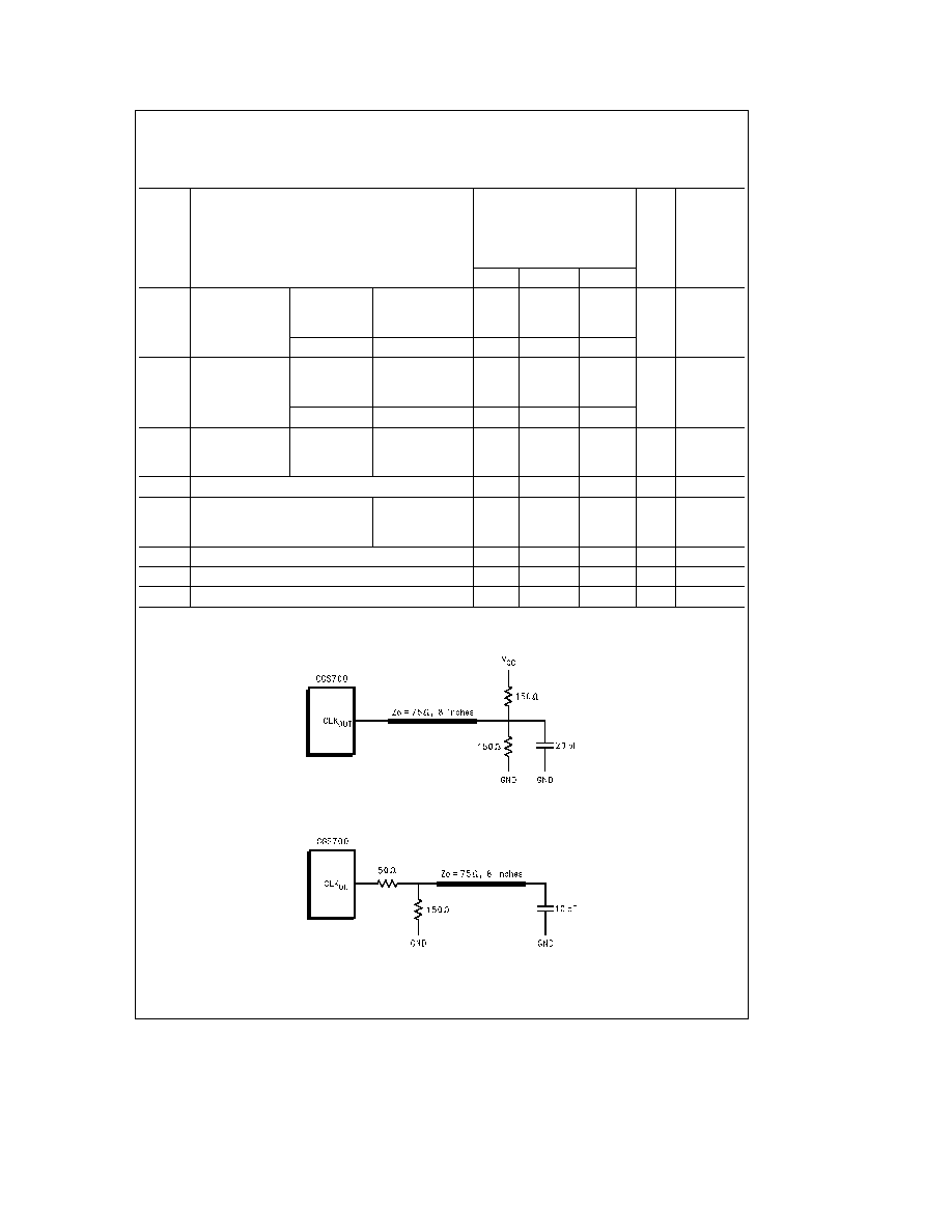
Circuit 1 Test Circuit for CLK1 and CLK2
TL F 11955 ≠ 4
Circuit 2 Test Circuit for CLK4
TL F 11955 ≠ 9
http
www national com
4
CGS700
(Continued)
Note 1
t
rise
and t
fall
parameters are measured at the pin of the device
Note 2
Skew is measured at 50% of V
CC
for CLK1 and CLK2 while it is measured
1 4V for CLK4 Limits are guaranteed by design
Note 3
Output duty cycle is measured at V
DD
2 for CLK1 and CLK2 while it is measured
1 4V for CLK4 Limits are guaranteed by design
Note 4
Jitter parameter is characterized and is guaranteed by design only It measures the uncertainty of either the positive or the negative edge over 1000
cycles It is also measured at output levels of V
CC
2 Refer to
Figure 2 for further explanation
Note 5
The GNDA pins of the 700 must be as free of noise as possible for minimum jitter Separate analog ground plane is recommended for the PCB
Also the V
CCA
pin requires extra filtering to further reduce noise Ferrite beads for filtering and bypass capacitors are suggested for V
CCA
pin
TL F 11955 ≠ 5
TL F 11955 ≠ 6
TL F 11955 ≠ 7
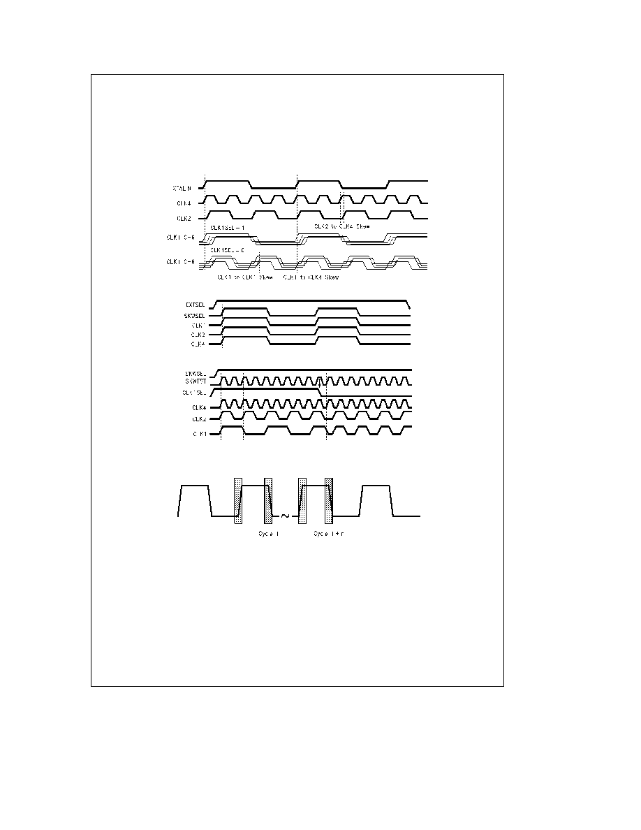
FIGURE 1 Waveforms
TL F 11955 ≠ 8
Jitter
e
l
Period(1)
b
Period(n
a
1)
l
e
300 ps for either the rising or falling edge where n is 1 to 1000 cycles
FIGURE 2 Jitter
Application References and Bibliography
Information relating to EMI as well as general application issues are in the following application notes
AN-988
EMI App Note
AN-640
AN-991
http
www national com
5