TL F 10907
CGS74B2525
1-to-8
Minimum
Skew
Clock
Driver
September 1995
CGS74B2525
1-to-8 Minimum Skew Clock Driver
General Description
This minimum skew clock driver is designed for Clock Gen-
eration and Support (CGS) applications operating well
above 20 MHz (33 MHz 50 MHz) The device guarantees
minimum output skew across the outputs of a given device
and also from device-to-device Skew parameters are also
provided as a means to measure duty cycle requirements as
those found in high speed clocking systems The 'B2525 is
a minimum skew clock driver with one input driving eight
outputs specifically designed for signal generation and clock
distribution applications
Features
Y
Clock Generation and Support (CGS) Device
Ideal for
high frequency signal generation or clock distribution
applications
Y
CGS74B version features National's Advanced Bipolar
FAST
LSI process
Y
1-to-8 low skew clock distribution
Y
600 ps pin-to-pin output skew
Y
Specifications for device-to-device variation of propaga-
tion delay
Y
Specification for transition skew to meet duty cycle
requirements
Y
Center pin V
CC
and GND configuration to minimize high
speed switching noise
Y
Current sourcing 48 mA and current sinking of 64 mA
Y
Low dynamic power consumption above 20 MHz
Y
Guaranteed 4 kV ESD protection
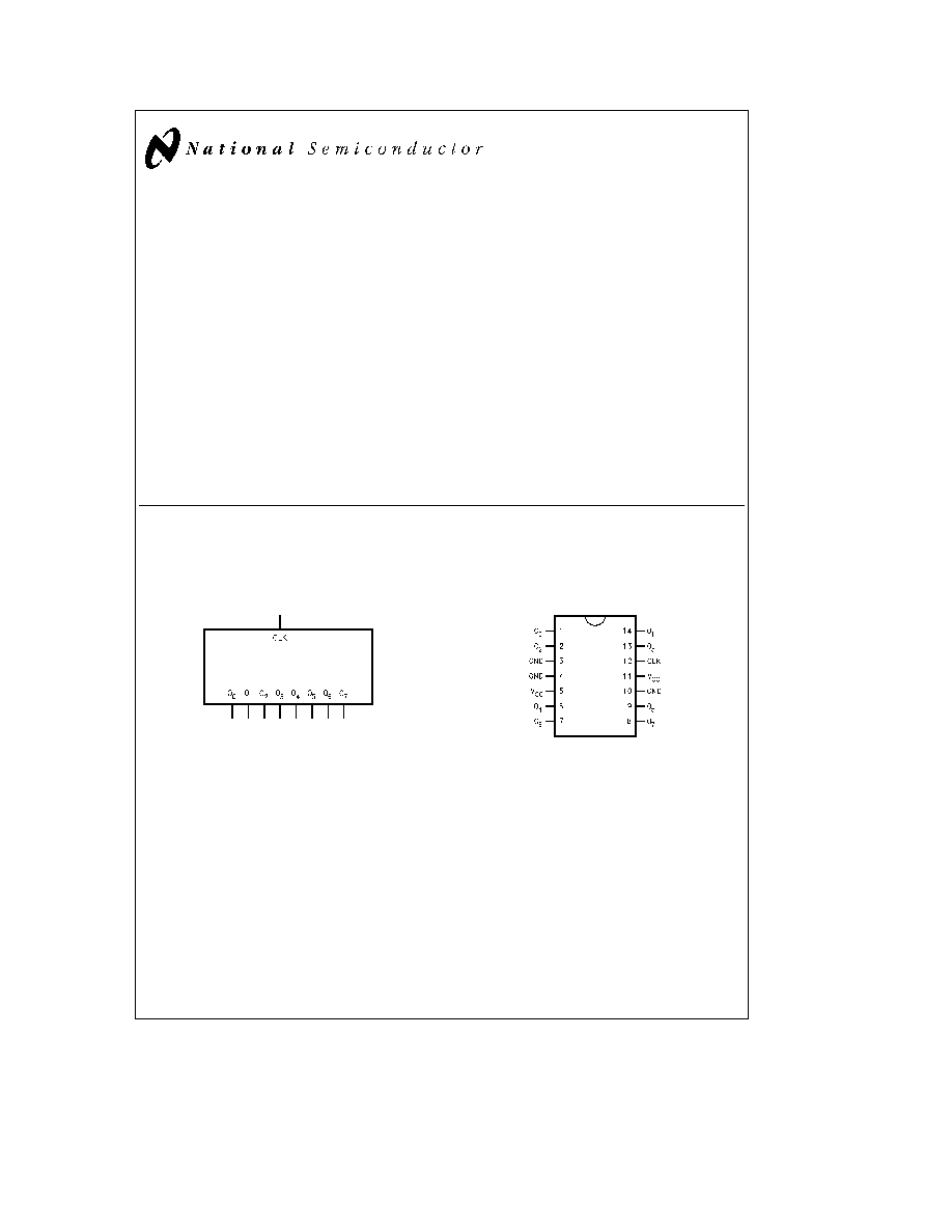
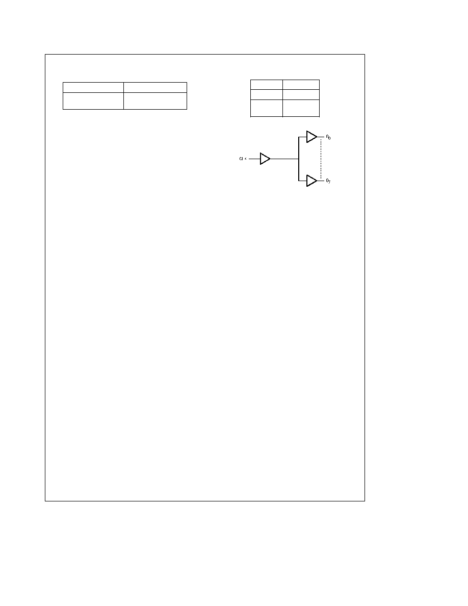
Logic Symbol
TL F 10907 ≠ 1
Connection Diagram
Pin Assignment
for DIP and SOIC
TL F 10907 ≠ 2
FAST
and TRI-STATE
are registered trademarks of National Semiconductor Corporation
C1995 National Semiconductor Corporation
RRD-B30M115 Printed in U S A
Functional Description
Pin Description
Pin Names
Description
CLK
Clock Input
O
0
≠ O
7
Outputs
Truth Table
Inputs
Outputs
CLK
O
0
≠ O
7
L
L
H
H
TL F 10907 ≠ 5
2
Absolute Maximum Ratings
(Note 1)
If Military Aerospace specified devices are required
please contact the National Semiconductor Sales
Office Distributors for availability and specifications
Supply Voltage (V
CC
)
7 0V
Input Voltage (V
I
)
7 0V
Operating Free Air Temperature
0 C to
a
70 C
Storage Temperature Range
b
65 C to
a
150 C
Junction Temperature (i
JA
)
Plastic (N) Package
104
C W
JEDEC SOIC (M) Package
120
C W
Recommended Operating
Conditions
Supply Voltage (V
CC
)
4 5V to 5 5V
Input Rise and Fall Times
9 6 ns max
(0 8V to 2 0V)
Free Air Operating Temperature (T
A
)
0 C to
a
70 C
Note 1
The Absolute Maximum Ratings are those values beyond which the
safety of the device cannot be guaranteed The device should not be operat-
ed at these limits The parametric values defined in the DC and AC Electrical
Characteristics tables are not guaranteed at the absolute maximum ratings
The Recommended Operating Conditions will define the conditions for actu-
al device operation
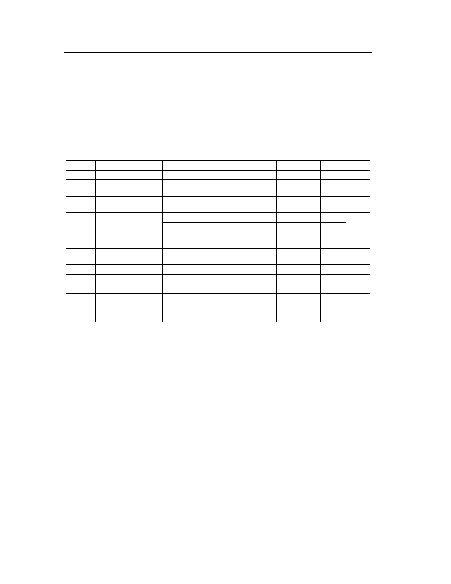
DC Electrical Characteristics
over recommended operating conditions unless specified otherwise All typical values are measured at V
CC
e
5V T
A
e
25 C
Symbol
Parameter
Conditions
Min
Typ
Max
Units
V
IK
Input Clamp Voltage
V
CC
e
4 5V I
I
e b
18 mA
b
1 2
V
V
IH
Minimum Input
2 0
V
High Level Voltage
V
IL
Maximum Input
0 8
V
Low Level Voltage
V
OH
High Level Output
I
OH
e b
3 mA V
CC
e
4 5V
2 4
Voltage
I
OH
e b
48 mA V
CC
e
4 5V
2 0
V
V
OL
Low Level Output
V
CC
e
4 5V I
OL
e
64 mA
0 35
0 5
V
Voltage
I
I
Input Current
V
CC
e
5 5V V
IH
e
7V
0 1
mA
Max Input Voltage
I
IH
High Level Input Current
V
CC
e
5 5V V
IH
e
2 7V
20
m
A
I
IL
Low Level Input Current
V
CC
e
5 5V V
IH
e
0 4V
b
0 5
mA
I
O
Output Drive Current
V
CC
e
5 5V V
O
e
2 25V
b
50
b
150
mA
I
CC
Supply Current
V
CC
e
5 5V
Outputs High
8
15
mA
Outputs Low
32
42
mA
C
IN
Input Capacitance
V
CC
e
5V
5
pF
3
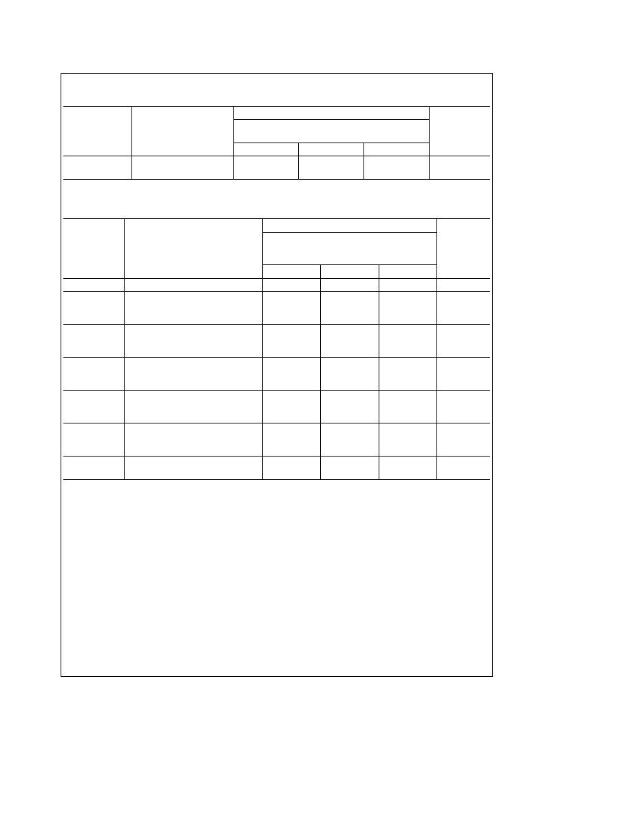
AC Electrical Characteristics
Over recommended operating conditions unless specified otherwise
CGS74B2525
Symbol
Parameter
V
CC
e
4 5V to 5 5V
Units
R
L
e
500X C
L
e
50 pF
Min
Typ
Max
t
PLH
Propagation Delay
2
3 0
4 8
ns
t
PHL
CLK to O
n
2
3 0
4 8
Extended AC Electrical Characteristics
Over recommended operating conditions unless specified otherwise
Symbol
Parameter
CGS74B2525
Units
V
CC
e
4 5V to 5 5V
R
L
e
500X C
L
e
50 pF
T
A
e
0 C to 70 C
Min
Typ
Max
f
max
Maximum Operating Frequency
50
MHz
t
OSHL
Maximum Skew Common Edge
Output-to-Output Variation
150
600
ps
(Note 2)
t
OSLH
Maximum Skew Common Edge
Output-to-Output Variation
150
600
ps
(Note 2)
t
OST
Maximum Skew Opposite Edge
Output-to-Output Variation
0 7
1 5
ns
(Note 2)
t
PV
Maximum Skew
Part-to-Part Variation Skew
1 75
ns
(Note 3)
t
PS
Maximum Skew
Pin (Signal) Transition Variation
0 6
1 5
ns
(Note 2)
t
rise
Maximum Rise Fall Time
1 6
ns
t
fall
(from 0 8V to 2 0V 2 0V to 0 8V)
1 4
ns
Note 2
Output-to-Output Skew is defined as the absolute value of the difference between the actual propagation delay for any outputs within the same packaged
device The specifications apply to any outputs switching in the same direction either HIGH to LOW (t
OSHL
) or LOW to HIGH (t
OSLH
) or in opposite directions both
HL and LH (t
OST
) Parameters t
OST
and t
PS
guaranteed by design t
OSHL
and t
OSLH
are characterized and guaranteed by design
1 MHz
Note 3
Part-to-part skew is defined as the absolute value of the difference between the propagation delay for any outputs from device to device The parameter is
specified for a given set of conditions (i e capacitive load V
CC
temperature
of outputs switching etc ) Parameter guaranteed by design
Note 4
Load capacitance includes the test jig
4
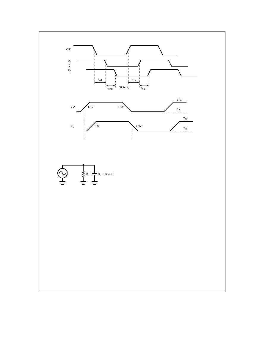
Timing Diagrams
TL F 10907 ≠ 16
TL F 10907 ≠ 17
Test Circuit
TL F 10907 ≠ 18
R
L
is 500X
C
L
is 50 pF for all prop delays and skew measurements
5