CGS74LCT2524
1 to 4 Minimum Skew (300 ps) 3V Clock Driver
General Description
This minimum skew clock driver is a 3V option of the current
CGS74CT2524 Minimum Skew Clock Driver and is designed
for Clock Generation and Support (CGS) applications oper-
ating at low voltage, high frequencies. This device guaran-
tees minimum output skew across the outputs of a given
device.
Skew parameters are also provided as a means to measure
duty cycle requirements as those found in high speed clock-
ing systems. This minimum skew clock driver with one input
driving four outputs, is specifically designed for signal gen-
eration and clock distribution applications.
Features
n
Ideal for low power/low noise high speed applications
n
Guaranteed:
-- 300 ps pin-to-pin skew (t
OSHL
and t
OSLH
)
n
Implemented on National's FACT
TM
family process
n
1 input to 4 outputs low skew clock distribution
n
Symmetric output current drive: 12 mA I
OH
/I
OL
n
Industrial temperature of -40∞C to +85∞C
n
8-pin SOIC package
n
Low dynamic power consumption above 20 MHz
n
Guaranteed 2 kV ESD protection
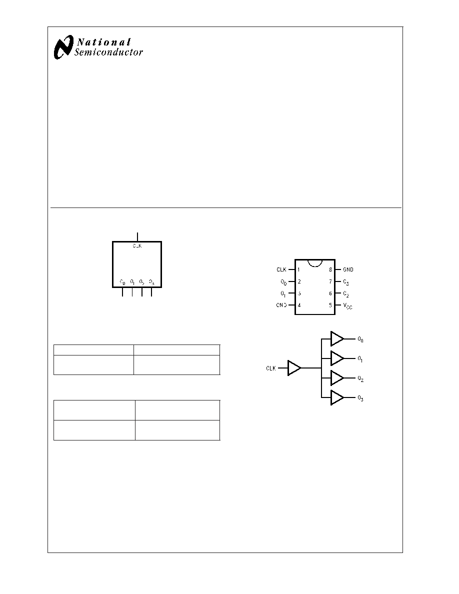
Logic Symbol
01195601
The output pins act as a single entity and will follow the state of the CLK
when the clock distribution chip is selected.
Pin Description
Pin Names
Description
CLK
Clock Input
O
0
≠O
3
Outputs
Truth Table
Inputs
Outputs
CLK
O
0
≠O
3
L
L
H
H
L = Low Logic Level
H = High Logic Level
Connection Diagrams
Pin Assignment
SOIC (MO)
01195602
01195603
See NS Package Number M08A
FACT
TM
is a trademark of National Semiconductor Corporation.
November 2003
CGS74LCT2524
1
t
o
4
Minimum
Skew
(300
ps)
3V
Clock
Driver
© 2003 National Semiconductor Corporation
DS011956
www.national.com
Absolute Maximum Ratings
(Note 1)
If Military/Aerospace specified devices are required,
please contact the National Semiconductor Sales Office/
Distributors for availability and specifications.
Supply Voltage (V
CC
)
-0.5V to 7.0V
DC Input Voltage Diode Current (I
IK
)
V = -0.5V
-20 mA
V = V
CC
+ 0.5V
+20 mA
DC Input Voltage (V
I
)
-0.5V to V
CC
+0.5V
DC Output Diode Current (I
O
)
V = -0.5V
-20 mA
V = V
CC
+ 0.5V
+20 mA
DC Output Voltage (V
O
)
-0.5V to V
CC
+0.5V
DC Output Source or Sink Current
(I
O
)
±
50 mA
DC V
CC
or Ground Current
per Output Pin (I
CC
or I
GND
)
±
50 mA
Storage Temperature (T
STG
)
-65∞C to +150∞C
Junction Temperature (
JA
)
Airflow
0 225
500 LFM
M 167 132 117 ∞C/W
Recommended Operating
Conditions
Supply Voltage (V
CC
)
3.0V to 3.6V
Input Voltage (V
IN
)
0V to V
CC
Output Voltage (V
O
)
0V to V
CC
Operating Temperature (T
A
)
Industrial
-40∞C to +85∞C
Commercial
0∞C to +70∞C
Input Rise and Fall Times
9.6 ns max
(0.8V to 2.0V)
Note 1: The Absolute Maximum Ratings are those values beyond which the
safety of the device cannot be guaranteed. The device should not be oper-
ated at these limits. The parametric values defined in the DC and AC
Electrical Characteristics tables are not guaranteed at the absolute maximum
ratings. The Recommended Operating Conditions will define the conditions
for actual device operation.
DC Electrical Characteristics
Over recommended operating conditions unless specified otherwise.
Symbol
Parameter
Conditions
V
CC
(V)
CGS74LCT2524
Units
T
A
= +25∞C
T
A
= -40∞C to +85∞C
Typ
Guaranteed Limits
V
IH
Minimum High Level
V
OUT
= 0.1V or V
CC
-0.1V
3.6
1.5
2.0
2.0
V
Input Voltage
V
IL
Maximum Low Level
V
OUT
= 0.1V or V
CC
-0.1V
3.6
1.5
0.8
0.8
V
Input Voltage
V
OH
Minimum High Level
V
IN
= V
IL
or V
IH
, I
OUT
= -50 µA
3.0
2.9
2.9
V
Output Voltage
V
IN
= V
IL
or V
IH
, I
OH
= -12 mA
3.0
2.5
2.4
V
V
OL
Minimum Low Level
V
IN
= V
IL
or V
IH
, I
OUT
= 50 µA
3.0
0.1
0.1
V
Output Voltage
V
IN
= V
IL
or V
IH
, I
OL
= -12 mA
3.0
0.3
0.4
V
I
IN
Maximum Input
V
IN
= V
CC
, GND
3.6
±
0.1
±
1.0
µA
Leakage Current
I
CCT
Maximum I
CC
/Input
V
IN
= 3.0V
3.6
100
µA
I
OLD
Minimum Dynamic
V
OLD
= 0.8V (max)
3.6
36
mA
I
OHD
Output Current
V
OHD
= 2.0V (min)
3.6
-25
mA
I
CC
Maximum Quiescent
V
IN
= V
CC
or GND
3.6
2.5
10
µA
Supply Current
CGS74LCT2524
www.national.com
2
AC Electrical Characteristics
Over recommended operating conditions unless specified otherwise. All typical values are measured at V
CC
= 3.3V, T
A
= 25∞C
Symbol
Parameter
LCT2524
Units
V
CC
= 3.0V to 3.6V
T
A
= -40∞C to +85∞C
C
L
= 50 pF
R
L
= 500
Min
Typ
Max
t
PLH
Low-to-High Propagation Delay
6
15.0
ns
CLK to O
n
t
PHL
High-to-Low Propagation Delay
6
15.0
ns
CLK to O
n
Extended AC Electrical Characteristics
Over recommended operating conditions unless specified otherwise. All typical values are measured at V
CC
= 3.3V, T
A
= 25∞C
Symbol
Parameter
LCT2524
Units
V
CC
= 3.0V to 3.6V
T
A
= -40∞C to +85∞C
C
L
= 50 pF
R
L
= 500
Min
Typ
Max
f
max
Maximum Operating Frequency
75
MHz
t
OSHL
Maximum Skew Common Edge
300
ps
Output-to-Output Variation (Note 2)
t
OSLH
Maximum Skew Common Edge
300
ps
Output-to-Output Variation (Note 2)
t
PS
Maximum Skew
2.5
ns
Pin (Signal) Transition Variation (Note 3)
t
RISE
Rise Time/Fall Time
2.5
ns
t
FALL
(from 0.8V to 2.0V/2.0V to 0.8V)
T
HIGH
Time High
4
ns
T
LOW
Time Low
4
ns
Note 2: Output-to-Output Skew is defined as the absolute value of the difference between the actual propagation delay for any outputs within the same packaged
device. The specifications apply to any outputs switching in the same direction either HIGH-to-LOW (t
OSHL
) or LOW-to-HIGH (t
OSLH
) or in opposite directions both
HL and LH (t
OST
). Limits are characterized and guaranteed by design @ 66 MHz.
Note 3: Pin transition skew is the absolute difference between HIGH-to-LOW and LOW-to-HIGH propagation delay, measured at a given output pin.
Note 4: Refer to Minimum Skew Parameters Measurement Information Chart for definitions of each skew specification.
Note 5: Load capacitance includes the test jig.
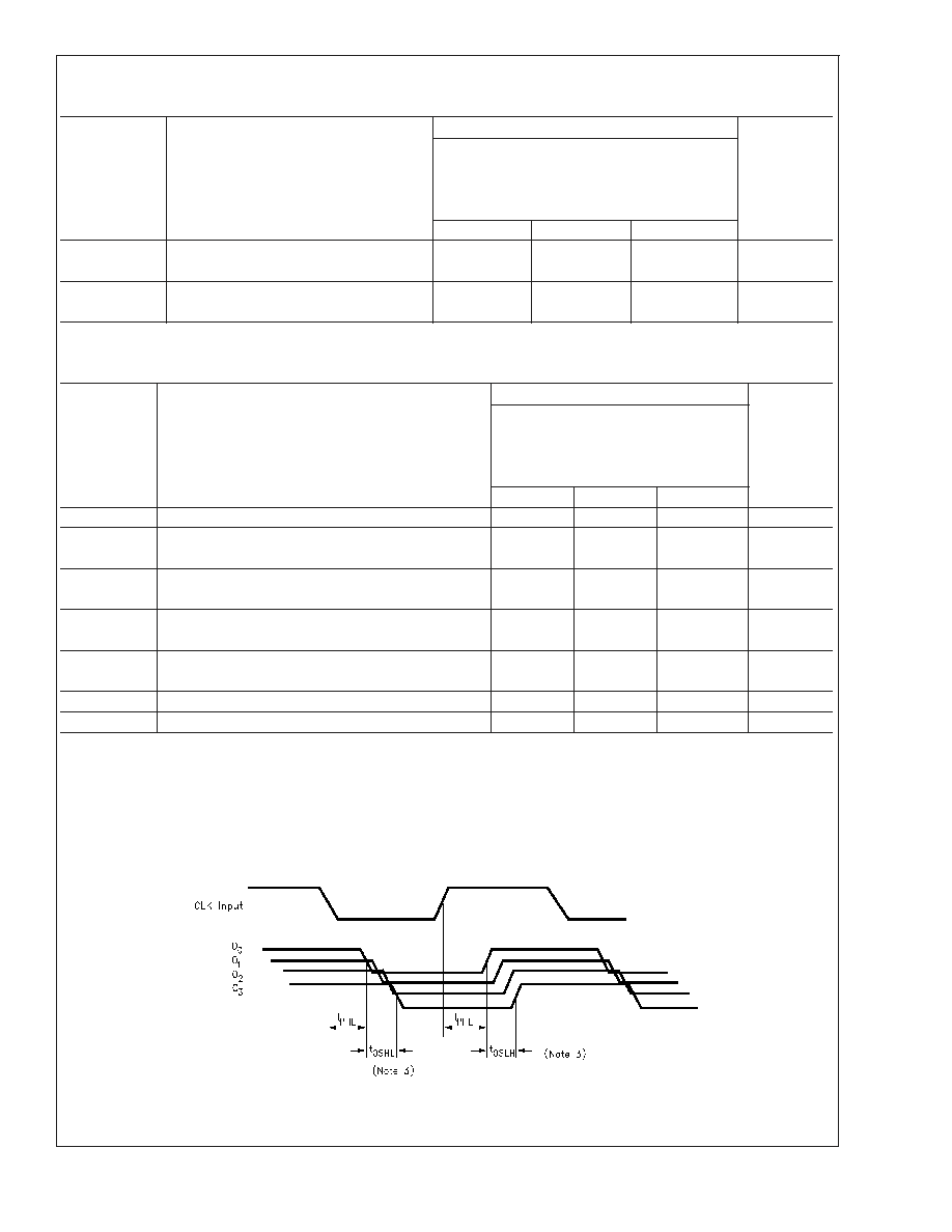
Timing Diagrams
01195605
CGS74LCT2524
www.national.com
3
Timing Diagrams
(Continued)
01195606
01195604
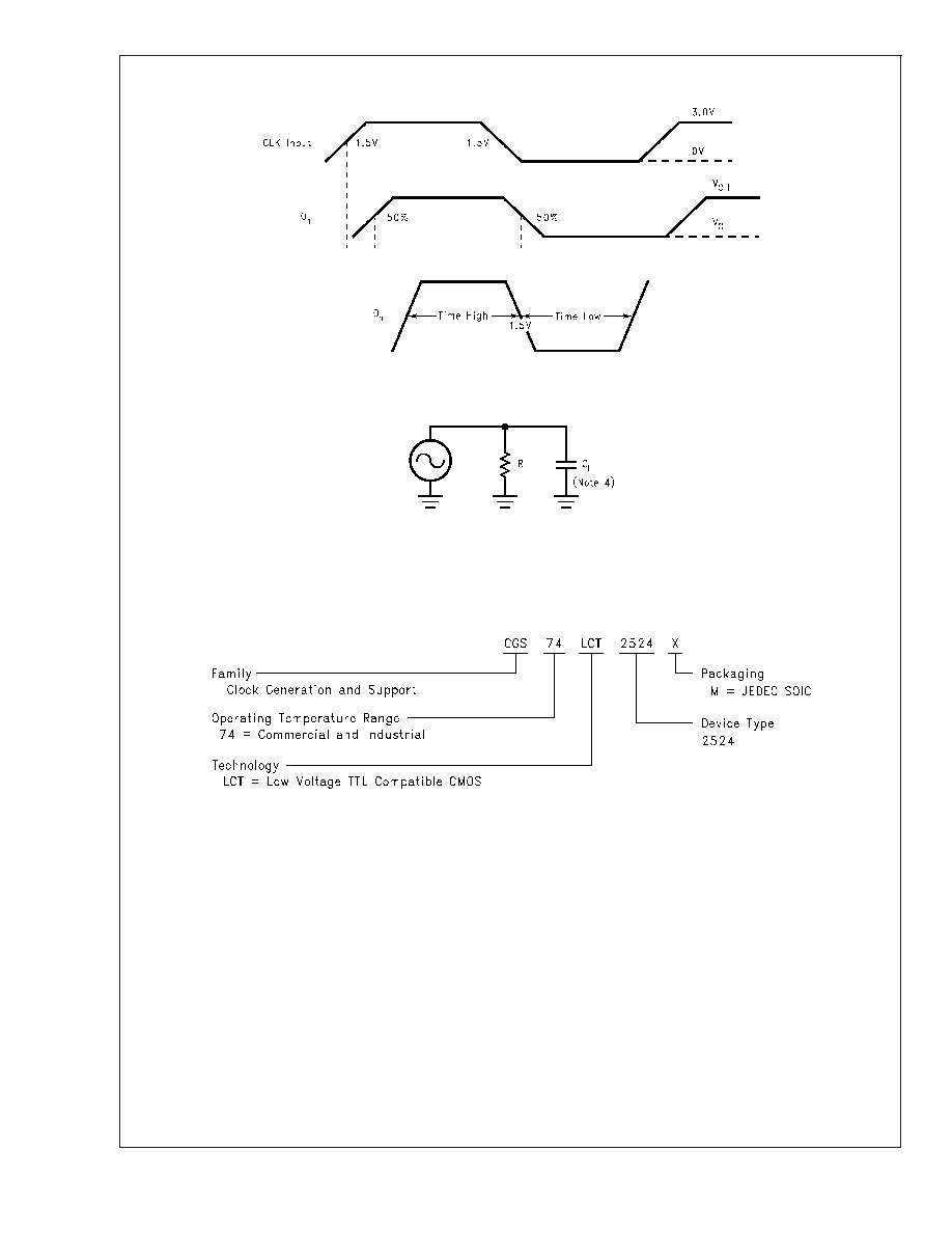
Test Circuit
01195607
R
L
is 500
C
L
is 50 pF for all propagation delays and skew measurements.
Ordering Information
(Contact NSC Mar-
keting for specific date of availability)
01195608
CGS74LCT2524
www.national.com
4
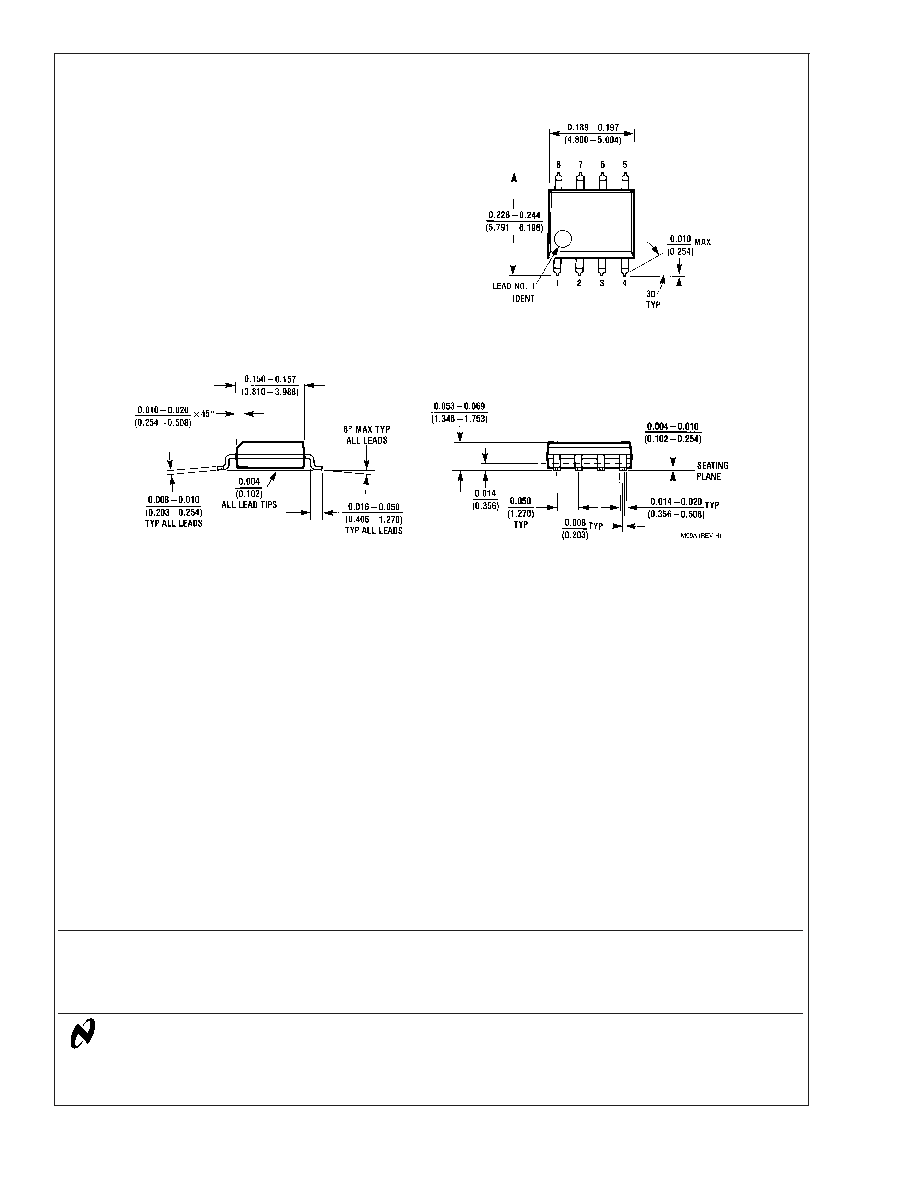
Physical Dimensions
inches (millimeters)
unless otherwise noted
8-Lead (0.150" Wide) Molded Small Outline Package, JEDEC
Order Number CGS74LCT2524M
NS Package Number M08A
LIFE SUPPORT POLICY
NATIONAL'S PRODUCTS ARE NOT AUTHORIZED FOR USE AS CRITICAL COMPONENTS IN LIFE SUPPORT
DEVICES OR SYSTEMS WITHOUT THE EXPRESS WRITTEN APPROVAL OF THE PRESIDENT AND GENERAL
COUNSEL OF NATIONAL SEMICONDUCTOR CORPORATION. As used herein:
1. Life support devices or systems are devices or
systems which, (a) are intended for surgical implant
into the body, or (b) support or sustain life, and
whose failure to perform when properly used in
accordance with instructions for use provided in the
labeling, can be reasonably expected to result in a
significant injury to the user.
2. A critical component is any component of a life
support device or system whose failure to perform
can be reasonably expected to cause the failure of
the life support device or system, or to affect its
safety or effectiveness.
BANNED SUBSTANCE COMPLIANCE
National Semiconductor certifies that the products and packing materials meet the provisions of the Customer Products
Stewardship Specification (CSP-9-111C2) and the Banned Substances and Materials of Interest Specification
(CSP-9-111S2) and contain no ``Banned Substances'' as defined in CSP-9-111S2.
National Semiconductor
Americas Customer
Support Center
Email: new.feedback@nsc.com
Tel: 1-800-272-9959
National Semiconductor
Europe Customer Support Center
Fax: +49 (0) 180-530 85 86
Email: europe.support@nsc.com
Deutsch Tel: +49 (0) 69 9508 6208
English
Tel: +44 (0) 870 24 0 2171
FranÁais Tel: +33 (0) 1 41 91 8790
National Semiconductor
Asia Pacific Customer
Support Center
Email: ap.support@nsc.com
National Semiconductor
Japan Customer Support Center
Fax: 81-3-5639-7507
Email: jpn.feedback@nsc.com
Tel: 81-3-5639-7560
www.national.com
CGS74LCT2524
1
t
o
4
Minimum
Skew
(300
ps)
3V
Clock
Driver
National does not assume any responsibility for use of any circuitry described, no circuit patent licenses are implied and National reserves the right at any time without notice to change said circuitry and specifications.