CLC001
Serial Digital Cable Driver with Adjustable Outputs
General Description
The CLC001 is a monolithic, high-speed cable driver
designed for use in SMPTE 259M serial digital video and
ITU-T G.703 serial digital data transmission applications.
The CLC001 drives 75
transmission lines (Belden 8281 or
equivalent) at data rates up to 622 Mbps. Controlled output
rise and fall times (400 ps typical) minimize transition-
induced jitter. The output voltage swing is adjustable from
800 mV
p-p
to 1.0 V
p-p
using an external resistor.
The CLC001's output stage consumes less power than other
designs. The differential inputs accept LVDS signal levels,
LVPECL levels directly or PECL with attenuation networks.
All these make the CLC001 an excellent general purpose
high speed driver for high-speed, long distance data
transmission applications.
The CLC001 is powered from a single +3.3V supply and
comes in a small 8-pin SOIC package.
Key Specifications
n
400 ps rise and fall times
n
Data rates to 622 Mbps
n
100 mV differential input threshold
n
Low residual jitter
Features
n
Adjustable output amplitude
n
Differential input and output
n
Accepts LVPECL or LVDS input swings
n
Low power dissipation
n
Single +3.3V supply
Applications
n
Digital routers and distribution amplifiers
n
Coaxial cable driver for digital transmission lines
n
Twisted pair driver
n
Serial digital video interfaces for the commercial and
broadcast industry
n
SMPTE, Sonet/SDH, and ATM compatible driver
n
Buffer applications
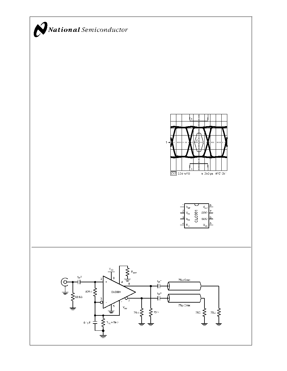
Connection Diagram (8-Pin SOIC)
Typical Application
DS101329-10
622 Mbps Eye Pattern with STM-4 Signal Mask
DS101329-2
Order Number CLC001AJE
See NS Package Number M08A
DS101329-1
March 2001
CLC001
Serial
Digital
Cable
Driver
with
Adjustable
Outputs
� 2001 National Semiconductor Corporation
DS101329
www.national.com
Absolute Maximum Ratings
(Note 1)
If Military/Aerospace specified devices are required,
please contact the National Semiconductor Sales
Office/Distributors for availability and specifications.
Supply Voltage
4V
Output Current
27 mA
Maximum Junction Temperature
+125�C
Storage Temperature Range
-65�C to +150�C
Lead Temperature
(Soldering 10 seconds)
+300�C
ESD Rating (HBM)
7 kV
ESD Rating (MM)
500V
Package Thermal Resistance
JA
Surface Mount AJE
125�C/W
JC
Surface Mount AJE
105�C/W
Reliability Information
Transistor count
291
Recommended Operating
Conditions
Supply Voltage Range (V
DD
- V
SS
)
+3.0V to +3.6V
Operating Free Air Temperature (T
A
)
-40�C to +85�C
R
BB
Range (applied to V
BB
input)
(Note 6)
1.3k
to 11.5k
Electrical Characteristics
Over recommended operating supply and temperature ranges unless otherwise specified (Notes 2 and 3)
Symbol
Parameter
Conditions
Min
Typ
Max
Units
OUTPUT DC SPECIFICATIONS
V
SDO
Serial Driver Output Voltage
R
L
= 75
1%,
R
REF
= 1.91 k
1% (for 800 mV
p-p
),
Figure 1
720
800
880
mV
R
L
= 75
1%,
R
REF
= 1.5 k
1% (for 1.0 V
p-p
),
Figure 1
900
1000
1100
mV
INPUT DC SPECIFICATIONS
V
TH
Differential Input High Threshold
V
CM
= +0.05V or +1.2V or +3.25V,
0
+100
mV
V
TL
Differential Input Low Threshold
V
DD
= 3.3V
-100
0
mV
V
CMR
Common Mode Voltage Range
V
ID
= 100mV, V
DD
= 3.3V
0.05
3.25
V
I
IN
Input Current
V
IN
= 0V or +3.0V, V
DD
= 3.6V or 0V
�
1
�
10
�A
I
INB
Input Current Balance
V
IN
= 0V or +3.0V, V
DD
= 3.6V or 0V,
(Note 8)
0.23
�A
SUPPLY CURRENT
I
DD
Total Dynamic Power Supply Current
(includes load current)
R
L
= 75
,
R
REF
= 1.91 k
1%
(V
SDO
= 800 mV
p-p
@
270 Mbps)
70
115
mA
R
L
= 75
,
R
REF
= 1.5 k
1%
(V
SDO
= 1.0 V
p-p
@
622 Mbps)
85
130
mA
MISCELLANEOUS PARAMETERS
L
GEN
Output Inductance
6
nH
R
GEN
Output Resistance
25
k
I
BB
V
BB
Current
R
REF
= 1.91 k
1%, (Note 6)
250
�A
R
REF
= 1.5 k
1%, (Note 6)
315
�A
CLC001
www.national.com
2
AC Electrical Characteristics
Over recommended operating supply and temperature ranges unless otherwise specified (Note 3)
Symbol
Parameter
Conditions
Min
Typ
Max
Units
t
r
, t
f
Rise time, Fall time
20%�80%, (Notes 4, 5)
400
800
ps
t
os
Output overshoot
5
%
t
jit
Output jitter
(Note 7)
25
ps
t
pd
Propagation delay
(Note 5)
1.9
ns
Note 1: "Absolute Maximum Ratings" are those values beyond which the safety of the device cannot be guaranteed. They are not meant to imply that the devices
should be operated at these limits. The table of "Electrical Characteristics" specifies conditions of device operation.
Note 2: Current flow into device pins is defined as positive. Current flow out of device pins is defined as negative. All voltages are stated referenced to V
SS
= 0V.
Note 3: Typical values are at 25�C and 3.3V.
Note 4: This parameter is Guaranteed by Design.
Note 5: R
L
= 75
, AC-coupled at 270 Mbps, R
REF
= 1.91 k
1% (for V
SDO
= 800 mV
p-p
�
10%), C
L
not greater than 5pF (See
Figure 1
)
Note 6: The V
BB
output is intended as a bias supply pin for the inputs of this device only. It is not designed as a power supply output and should not be used to
power other devices.
Note 7: R
L
= 75
, AC-coupled at 622 Mbps, R
REF
= 1.5 k
1% (for V
SDO
= 1.0 V
p-p
�
10%), clock pattern input.
Note 8: Input Current Balance (I
INB
) is the difference between the Input Current (I
IN
) on V
IN+
and V
IN-
for the same bias condition.
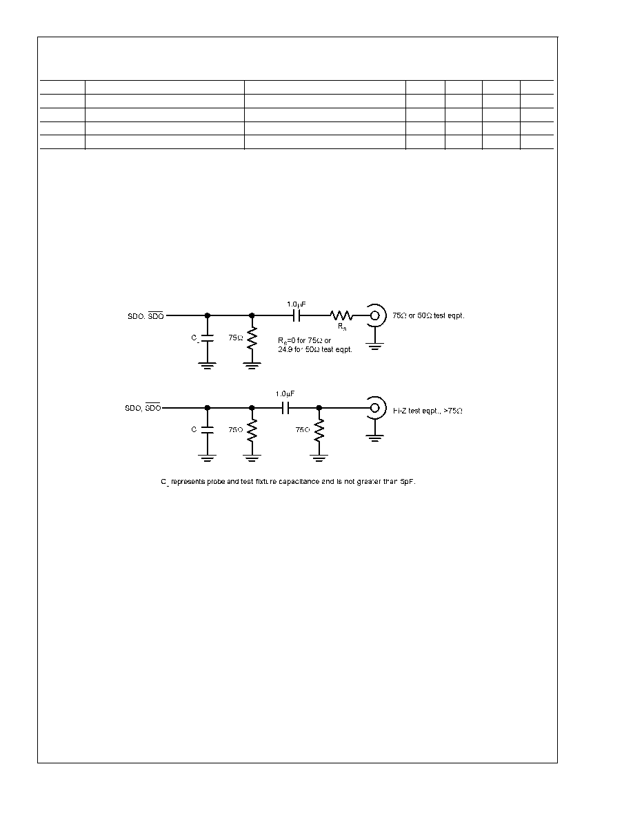
Test Loads
DS101329-4
FIGURE 1. Test Loads
CLC001
www.national.com
3
Test Loads
(Continued)
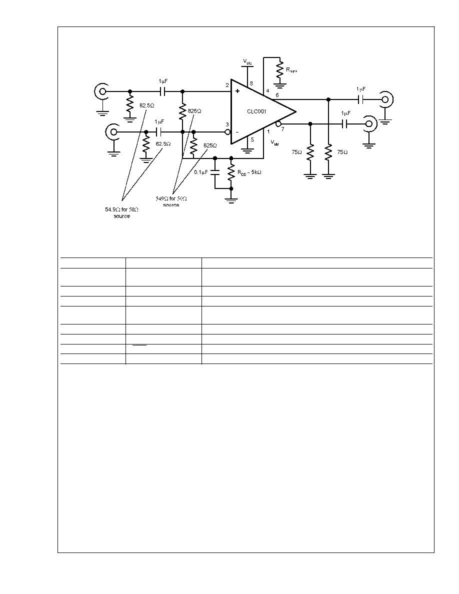
Pin Descriptions
Pin #
Name
Description
1
V
BB
Optional, bias voltage (may be used to bias inputs) - see device operation
section for details. If unused leave as no connect (NC).
2
V
IN+
Positive input pin
3
V
IN-
Negative input pin
4
R
REF
Output driver level control. Connect a resistor to ground to set output voltage
swing.
5
V
SS
Negative power supply
6
SDO
Serial data true output
7
SDO
Serial data complement output
8
V
DD
Positive power supply
DS101329-3
FIGURE 2. Test Circuit
CLC001
www.national.com
4
Device Operation
INPUT INTERFACING
Numerous input configurations exist for applying PECL,
LVPECL, and LVDS signals to the input of the CLC001.
Inputs may be single-ended or differential, AC or DC
coupled.
The V
BB
pin may be used to provide a DC bias voltage to
the inputs. Leave this pin as a no connect when no bias is
needed. Note that DC-coupled inputs such as direct
LVDS and LVPECL connections are self-biasing and do
not require use of the V
BB
pin. I
BB
, the current produced
by the V
BB
pin, depends on R
REF
. For a given R
REF
, the
I
BB
current will remain constant, and the bias voltage is
determined by the value of resistance, R
BB
, between the
V
BB
pin and ground.
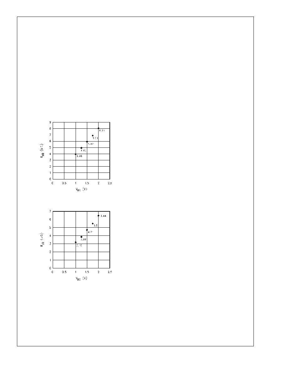
Figure 3 and Figure 4 show how R
BB
corresponds to some common V
BB
values with R
REF
held
at 1.91 k
and 1.5 k
, respectively. Some common input
configurations are shown in
Figure 5 through Figure 9.
DS101329-11
FIGURE 3. R
BB
vs. V
BB
for R
REF
= 1.91 k
DS101329-12
FIGURE 4. R
BB
vs. V
BB
for R
REF
= 1.5 k
CLC001
www.national.com
5