CLC011
Serial Digital Video Decoder
General Description
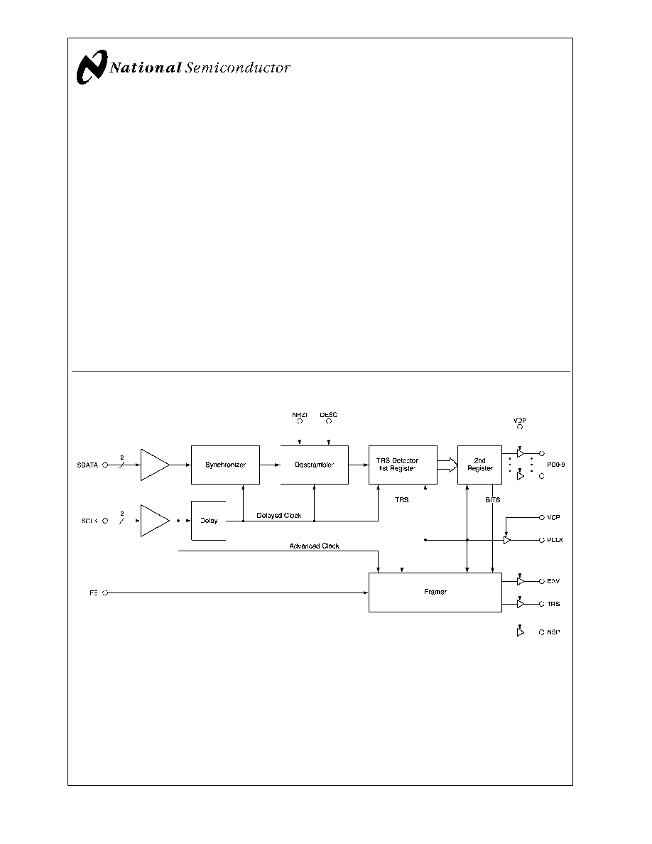
National's Comlinear CLC011, Serial Digital Video Decoder,
decodes and descrambles SMPTE 259M standard Serial
Digital Video datastreams with serial clock into 10-bit parallel
words and a corresponding word-rate clock. SMPTE 259M
standard parallel data is encoded and scrambled using a
9-bit shift register and is also converted from NRZ to NRZI.
The CLC011 restores the original parallel data by reversing
the encoding process. The CLC011 also extracts timing
information embedded in the SDV data. These reserved
code words, known as Timing Reference Signals (TRS),
indicate the start and end of each active video line. By
decoding the TRS, the CLC011 correctly identifies the word
boundaries of the encoded input data. Detection of the TRS
reserved codes is indicated by low-true signals at the TRS
and End of Active Video (EAV) outputs.
The CLC011's design using current-mode logic (CML) re-
duces noise injection into the power supply thereby easing
board layout and interfacing. The CMOS compatible outputs,
which feature controlled rise and fall times, may be set for
either 3.3V or 5V swings with the VDP and VCP inputs.
The CLC011 Serial Digital Video Decoder, CLC014 Adaptive
Cable Equalizer and the CLC016 Data Retiming PLL com-
bine to provide a complete Serial Digital Video receiver
system.
The CLC011 is packaged in a 28-pin PLCC.
Features
n
Data decoding and deserializing
n
CLC011B operates to 360Mbps
n
Low noise injection to power supplies
n
Single +5V or -5.2V supply operation
n
Output levels programmable for interface to 5V or 3.3V
logic
n
Low power
n
Low cost
Block Diagram
10008601
July 2002
CLC01
1
Serial
Digital
V
ideo
Decoder
© 2002 National Semiconductor Corporation
DS100086
www.national.com
Connection Diagram
10008602
28-Pin PLCC
Order Number CLC011BCQ
See NS Package Number V28A
Pin Descriptions
Name
Pin No.
Description
EAV
1
End of active video flag. For component video, a logic low is output for one cycle of the parallel
clock every time an EAV timing reference is detected. The pulse is aligned with the fourth word
of the timing reference (the XYZ word). For composite video, this line is always asserted high.
V
EE
2, 4, 26
Negative supply pins.
NC
3
Unused pin.
SDI+, SDI-
5, 6
Differential serial data inputs.
SCI+, SCI-
7, 8
Differential serial clock inputs.
NRZI
9
A logic high at this pin enables NRZI-to-NRZ conversion.
DESC
10
A logic high at this pin enables descrambling.
FE
11
Frame enable. Enables resynchronization of the parallel word at the next TRS.
V
CC
12
Positive supply pin.
VCP
13
Parallel clock high level programming pin. The voltage at this supply pin defines the logic high
level for the parallel clock output.
NSP
14
New sync position. Indicates that the most recent TRS is in a new position relative to the
previous TRS. Remains high until the parallel rate clock is aligned properly with the TRS.
TRS
15
Timing reference flag. A logic low is output for the duration of the TRS.
PCLK
16
Parallel clock output. The rising edge of this clock is located at the center of the parallel data
window.
PD0≠9
17,
19≠25,
27, 28
Parallel data outputs.
VDP
18
Parallel data high level programming pin. The voltage at this supply pin defines the logic high
level for the data outputs.
CLC01
1
www.national.com
2
Absolute Maximum Ratings
(Note 1)
If Military/Aerospace specified devices are required,
please contact the National Semiconductor Sales Office/
Distributors for availability and specifications.
Supply Voltage (V
CC
≠V
EE
)
+6V
Storage Temperature Range
-65∞C to +150∞C
Junction Temperature
+150∞C
ESD Rating (HBM)
PDx
500V
other
2kV
Package Thermal Resistance
JA
28-Pin PLCC
85∞C/W
JC
28-Pin PLCC
35∞C/W
Reliability Information
Transistor Count
3076
Recommended Operating
Conditions
Supply Voltage (V
CC
≠V
EE
)
4.5V to 5.5V
Logic High Voltage
(V
CP
≠V
EE
and V
DP
≠V
EE
)
3.0V to 5.5V
Operating Temperature
0∞C to +70∞C
Electrical Characteristics
(V
CC
= +5V, V
EE
= 0V, C
L
= 10 pF; unless specified).
Parameter
Conditions
Typ
+25∞C
Min/Max
+25∞C
Min/Max
0∞C to
+70∞C
Units
DYNAMIC PERFORMANCE
Minimum Serial Data Rate
0
Mbps
Maximum Serial Data Rate
400
360
360
Mbps
PDn and PCLK Rise/Fall Time
C
L
= 2 pF,(Note 9)
2.0
ns
PDn and PCLK Rise/Fall Time
C
L
= 20 pF,(Note 9)
4.0
ns
PCLK Rising Edge Residual Jitter
(Note 9)
50
ps
pp
TIMING PERFORMANCE
SD to SC Setup Time
0.2
0.2
ns
SC to SD Hold Time
0
0
ns
PDn to PCLK Skew
(Note 9)
±
0.8
ns
PDn Valid to PCLK
PCLK = 27 MHz, (Note 9)
18
ns
PCLK
to PDn Invalid
PCLK = 27 MHz, (Note 9)
18
ns
Digital Latency
(Notes 6, 7, 9)
42
sclk cycles
Output Buffer Latency
(Notes 7, 9)
10
ns
STATIC PERFORMANCE
I
CC
Supply Current
(Note 9) V
CC
Pin
44
mA
VDP and VCP Supply Current
PCLK = 0 MHz, (Note 9)
2
mA
VDP and VCP Supply Current
PCLK = 27 MHz, (Note 9)
12
mA
SD and SC Inputs
Input Range Upper Limit
V
CC
V
CC
V
Input Range Lower Limit
V
EE
+2.5
V
EE
+2.5
V
Minimum Differential Input
200
200
mV
I
IH
10
15
µA
FE, NRZI, and DESC Inputs
V
IL
V
EE
+0.8
V
EE
+0.8
V
V
IH
V
EE
+2.0
V
EE
+2.0
V
Outputs
V
OL
I
OL
= 10 mA
V
EE
+0.5
V
EE
+0.5
V
V
OH
I
OH
= 10 mA
V
CC
-0.5
V
CC
-0.5
V
MISCELLANEOUS PERFORMANCE
SD and SC Input Capacitance
(Note 9)
2.0
pF
SD and SC Input Resistance
(Note 9)
20
k
Note 1: "Absolute Maximum Ratings" are those values beyond which the safety of the device cannot be guaranteed. They are not meant to imply that the devices
should be operated at these limits. The table of "Electrical Characteristics" specifies conditions of device operation.
CLC01
1
www.national.com
3
Electrical Characteristics
(Continued)
Note 2: Min/Max ratings are based on product characterization and simulation. Individual parameters are tested as noted. Outgoing quality levels are determined
from tested parameters.
Note 3: Nominal position of rising edge of serial clock is at the center of the serial data eye.
Note 4: Nominal position of the rising edge of PCLK is at the center of the PDn eye.
Note 5: See Timing Diagrams.
Note 6: Data latency due to digital registers, measured from MSB of serial data to parallel clock out.
Note 7: Total latency is the digital latency plus the output buffer latency.
Note 8: 100% tested at 25∞C, sample tested over temperature.
Note 9: Typicals only specified.
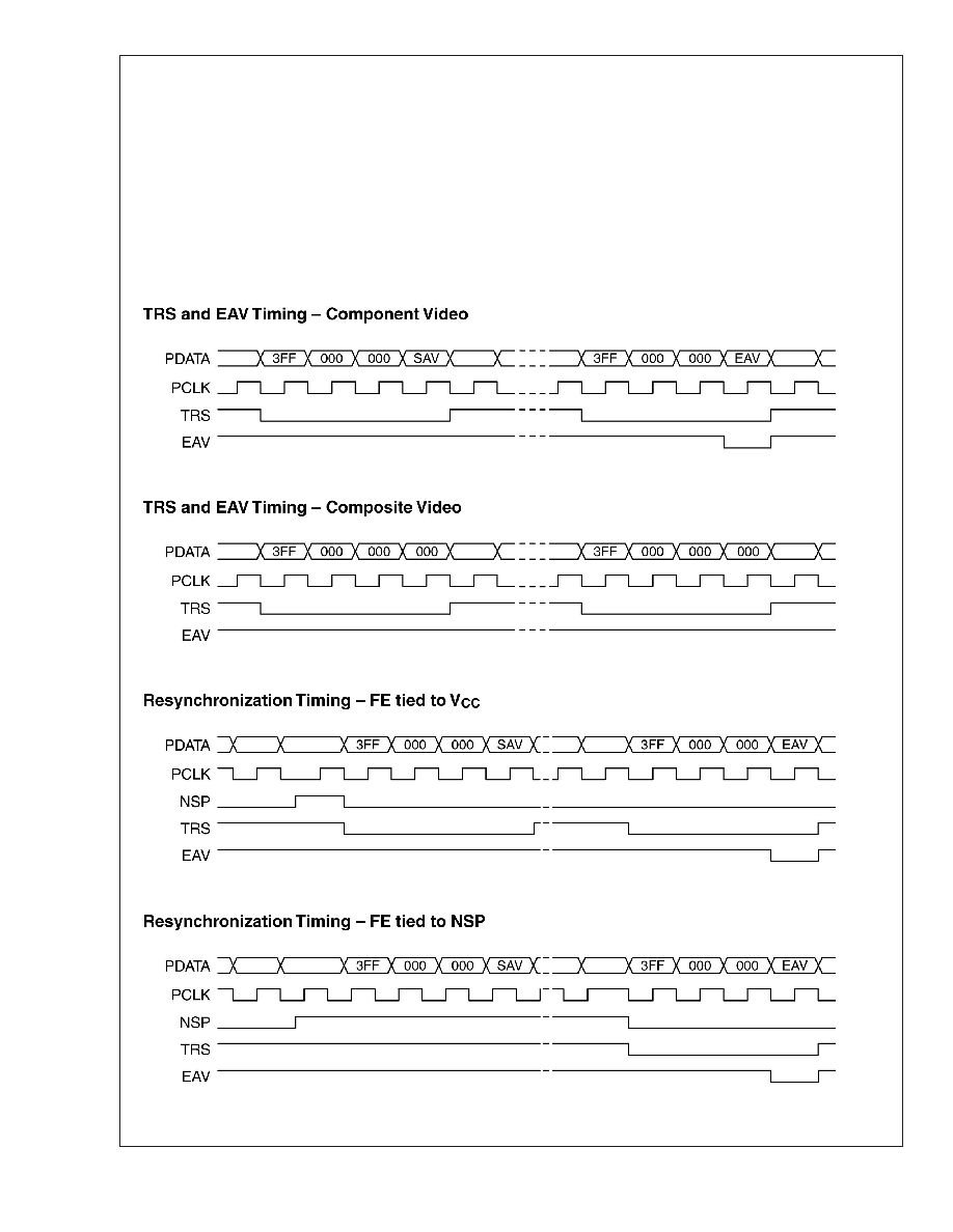
Timing Diagrams
10008603
FIGURE 1.
CLC01
1
www.national.com
4
Overview
The CLC011, Serial Digital Video Decoder, decodes and
descrambles SMPTE 259M standard Serial Digital Video
datastreams into 10-bit parallel words and a corresponding
word-rate clock. The following information describes:
∑
the CLC011 operation,
∑
recommended interface circuitry, and
∑
PCB layout suggestions.
Applications assistance for the CLC011 may be obtained by
calling the Interface Applications Hotline, (408) 721-8500.
Input Interfacing--Signal Inputs
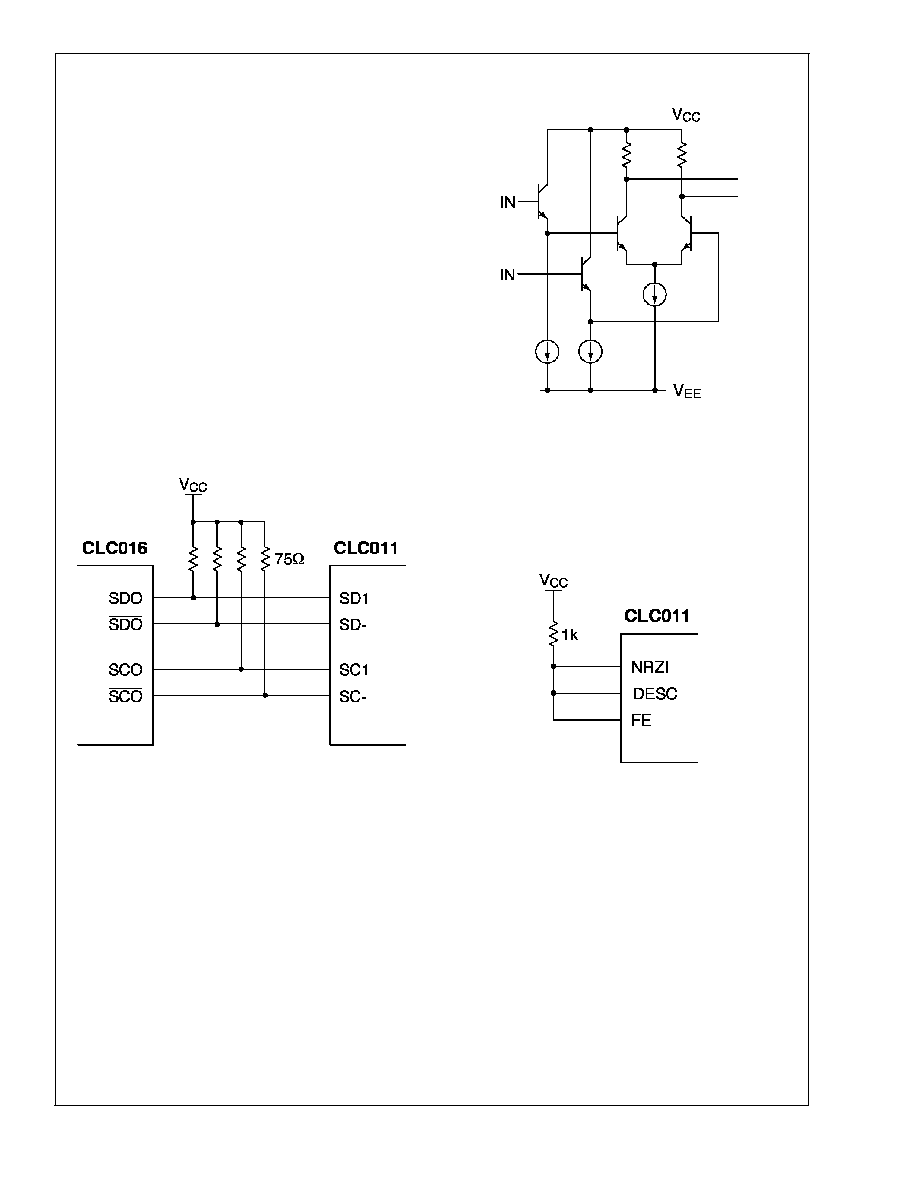
The serial data and clock inputs of the CLC011 are both
differential. Their input voltage ranges from 2.5V above the
negative supply (V
EE
+2.5V) to the positive supply voltage
(V
CC
). Supply voltages for the CLC011 may be either +5V or
≠5.2V for ECL compatibility and interfacing. When operated
from the negative supply, inputs accept standard ECL signal
levels. The minimum differential input swing is 200 mV. The
CLC011 interfaces with the CLC016 Data Retiming PLL as
shown in Figure 2. A simplified schematic of the CLC011's
signal inputs appears in Figure 3.
Input Interfacing--Control Inputs
Three TTL-compatible inputs control operation of the
CLC011: NRZI, DESC and FE. A typical interface circuit for
the control inputs is shown in Figure 4.
NRZI: NRZI, when a logic high, enables NRZI to NRZ con-
version. For standard SMPTE 259M operation, NRZI is high.
DESC
(Descramble): The
bits
of
a
SMPTE
259M
datastream are scrambled upon encoding according to a
polynomial equation. DESC, when a logic high, enables
descrambling of the encoded signal. For standard SMPTE
259M operation, DESC is high.
FE (Framing Enable): SMPTE 259M datastreams include a
four-word-long reserved sequence known as the Timing Ref-
erence Signal (TRS). Using this sequence, the CLC011 de-
termines the position of word boundaries, also known as
framing, of the incoming data.
The FE input, when a logic high and following recognition of
a TRS, causes the CLC011 to automatically adjust its fram-
ing. The word boundary is aligned at the appropriate bit
position and the parallel output clock is aligned with the
appropriate cycle of the serial clock. When FE is held low
10008604
FIGURE 2. Interface with CLC016
10008605
FIGURE 3. Simplified Input Buffer Schematic
10008606
FIGURE 4. Typical Control Logic Connection
CLC01
1
www.national.com
5