CLC016
Data Retiming PLL with Automatic Rate Selection
General Description
National's Comlinear CLC016 is a low-cost, monolithic, data
retiming phase-locked loop (PLL) designed for high-speed
serial clock and data recovery. The CLC016 simplifies high-
speed data recovery in multi-rate systems by incorporating
auto-rate select (ARS) circuitry on chip. This function allows
the user to configure the CLC016 to recognize up to four
different data rates and automatically adjust to provide ac-
curate, low-jitter clock and data recovery. A single resistor is
used to set each data rate anywhere between 40 Mbps and
400 Mbps. No potentiometers, crystals, or other external ICs
are required to set the rate.
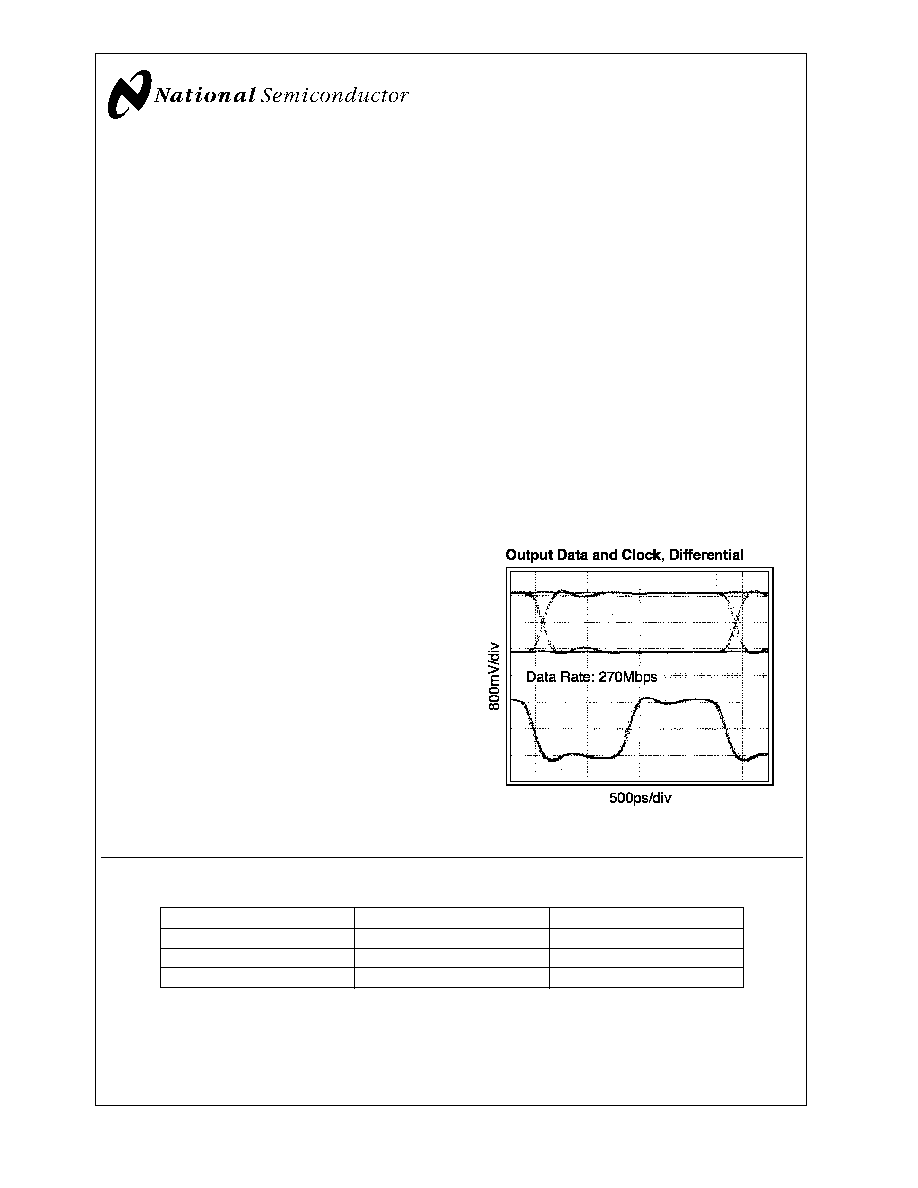
The CLC016 has output jitter of only 130 ps
pp
at a 270 Mbps
data rate and 0.25% fractional loop bandwidth. Low phase
detector output offset and low VCO injection combine to
ensure that the CLC016 does not generate bit errors or large
phase transients in response to extreme fluctuations in data
transition density. The result is improved performance when
handling the pathological patterns inherent in the SMPTE
259M video industry standard.
The carrier detect and output mute functions may be used
together to automatically latch the outputs when no data is
present, preventing random transitions. The external loop
filter allows the user to tailor the loop response to the specific
application needs. The CLC016 will operate with either +5V
or -5.2V power supplies. The serial data inputs and outputs,
as well as the recovered clock outputs, allow single- or
differential-ECL interfacing. The logic control inputs are TTL-
compatible.
Applications
n
SMPTE 259M serial digital interfaces: NTSC/PAL, 4:2:2
component, 360 Mbps wide screen
n
Serial digital video routing and distribution
n
Clock and data recovery for high-speed data
transmission
n
Re-synchronization of serial data for SONET/SDH, ATM,
CAD networks, medical and industrial imaging
Features
n
Retimed data output
n
Recovered clock output
n
Auto and manual rate select modes
n
Four user-configurable data rates
n
No potentiometers required
n
External loop bandwidth control
n
Frequency detector for lock acquisition
n
Carrier detect output
n
Output MUTE function
n
Single supply operation: +5V or -5.2V
n
Low cost
Key Specifications
n
Low jitter: 130 ps
pp
@
270 Mbps, 0.25% fractional loop
bandwidth (0.675 MHz)
n
High data rates: 40 Mbps - 400 Mbps
n
Low supply current: 100 mA, including output biasing
n
Flexible fractional loop bandwidth: from 0.05% to 0.5%
10008701
Ordering Information
Order Number
Temperature
Package
CLC016ACQ
0∞C to +70∞C
PLCC V28A
CLC016AJQ
≠40∞C to +85∞C
PLCC V28A
CLC016MTC
≠40∞C to +85∞C
TSSOP MTC28
July 2002
CLC016
Data
Retiming
PLL
with
Automatic
Rate
Selection
© 2002 National Semiconductor Corporation
DS100087
www.national.com
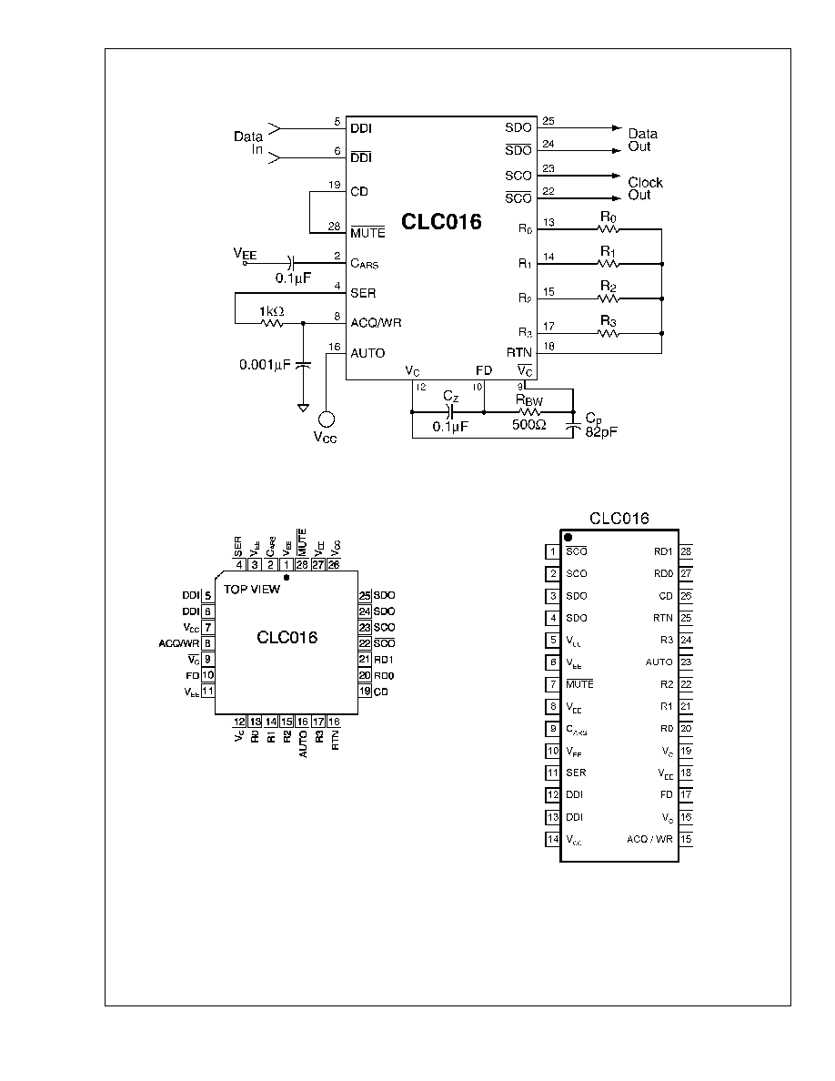
Typical Application
Four-Rate Clock and Data Recovery with Automatic Rate Selection - PLCC Package shown
10008702
Connection Diagrams
Pinout -Top View
10008703
28-pin PLCC
Pinout -Top View
10008757
28-pin TSSOP
CLC016
www.national.com
2
Absolute Maximum Ratings
(Note 1)
If Military/Aerospace specified devices are required,
please contact the National Semiconductor Sales Office/
Distributors for availability and specifications.
Supply Voltage (V
CC
≠V
EE
)
-0.3, +6.0V
Maximum Junction Temperature
+150∞C
Storage Temperature Range
-65∞C to +150∞C
Lead Temperature (Soldering 4 sec)
+260∞C
ESD Rating (Note 12)
2kV
Package Thermal Resistance
JA
28-Pin PLCC
85∞C/W
JA
28-Pin TSSOP
90∞C/W
JC
28-Pin PLCC
35∞C/W
JC
28-Pin TSSOP
14∞C/W
Reliability Information
MTTF (based on limited life
test data)
2.6 x 10
7
hours
Recommended Operating
Conditions
Supply Voltage (V
CC
≠V
EE
)
4.5V to 5.5V
Operating Temperature
CLC016AC
0∞C to +70∞C
CLC016AJ,CLC016
≠40∞C to +85∞C
Jitter Transfer Function Fractional
Loop Bandwidth
0.05% to 0.5%
SCO/SCO, SDO/ SDO Minimum
Voltage (Note 13)
V
CC
≠ 1.6V
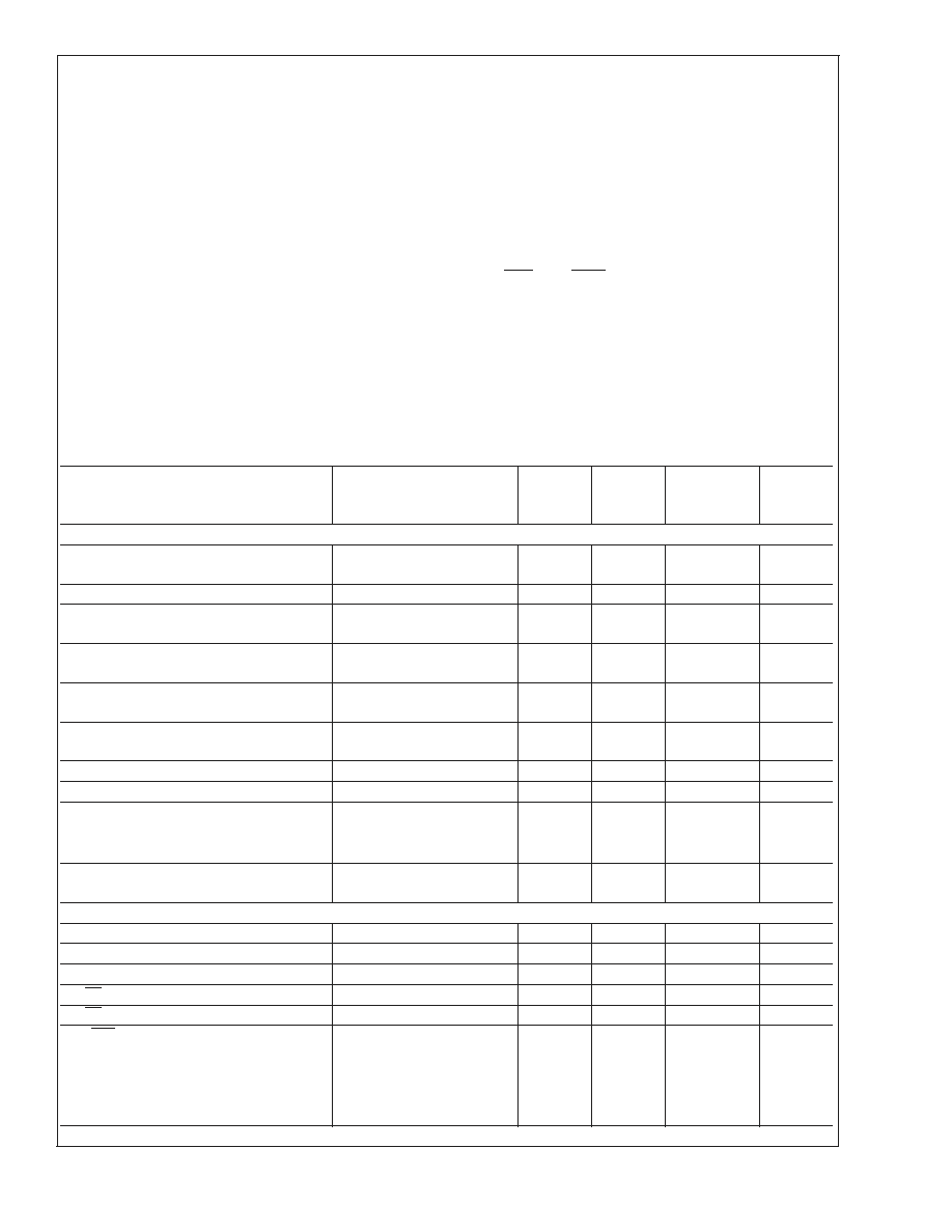
Electrical Characteristics
(V
CC
= 0V, V
EE
= -5V, R
BW
= 500
; C
Z
= 0.1 µF; C
P
= 82 pF; R
n
= 3504, C
ARS
= 0.1 µF; unless specified).
Parameter
Conditions
Typ
+25∞C
Min/Max
+25∞C
Min/Max
Full Temp.
Range
Units
DYNAMIC PERFORMANCE
Residual Jitter
270 Mbps PRN sequence
(Notes 3, 4)
150
250
300
ps
pp
Acquisition Time
270 Mbps PRN sequence
6 x 10
5
bit cells
Minimum Average Data Rate, f
CLK
Full Temperature Range
4.5V
(V
CC
- V
EE
)
5.5V
(Note 3)
100
Mbps
Minimum Average Data Rate, f
CLK
0 to 70∞
4.5V
(V
CC
- V
EE
)
5.5V
40
Mbps
Maximum Average Data Rate, f
CLK
4.5V
(V
CC
- V
EE
)
5.5V
(Note 3)
400
400
Mbps
Tracking and Capture Range
4.5V
(V
CC
- V
EE
)
5.5V
(Notes 3, 5)
±
8.3
±
5.0/
±
13.0
±
2.5/
±
18.0
%f
CLK
VCO Power Supply Sensitivity
(Note 3)
±
0.8
±
1.2
±
1.3
%V
VCO Temperature Sensitivity
±
250
ppm/∞C
Jitter Transfer Function -3 dB bandwidth
(Fractional Loop Bandwidth),
BW
R
BW
= 100
(Notes 6, 7)
0.05
%f
CLK
R
BW
= 500
(Notes 6, 7)
0.25
%f
CLK
R
BW
= 1000
(Notes 6, 7)
0.5
%f
CLK
Jitter Transfer Function Peaking
R
BW
= 500
, 270 Mbps
(Note 6)
<
0.1
dB
STATIC PERFORMANCE
Power Supply Current, I
EE
(Note 3)
105
125
133
mA
Voltage on Selected R
n
Resistor
(Note 8)
V
CC
-2.2
V
Voltage on Unselected R
n
Resistor
(Note 8)
V
CC
V
V
C
/V
C
Common-Mode Voltage, V
CM
(Note 8)
V
CC
-1.5
V
V
C
/V
C
Diff-Mode Voltage Range, V
DM
(Note 8)
±
300
mV
DDI/DDI
Input Range Upper Limit, V
H
V
CC
V
Input Range Lower Limit, V
L
V
EE
+2.5
V
Minimum Differential Input Amplitude, V
200
200
mV
Input Current
(Note 3)
3
6
6
µA
CLC016
www.national.com
3
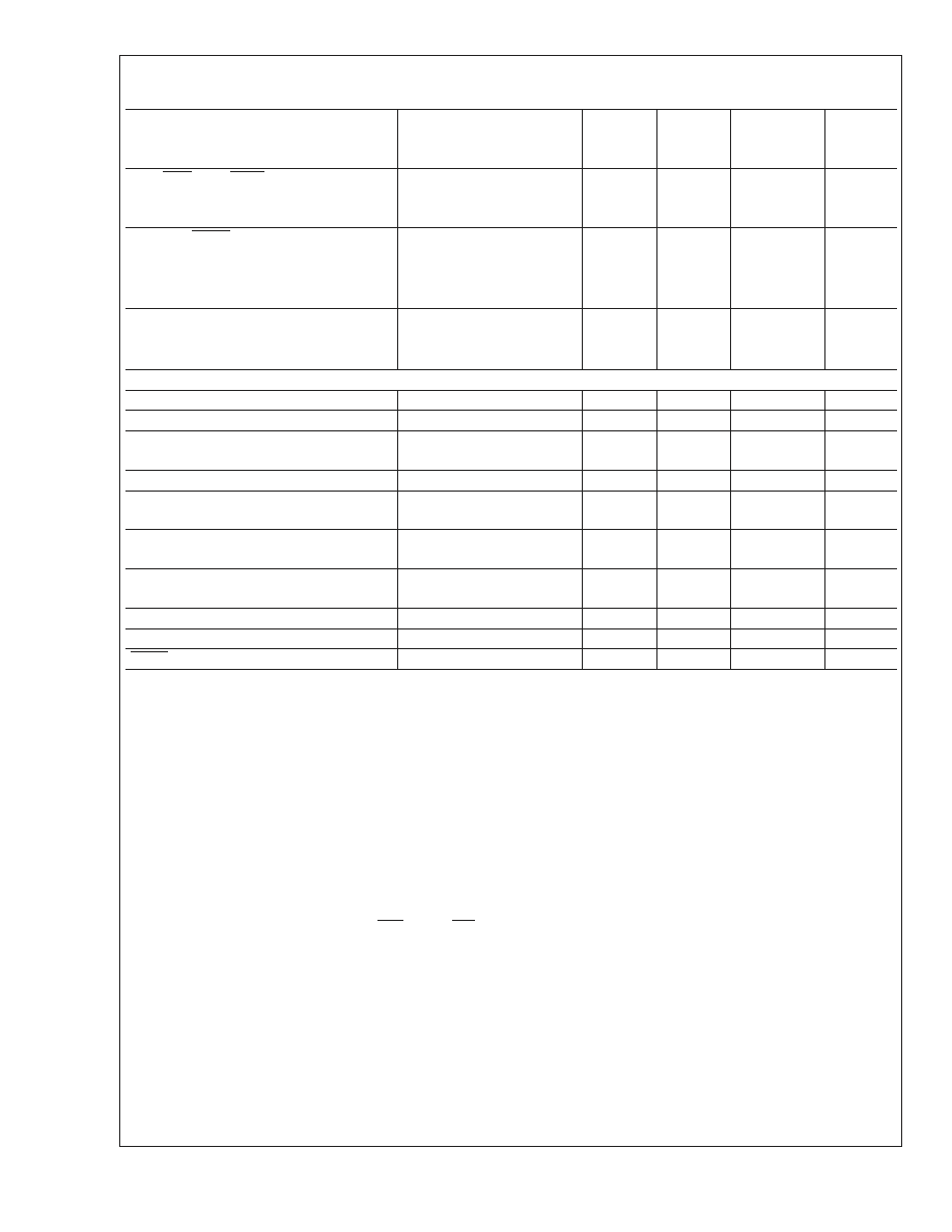
Electrical Characteristics
(Continued)
(V
CC
= 0V, V
EE
= -5V, R
BW
= 500
; C
Z
= 0.1 µF; C
P
= 82 pF; R
n
= 3504, C
ARS
= 0.1 µF; unless specified).
Parameter
Conditions
Typ
+25∞C
Min/Max
+25∞C
Min/Max
Full Temp.
Range
Units
SCO/SCO, SDO/ SDO
Output Current, I
OUT
(Note 3)
11
9.3/12
8.6/12.7
mA
Output Voltage Swing, V
OUT
R
collector
= 75
(Note 3)
725
625/900
mV
ACQ/WR, MUTE, RDO/RD1
Voltage Input -- LOW, V
IL
(Note 9)
V
EE
+ 0.8
V
EE
+ 0.8
V
Voltage Input -- HIGH, V
IH
(Note 3)
V
EE
+ 2.0
V
EE
+ 2.0
V
Input Current (I
IN
)
(Note 3)
±
100
±
500
nA
CD, UNL, RDO/RD1
(Note 9)
Current Output -- LOW, I
OL
V
OL
V
EE
+0.5V
800
µA
Current Output -- HIGH, I
OH
V
OH
V
CC
-0.5V
-700
µA
TIMING PERFORMANCE
Delay: SCO to SDO, t
d
200
ps
SCO Duty Cycle
(Note 3)
50
44/56
44/56
%
Rise/Fall Time: SCO, SDO, t
r
/t
f
20%≠80%, R
collector
= 75
(Note 10)
230
ps
SDO Duty Cycle Distortion
35
ps
Minimum Setup Time:
RDO/RD1 to ACQ/WR, t
SU
4
20
20
ns
Minimum Hold Time:
ACQ/WR to SS1/SS0, t
h
3
20
20
ns
Minimum Pulse Width:
ACQ/WR, t
w
5
20
20
ns
ARS Oscillator Period, t
OSC
(Note 3)
10.5
8.5/15.5
ms
CD Pulse Width, t
PW
(Note 11)
1
µs
MUTE Response Time, t
M
5
ns
Note 1: "Absolute Maximum Ratings" are those values beyond which the safety of the device cannot be guaranteed. They are not meant to imply that the devices
should be operated at these limits. The table of "Electrical Characteristics" specifies conditions of device operation.
Note 2: Min/Max ratings are based on product characterization and simulation. Individual parameters are tested as noted. Outgoing quality levels are determined
from tested parameters.
Note 3: J-level spec. is 100% tested at +25∞C.
Note 4: Peak-to-peak jitter is defined as 6 times the rms jitter.
Note 5: Tracking and capture range are specified as a percentage of the input data rate f
CLK
. The minimum and maximum are guaranteed so long as R
n
has been
chosen according to the equation in Resistor Selection for Data Rates.
Note 6: Average data transition density of 1 transition per 2 bit cells.
Note 7: When the value of R
BW
changes it is necessary to also change the values of C
P
and C
Z
. See Loop Filter Design.
Note 8: This information is provided for system troubleshooting purposes only.
Note 9: RD0/RD1 are inputs when AUTO = 0 and outputs when AUTO = 1.
Note 10: Includes typical pc board capacitance.
Note 11: The CD circuit is a retriggerable one-shot which retriggers on every data transition.
Note 12: Human body model, 1.5 k
in series with 100 pF.
Note 13: To maintain specified performance, SCO/ SCO and SDO/SDO should not drop below this level.
CLC016
www.national.com
4
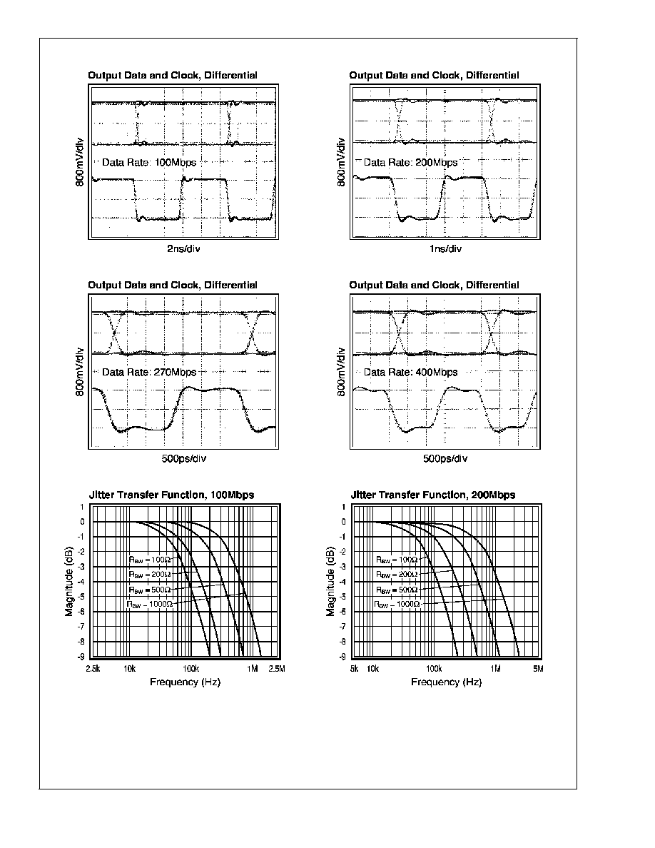
Typical Performance Characteristics
10008704
10008705
10008706
10008707
10008708
10008709
CLC016
www.national.com
5