CLC031
SMPTE 292M/259M Digital Video Deserializer /
Descrambler with Video and Ancilliary Data FIFOs
General Description
The
CLC031
SMPTE
292M
/
259M
Digital
Video
Deserializer/Descrambler with Video and Ancilliary Data
FIFOs is a monolithic integrated circuit that deserializes and
decodes SMPTE 292M, 1.485Gbps (or 1.483Gbps) serial
component video data, to 20-bit parallel data with a synchro-
nized parallel word-rate clock. It also deserializes and de-
codes
SMPTE
259M,
270Mbps,
360Mbps
and
SMPTE 344M (proposed) 540Mbps serial component video
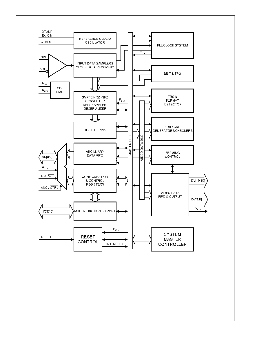
data, to 10-bit parallel data. Functions performed by the
CLC031 include: clock/data recovery from the serial data,
serial-to-parallel data conversion, SMPTE standard data de-
coding, NRZI-to-NRZ conversion, parallel data clock genera-
tion, word framing, CRC and EDH data checking and han-
dling, ancilliary data extraction and automatic video format
determination. The parallel video output features a variable-
depth FIFO which can be adjusted to delay the output data
up to 4 parallel data clock periods. Ancilliary data may be
selectively extracted from the parallel data through the use
of masking and control bits in the configuration and control
registers and stored in the on-chip FIFO. Reverse LSB dith-
ering is also implemented.
The unique multi-functional I/O port of the CLC031 provides
external access to functions and data stored in the configu-
ration and control registers. This feature allows the designer
greater flexibility in tailoring the CLC031 to the desired ap-
plication. The CLC031 is auto-configured to a default oper-
ating condition at power-on or after a reset command. Sepa-
rate power pins for the PLL, deserializer and other functional
circuits improve power supply rejection and noise perfor-
mance.
The CLC031 has a unique Built-In Self-Test (BIST) and
video Test Pattern Generator (TPG). The BIST enables com-
prehensive testing of the device by the user. The BIST uses
the TPG as input data and includes SD and HD component
video test patterns, reference black, PLL and EQ pathologi-
cals and a 75% saturation, 8 vertical colour bar pattern, for
all implemented rasters. The colour bar pattern has optional
transition coding at changes in the chroma and luma bar
data. The TPG data is output via the parallel data port.
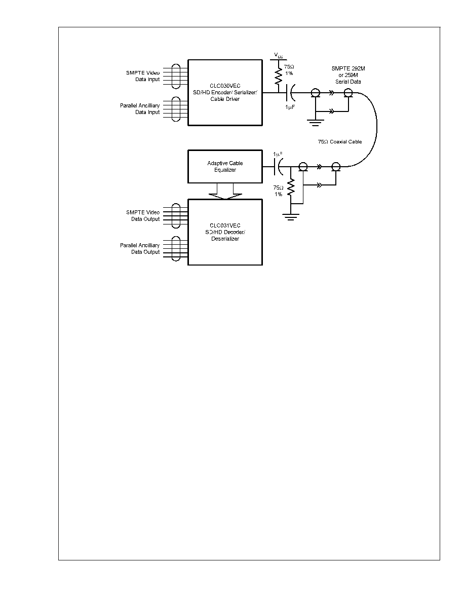
The CLC030, SMPTE 292M / 259M Digital Video Serializer
with Ancilliary Data FIFO and Integrated Cable Driver, is the
ideal complement to the CLC031.
The CLC031's internal circuitry is powered from +2.5 Volts
and the I/O circuitry from a +3.3 Volt supply. Power dissipa-
tion is typically 850mW. The device is packaged in a 64-pin
TQFP.
Features
n
SDTV/HDTV serial digital video standard compliant
n
Supports 270 Mbps, 360 Mbps, 540 Mbps, 1.483 Gbps
and 1.485 Gbps serial video data rates with
auto-detection
n
LSB de-dithering option
n
Uses low-cost 27MHz crystal or clock oscillator
reference
n
Fast VCO lock time:
<
500 µs at 1.485 Gbps
n
Built-in self-test (BIST) and video test pattern generator
(TPG)
*
n
Automatic EDH/CRC word and flag processing
n
Ancilliary data FIFO with extensive packet handling
options
n
Adjustable, 4-deep parallel output video data FIFO
n
Flexible control and configuration I/O port
n
LVCMOS compatible control inputs and clock and data
outputs
n
LVDS and ECL-compatible, differential, serial inputs
n
3.3V I/O power supply and 2.5V logic power supply
operation
n
Low power: typically 850mW
n
64-pin TQFP package
n
Commercial temperature range 0∞C to +70∞C
*
Patent applications made or pending.
Applications
n
SDTV/HDTV serial-to-parallel digital video interfaces for:
-- Video editing equipment
-- VTRs
-- Standards converters
-- Digital video routers and switchers
-- Digital video processing and editing equipment
-- Video test pattern generators and digital video test
equipment
-- Video signal generators
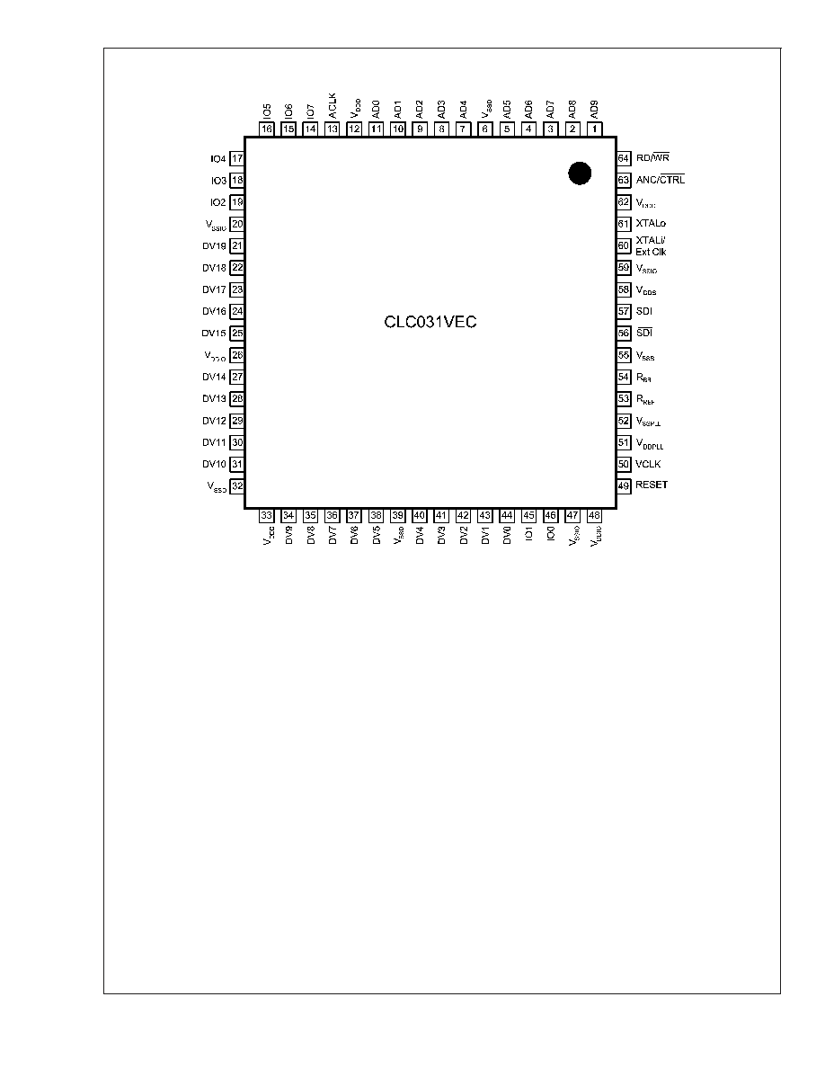
Ordering Information
Order Number
Package Type
NS Package Number
CLC031VEC
64-Pin TQFP
VEC-64A
PRELIMINARY
August 2003
CLC031
SMPTE
292M/259M
Digital
V
ideo
Deserializer
/
Descrambler
with
V
ideo
and
Ancilliary
Data
FIFOs
© 2003 National Semiconductor Corporation
DS200201
www.national.com
Absolute Maximum Ratings
(Note 1)
It is anticipated that this device will not be offered in
a military qualified version. If Military/Aerospace speci-
fied devices are required, please contact the National
Semiconductor Sales Office / Distributors for availability
and specifications.
CMOS I/O Supply Voltage
(V
DDIO
≠V
SSIO
):
4.0V
SDI Supply Voltage
(V
DDSI
≠V
SSSI
):
4.0V
Digital Logic Supply Voltage
(V
DDD
≠V
SSD
):
3.0V
PLL Supply Voltage
(V
DDPLL
≠V
SSPLL
):
3.0V
CMOS Input Voltage
(Vi):
V
SSIO
-0.15V to
V
DDIO
+0.15V
CMOS Output Voltage
(Vo):
V
SSIO
-0.15V to
V
DDIO
+0.15V
CMOS Input Current (single input):
Vi = V
SSIO
-0.15V:
-5 mA
Vi = V
DDIO
+0.15V:
+5 mA
CMOS Output Source/Sink Current:
±
6 mA
I
BB
Output Current:
+300 µA
I
REF
Output Current:
+300 µA
SDI Input Voltage
(Vi):
V
SSSI
-0.15V to
V
DDSI
+0.15V
Package Thermal Resistance
JA
@
0 LFM Airflow
40.1∞C/W
JA
@
500 LFM Airflow
24.5∞C/W
JC
5.23∞C/W
Storage Temp. Range:
-65∞C to +150∞C
Junction Temperature:
+150∞C
Lead Temperature (Soldering 4
Sec):
+260∞C
ESD Rating (HBM):
>
2.5 kV
ESD Rating (MM):
>
250 V
Recommended Operating Conditions
Symbol
Parameter
Conditions
Reference
Min
Typ
Max
Units
V
DDIO
CMOS I/O Supply Voltage
V
DDIO
-V
SSIO
3.150
3.300
3.450
V
V
DDSD
SDI Supply Voltage
V
DDSI
-V
SSSI
V
DDD
Digital Logic Supply
Voltage
V
DDD
≠V
SSD
2.375
2.500
2.625
V
V
DDPLL
PLL Supply Voltage
V
DDPLL
≠V
SSPLL
T
A
Operating Free Air
Temperature
0
+70
∞C
Required Input Conditions
(Note 9)
Symbol
Parameter
Conditions
Reference
Min
Typ
Max
Units
V
IN
Input Voltage Range
All LVCMOS
Inputs
V
SSIO
V
DDIO
V
t
r
, t
f
Rise Time, Fall Time
10%≠90%
1.0
1.5
3.0
ns
BR
SDI
Serial Input Data Rate
SMPTE 259M, Level C
SDI, SDI
270
M
BPS
SMPTE 259M, Level D
360
SMPTE 344M
540
SMPTE 292M
1,483
SMPTE 292M
1,485
V
CM(SDI)
Common Mode Voltage
V
IN
= 100 mV
SDI, SDI
V
SSSI
+0.05V
V
DDSI
-0.05V
V
V
IN(SDI)
SDI Serial Input Voltage
100
800
880
mV
t
r
, t
f
Rise Time, Fall Time
20%≠80%, SMPTE 259M
Data Rates
720
800
880
ps
20%≠80%, SMPTE 292M
Data Rates
270
CLC031
www.national.com
5