 | –≠–ª–µ–∫—Ç—Ä–æ–Ω–Ω—ã–π –∫–æ–º–ø–æ–Ω–µ–Ω—Ç: CLC414-8 | –°–∫–∞—á–∞—Ç—å:  PDF PDF  ZIP ZIP |
CLC414
Quad, Low Power Monolithic Op Amp
General Description
The CLC414 is a low power, quad, monolithic operational
amplifier designed for intermediate gain applications where
power and cost per channel are of primary concern. Benefit-
ing from National's current feedback architecture, the
CLC414 offers a gain range of
±
1 to
±
10 while providing
stable, oscillation free operation without external compensa-
tion, even at unity gain.
Operating from
±
5V supplies, the CLC414 consumes only
25mW of power per channel, yet maintains a 90MHz small
signal bandwidth and a 1000V/µs slew rate. The CLC414
also provides wide channel isolation with its 70dB crosstalk
(input referred at 5MHz). Applications requiring a high den-
sity solution to high speed amplification such as active filters
and instrumentation diff amps will benefit from the CLC414's
four integrated, wideband op amps in one 14-pin package.
Commercial remote sensing applications and battery pow-
ered radio transceivers requiring high performance, low
power will find the CLC414 to be an attractive, cost effective
solution. In composite video switching and distribution appli-
cations, the CLC414 offers differential gain and phase per-
formance of 0.1%, 0.12∞ at 3.58MHz.
The lower power CLC414 and the wideband CLC415 are
quad versions of the CLC406. Both of these quads afford the
designer lower power consumption and lower cost per chan-
nel with the additional benefit of requiring less board space
per amplifier.
Construction using an advanced, complementary bipolar
process and National's proven current feedback architec-
ture, the CLC414 is available in several versions to meet a
variety of requirements.
Enhanced Solutions (Military/Aerospace)
SMD Number: 5962-91693
Space level versions also available.
For more information, visit http://www.national.com/mil
Features
n
90MHz small signal bandwidth
n
2mA quiescent current per amplifier
n
70dB channel isolation
@
5MHz
n
0.1%/0.12∞ differential gain/phase
n
16ns settling to 0.1%
n
100V/µs slew rate
n
3.3ns rise and fall time (2V
PP
)
n
70mA output current
Applications
n
Composite video distribution amps
n
HDTV amplifiers
n
RGB video amplifiers
n
CCD signal processing
n
Active filters
n
Instrumentation diff. amps
n
General purpose high density requirements
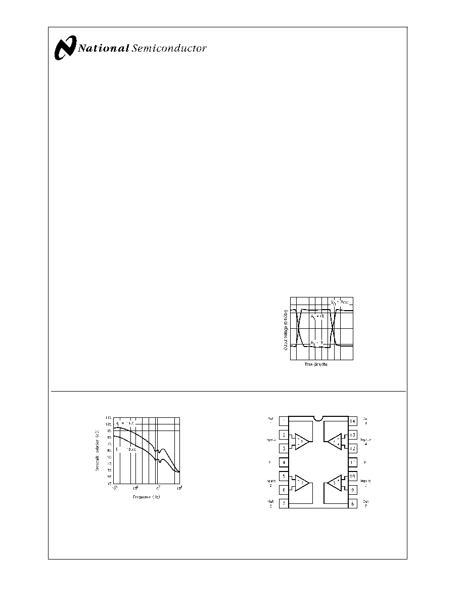
Small Signal Pulse Response
01275016
All-Hostile Crosstalk Isolation
01275007
Connection Diagram
01275015
Pinout
DIP & SOIC
December 2001
CLC414
Quad,
Low
Power
Monolithic
Op
Amp
© 2001 National Semiconductor Corporation
DS012750
www.national.com
Absolute Maximum Ratings
(Note 1)
If Military/Aerospace specified devices are required,
please contact the National Semiconductor Sales Office/
Distributors for availability and specifications.
Supply Voltage (V
CC
)
±
7V
I
OUT
Output is Short Circuit protected
to ground, but maximum reliability
will be maintained if I
OUT
does not
exceed...
70mA
Common Mode Input Voltage
±
V
CC
Differential Input Voltage
±
10V
Junction Temperature
+150∞C
Operating Temperature Range
-40∞C to +85∞C
Storage Temperature Range
-65∞C to +150∞C
Lead Temperature Range (Soldering
10 sec)
+300∞C
ESD Rating (Human Body Model)
<
1000V
Operating Ratings
Thermal Resistance
Package
(
JC
)
(
JA
)
MDIP
60∞C/W
110∞C/W
SOIC
45∞C/W
115∞C/W
Electrical Characteristics
(A
V
= +6, V
CC
=
±
5V, R
L
= 100
, R
f
= 500
; Unless Specified)
Symbol
Parameter
Conditions
Typ
Max/Min
(Note 2)
Units
Ambient Temperature
CLC414AJ
+25∞C
-40∞C
+25∞C
+85∞C
Frequency Domain Response
SSBW
-3dB Bandwidth
V
OUT
<
2V
PP
90
>
60
>
60
>
45
MHz
LSBW
V
OUT
<
5V
PP
55
>
35
>
40
>
35
MHz
Gain Flatness
V
OUT
<
2V
PP
GFPL
Peaking
DC to 15MHz
0
<
0.15
<
0.15
<
0.15
dB
GFPH
Peaking
>
15MHz
0
<
0.3
<
0.3
<
0.3
dB
GFR
Rolloff
DC to 30MHz
0.3
<
1.0
<
1.0
<
1.5
dB
LPD
Linear Phase Deviation
DC to 30MHz
0.8
<
1.2
<
1.2
<
1.5
deg
DG1
Differential Gain, A
V
= +2
R
L
= 150
, 3.58MHz
0.10
<
0.15
<
0.20
<
0.25
%
DG2
R
L
= 150
, 4.43MHz
0.12
<
0.20
<
0.25
<
0.30
%
DP1
Differential Phase, A
V
= +2
R
L
= 150
, 3.58MHz
0.12
<
0.15
<
0.20
<
0.50
deg
DP2
R
L
= 150
, 4.43MHz
0.15
<
0.20
<
0.25
<
0.60
deg
XT
Crosstalk Input Referred
5MHz (All Hostile)
60
<
58
<
58
<
56
dB
CXT
5MHz (Chan. to Chan.)
70
<
63
<
63
<
61
dB
Time Domain Response
TRS
Rise and Fall Time
2V Step
3.3
<
5.0
<
5.0
<
6.5
ns
TRL
5V Step
4.0
<
7.0
<
6.0
<
7.0
ns
TS1
Settling Time
to
±
0.1%
2V Step
16
<
24
<
24
<
30
ns
TS2
to 0.02%
2V Step
60
<
80
<
80
<
100
ns
OS
Overshoot
2V Step
5
<
10
<
10
<
10
%
SR
Slew Rate
1000
>
600
>
600
>
480
V/µs
Distortion And Noise Response
HD2
2nd Harmonic Distortion
2V
PP
, 5MHz
-47
<
-41
<
-41
<
-37
dBc
HD3
3rd Harmonic Distortion
2V
PP
, 5MHz
-55
<
-47
<
-47
<
-45
dBc
Equivalent Noise Input
VN
Non-Inverting Voltage
>
1MHz
4.2
<
5.0
<
5.0
<
5.5
nV/
ICN
Inverting Current
>
1MHz
9.8
<
11.8
<
11.8
<
13.0
pA/
NCN
Non-Inverting Current
>
1MHz
1.3
<
1.6
<
1.6
<
1.8
pA/
SNF
Total Noise Floor
>
1MHz
-154
<
-153
<
-153
<
-152
dBm
1Hz
INV
Total Integrated Noise
>
1MHz to 75MHz
37
<
44
<
44
<
48
µV
CLC414
www.national.com
2
Electrical Characteristics
(Continued)
(A
V
= +6, V
CC
=
±
5V, R
L
= 100
, R
f
= 500
; Unless Specified)
Symbol
Parameter
Conditions
Typ
Max/Min
(Note 2)
Units
Static, DC Performance
VIO
Input Offset Voltage (Note 3)
2
<
10.5
<
6
<
14
mV
DVIO
Average Temperature Coefficient
30
<
80
-
<
80
µV/C∞
IBN
Input Bias Current (Note 3)
Non-Inverting
1
<
10
<
5
<
5
µA
DIBN
Average Temperature Coefficient
20
<
75
≠
<
30
nA/∞C
IBI
Input Bias Current (Note 3)
Inverting
2
<
20
<
6
<
10
µA
DIBI
Average Temperature Coefficient
20
<
140
≠
<
75
nA/∞C
PSRR
Power Supply Rejection Ratio
50
>
46
>
46
>
44
dB
CMRR
Common Mode Rejection Ratio
50
>
45
>
45
>
43
dB
ICC
Supply Current (Note 3)
No Load
10
<
11.5
<
11.5
<
11.5
mA
Miscellaneous Performance
RIN
Non Inverting Input Resistance
2000
>
500
>
1000
>
1000
k
CIN
Non-Inverting Input Capacitance
1.0
<
2.0
<
2.0
<
2.0
pF
RO
Output Impedance
DC
0.2
<
0.6
<
0.3
<
0.2
VO
Output Voltage Range
R
L
= 100
±
2.8
±
2.5
±
2.6
±
2.7
V
CMIR
Common Mode Input Range
±
2.2
±
1.4
±
2.0
±
2.0
V
IO
Output Current
70
30
50
50
mA
Note 1: "Absolute Maximum Ratings" are those values beyond which the safety of the device cannot be guaranteed. They are not meant to imply that the devices
should be operated at these limits. The table of "Electrical Characteristics" specifies conditions of device operation.
Note 2: Max/min ratings are based on product characterization and simulation. Individual parameters are tested as noted. Outgoing quality levels are determined
from tested parameters.
Note 3: AJ-level: spec. is 100% tested at +25∞C.
Ordering Information
Package
Temperature Range
Industrial
Part Number
Package Marking
NSC Drawing
14-pin plastic DIP
-40∞C to +85∞C
CLC414AJP
CLC414AJP
N14A
14-pin plastic SOIC
-40∞C to +85∞C
CLC414AJE
CLC414AJE
M14A
CLC414
www.national.com
3
Typical Performance Characteristics
(T
A
= 25∞, A
V
= +6, V
CC
=
±
5V, R
L
= 100
, R
f
= 500
; Un-
less Specified).
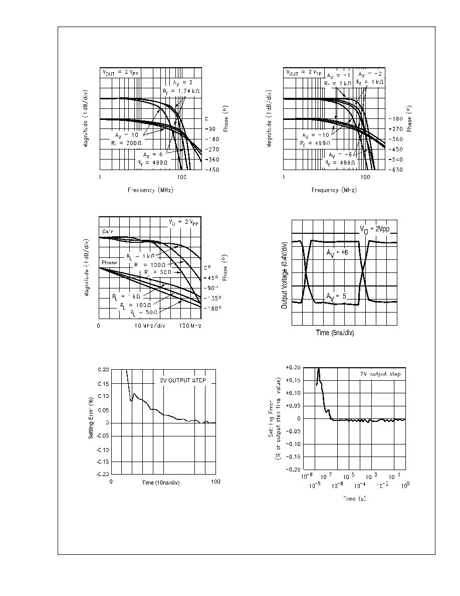
Non-Inverting Frequency Response
Inverting Frequency Response
01275001
01275002
Frequency Response for Various R
L
S
Small Signal Pulse Response
01275003
01275016
Short-Term Settling Time
Long-Term Settling Time
01275017
01275018
CLC414
www.national.com
4
Typical Performance Characteristics
(T
A
= 25∞, A
V
= +6, V
CC
=
±
5V, R
L
= 100
, R
f
= 500
;
Unless Specified). (Continued)
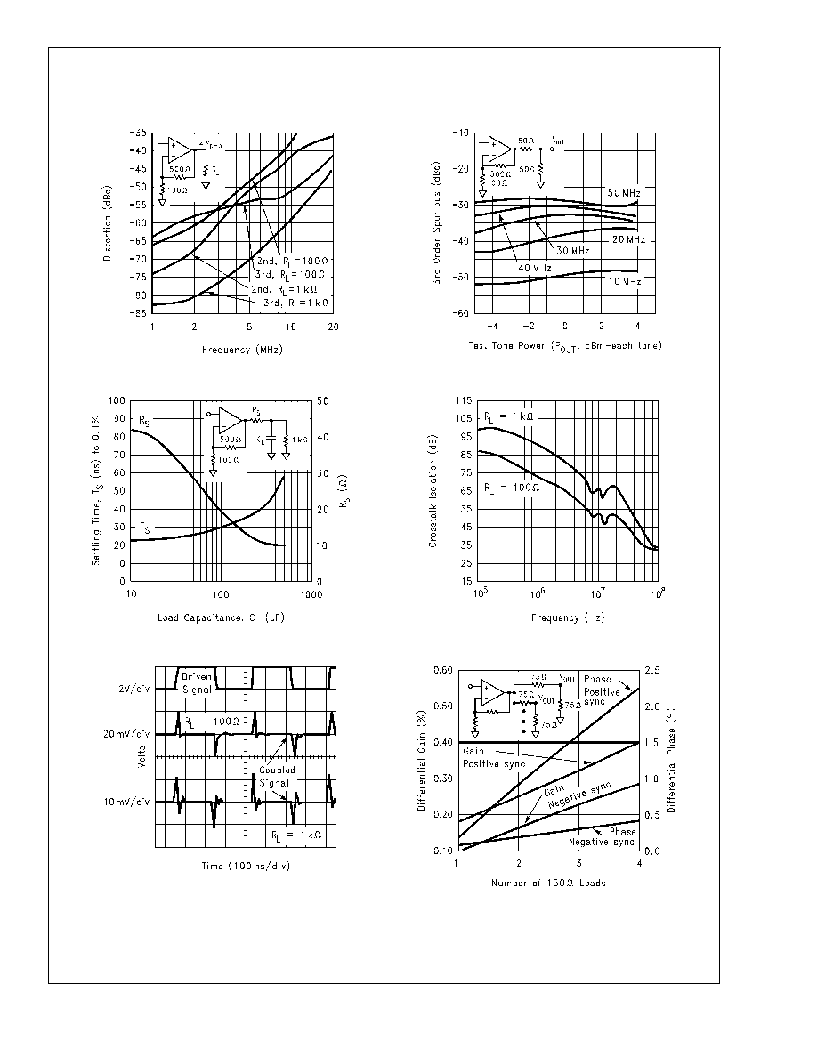
2nd and 3rd Harmonic Distortion
2-Tone, 3rd Order, Spurious Levels
01275004
01275005
Settling Time vs. Capacitive Load
All-Hostile Crosstalk Isolation
01275006
01275007
Most Susceptible Channel-Channel Pulse Coupling
Differential Gain and Phase (4.43 MHz, A
V
=+2)
01275008
01275009
CLC414
www.national.com
5