CLC425
Ultra Low Noise Wideband Op Amp
General Description
The CLC425 combines a wide bandwidth (1.9GBW) with a
very low input noise (1.05nV/
, 1.6pA/
) and low dc
errors (100µV V
OS
, 2µV/∞C drift) to provide a very precise,
wide dynamic range op amp offering closed-loop gains of
10.
Singularly suited for very wideband high gain operation, the
CLC425 employs a traditional voltage feedback topology
providing all the benefits of balanced inputs, such as low
offsets and drifts, as well as a 96dB open loop gain, a 100dB
CMRR and a 95dB PSRR.
The CLC425 also offers great flexibility with its externally
adjustable supply current, allowing designers to easily
choose the optimum set of power, bandwidth, noise and
distortion performance. Operating from
±
5V power supplies,
the CLC425 defaults to a 15mA quiescent current, or by
adding one external resistor, the supply current can be ad-
justed to less than 5mA.
The CLC425's combination of ultra low noise, wide gain
bandwidth, high slew rate and low dc errors will enable
applications in areas such as medical diagnostic ultrasound,
magnetic
tape
&
disk
storage,
communications
and
opto-electronics
to
achieve
maximum
high
frequency
signal-to-noise ratios.
Enhanced Solutions (Military/Aerospace)
SMD Number: 5962-93259
Space level versions also available.
For more information, visit http://www.national.com/mil
Features
n
1.9GHz gain-bandwidth product
n
1.05nV/
input voltage noise
n
0.8pA/
@
I
CC
5mA
n
100µV input offset voltage, 2µV/∞C drift
n
350V/µs slew rate
n
15mA to 5mA adjustable supply current
n
Gain range
±
10 to
±
1,000V/V
n
Evaluation boards & simulation macromodel
n
0.9dB NF
@
R
s
= 700
Applications
n
Instrumentation sense amplifiers
n
Ultrasound pre-amps
n
Magnetic tape & disk pre-amps
n
Photo diode transimpedance amplifiers
n
Wide band active filters
n
Low noise figure RF amplifiers
n
Professional audio systems
n
Low noise loop filters for PLLs
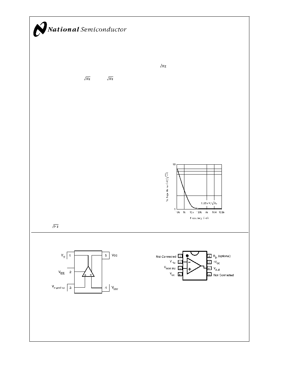
Equivalent Input Voltage Noise
01270853
Connection Diagrams
01270851
Pinout
SOT23-5
01270852
Pinout
DIP & SOIC
May 2001
CLC425
Ultra
Low
Noise
W
ideband
Op
Amp
© 2001 National Semiconductor Corporation
DS012708
www.national.com
Absolute Maximum Ratings
(Note 1)
If Military/Aerospace specified devices are required,
please contact the National Semiconductor Sales Office/
Distributors for availability and specifications.
Supply Voltage (V
CC
)
±
7V
I
OUT
Output is short circuit protected to
ground, but maximum reliability will
be maintained if I
OUT
does not
exceed...
125mA
Common Mode Input Voltage
±
V
CC
Maximum Junction Temperature
+150∞C
Operating Temperature Range
-40∞C to +85∞C
Storage Temperature Range
-65∞C to +150∞C
Lead Solder Duration (+300∞C)
10 sec
ESD rating (human body model)
1000V
Operation Ratings
Thermal Resistance
Package
(
JC
)
(
JA
)
MDIP
70∞C/W
125∞C/W
SOIC
65∞C/W
145∞C/W
SOT-23
115∞C/W
185∞C/W
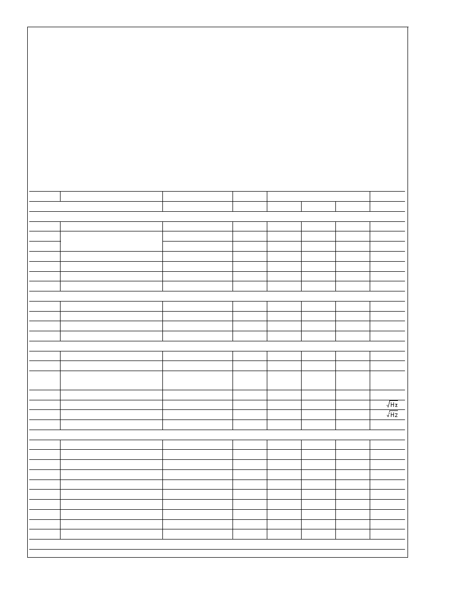
Electrical Characteristics
A
V
= +20, V
CC
=
±
5V, R
g
= 26.1
, R
L
= 100
, R
f
= 499
; unless specified
Symbol
Parameter
Conditions
Typ
Min/Max (Note 2)
Units
Ambient Temperature
CLC425AJ
+25∞C
-40∞C
+25∞C
+85∞
Frequency Domain Response
GBW
Gain Bandwidth Product
V
OUT
<
0.4V
PP
1.9
1.5
1.5
1.0
GHz
SSBW
-3dB Bandwidth
V
OUT
<
0.4V
PP
95
75
75
50
MHz
LSBW
V
OUT
<
5.0V
PP
40
30
30
20
MHz
Gain Flatness
V
OUT
<
0.4V
PP
GFP
Peaking
DC to 30MHz
0.3
0.7
0.5
0.7
dB
GFR
Rolloff
DC to 30MHz
0.1
0.7
0.5
0.7
dB
LPD
Linear Phase Deviation
DC to 30MHz
0.7
1.5
1.5
2.5
deg
Time Domain Response
TRS
Rise and Fall Time
0.4V Step
3.7
4.7
4.7
7.0
ns
TSS
Settling Time to 0.2%
2V Step
22
30
30
40
ns
OS
Overshoot
0.4V Step
5
12
10
12
%
SR
SlewRate
2V Step
350
250
250
200
V/µs
Distortion And Noise Response
HD2
2nd Harmonic Distortion
1V
PP
, 10MHz
-53
48
48
46
dBc
HD3
3rd Harmonic Distortion
1V
PP
, 10MHz
-75
65
65
60
dBc
IMD
3rd Order Intermodulation
Intercept
10MHz
35
dBm
Equivalent Input Noise
VN
Voltage
1MHz to 100MHz
1.05
1.25
1.25
1.8
nV/
ICN
Current
1MHz to 100MHz
1.6
4.0
2.5
2.5
pA/
NF
Noise Figure
R
s
= 700
0.9
dB
Static, DC Performance
AOL
Open Loop Gain
DC
96
77
86
86
dB
VIO
Input Offset Voltage (Note 3)
±
100
±
1000
±
800
±
1000
µV
DVIO
Average Drift
±
2
8
-
4
µV/∞C
IB
Input Bias Current (Note 3)
Non-Inverting
12
40
20
20
µA
DIB
Average Drift
-100
-250
-
-120
nA/∞C
IIO
Input Offset Current
±
0.2
3.4
2.0
2.0
µA
DIIO
Average Drift
±
3
±
50
-
±
25
nA/C∞
PSRR
Power Supply Rejection Ratio
DC
95
82
88
86
dB
CMRR
Common Mode Rejection Ratio
DC
100
88
92
90
dB
ICC
Supply Current (Note 3)
RL =
15
18
16
16
mA
Miscellaneous Performance
CLC425
www.national.com
3
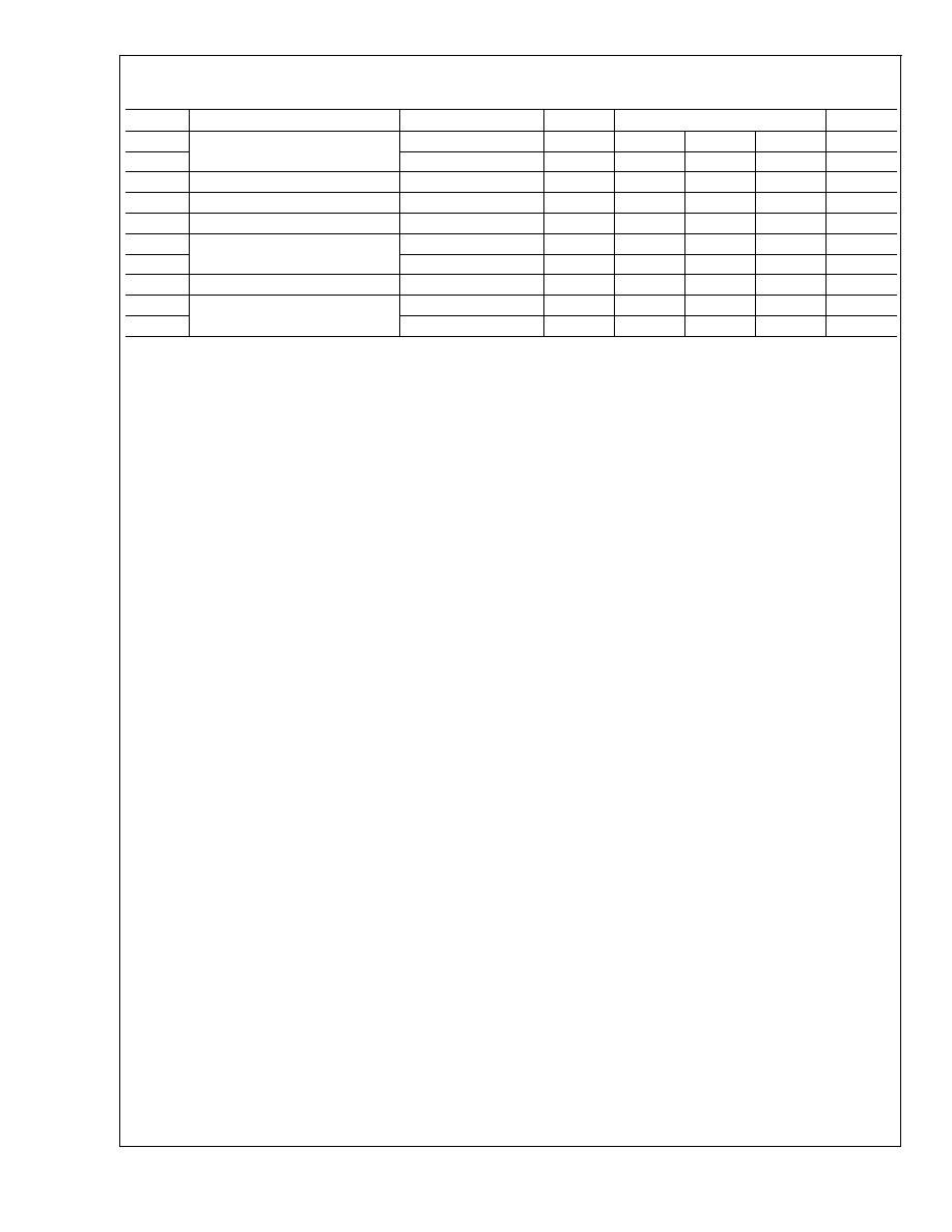
Electrical Characteristics
(Continued)
A
V
= +20, V
CC
=
±
5V, R
g
= 26.1
, R
L
= 100
, R
f
= 499
; unless specified
Symbol
Parameter
Conditions
Typ
Min/Max (Note 2)
Units
RINC
Input Resistance
Common-Mode
2
0.6
1.6
1.6
M
RIND
Differential-Mode
6
1
3
3
k
CINC
Input Capacitance
Common-Mode
1.5
2
2
2
pF
CIND
Differential-Mode
1.9
3
3
3
pF
ROUT
Output Resistance
Closed Loop
5
50
10
10
m
VO
Output Voltage Range
R
L
=
±
3.8
±
3.5
±
3.7
±
3.7
V
VOL
R
L
= 100
±
3.4
±
2.8
±
3.2
±
3.2
V
CMIR
Input Voltage Range
Common Mode
±
3.8
±
3.4
±
3.5
±
3.5
V
IOP
Output Current
Source
80
70
70
70
mA
ION
Sink
90
45
55
55
mA
Note 1: "Absolute Maximum Ratings" are those values beyond which the safety of the device cannot be guaranteed. They are not meant to imply that the devices
should be operated at these limits. The table of "Electrical Characteristics" specifies conditions of device operation.
Note 2: Max/min ratings are based on product characterization and simulation. Individual parameters are tested as noted. Outgoing quality levels are determined
from tested parameters.
Note 3: AJ-level: spec. is 100% tested at +25∞C, sample at 85∞C.
CLC425
www.national.com
4
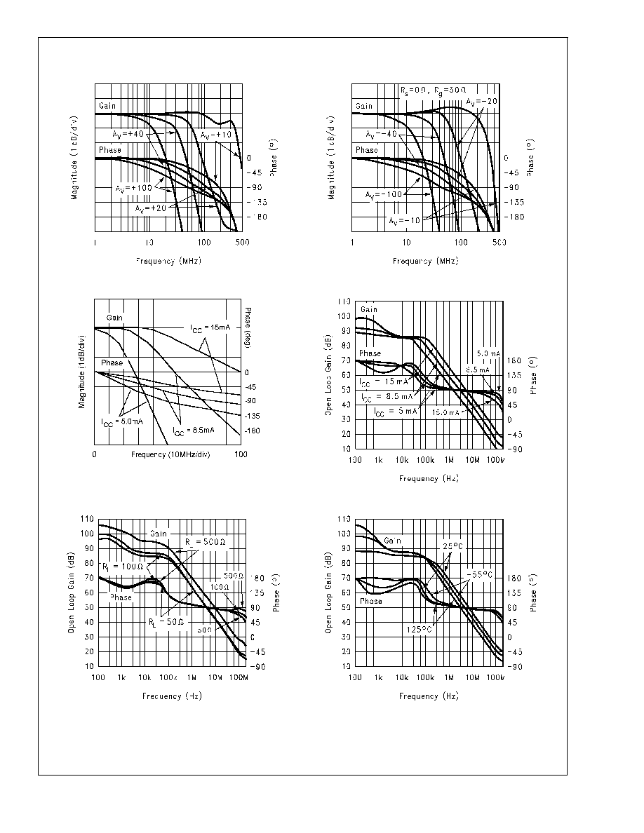
Typical Performance Characteristics
Non-Inverting Frequency Response
Inverting Frequency Response
01270801
01270802
Frequency Response vs. I
CC
(A
V
= +20)
Open Loop Gain and Phase vs. I
CC
01270803
01270804
Open Loop Gain and Phase vs. R
L
Open Loop Gain and Phase vs. Temp
01270805
01270806
CLC425
www.national.com
5