CLC426
Wideband, Low Noise, Voltage Feedback Op Amp
General Description
The National CLC426 combines an enhanced voltage feed-
back architecture with an advanced complimentary bipolar
process to provide a high speed op amp with very low noise
(1.6nV/
& 2.0pA/
) and distortion (-62dBc/-68dBc
2nd/3rd harmonics at 1V
PP
and 10MHz).
Providing a wide 230MHz gain bandwidth product, a fast
400V/µs slew rate and very quick 16ns settling time to
0.05%, the CLC426 is the ideal choice for high speed appli-
cations requiring a very wide dynamic range such as an
input buffer for high resolution analog-to-digital converters.
The CLC426 is internally compensated for gains
2V/V and
can easily be externally compensated for unity gain stability
in applications such as wideband low noise integrators. The
CLC426 is also equipped with external supply current adjust-
ment which allows the user to optimize power, bandwidth,
noise and distortion performance for each application.
The CLC426's combination of speed, low noise and distor-
tion and low dc errors will allow high speed signal condition-
ing applications to achieve the highest signal-to-noise per-
formance. To reduce design times and assist board layout,
the CLC426 is supported by an evaluation board and SPICE
simulation model available from National.
For even higher gain-bandwidth voltage-feedback op amps
see the 1.9GHz CLC425 (A
V
10V/V) or the 5.0GHz
CLC422 (A
V
30V/V).
Enhanced Solutions (Military/Aerospace
SMD Number: 5962-94597
*
Space level versions also available.
*
For more information, visit http://www.national.com/mil
Features
n
Wide gain-bandwidth product: 230MHz
n
Ultra low input voltage noise: 1.6nV/
n
Very low harmonic distortion: -62/-68dBc
n
Fast slew rate: 400V/µs
n
Adjustable supply current
n
Dual
±
2.5 to
±
5V or single 5 to 12V supplies
n
Externally compensatable
Applications
n
Active filters & integrators
n
Ultrasound
n
Low power portable video
n
ADC/DAC buffer
n
Wide dynamic range amp
n
Differential amps
n
Pulse/RF amp
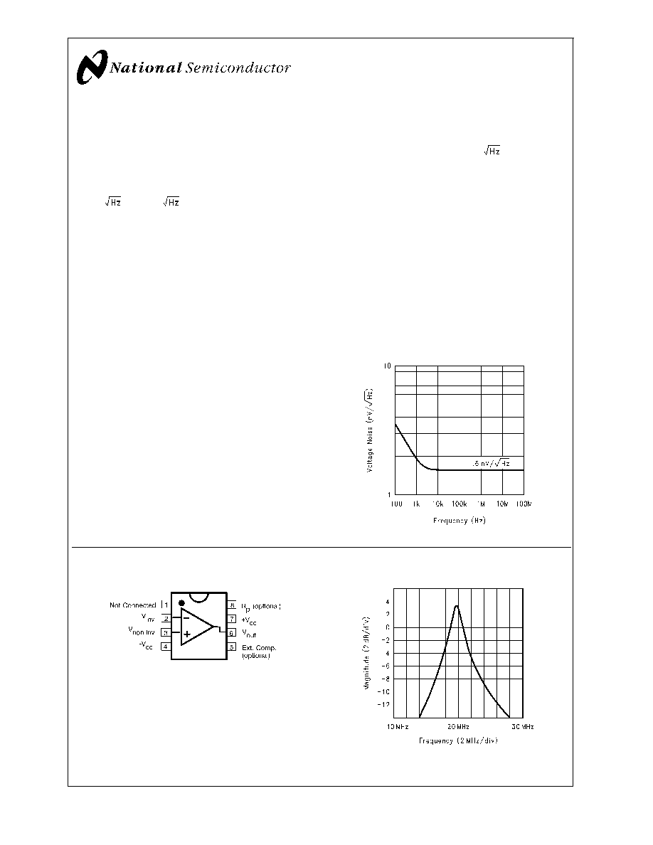
Connection Diagram
Input Voltage Noise Density
DS012709-1
DS012709-4
Pinout
DIP & SOIC
Frequency Response
DS012709-3
July 2001
CLC426
W
ideband,
Low
Noise,
V
oltage
Feedback
Op
Amp
© 2001 National Semiconductor Corporation
DS012709
www.national.com
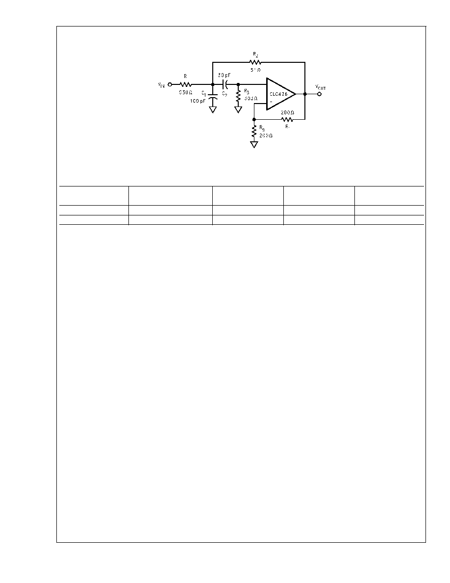
Typical application
Ordering Information
Package
Temperature Range
Industrial
Part Number
Package Marking
NSC Drawing
8-Pin Plastic DIP
-40∞C to +85∞C
CLC426AJP
CLC426AJP
N08E
8-Pin Plastic SOIC
-40∞C to +85∞C
CLC426AJE
CLC426AJE
M08A
DS012709-2
Wide Dynamic Range Sallen-Key Band Pass Filter 2nd-Order (20MHz, Q = 10, G = 2)
CLC426
www.national.com
2
Absolute Maximum Ratings
(Note 1)
If Military/Aerospace specified devices are required,
please contact the National Semiconductor Sales Office/
Distributors for availability and specifications.
Supply Voltage
±
7V
Short Circuit Current
(Note 6)
Common-Mode Input Voltage
±
V
cc
Differential Input Voltage
±
10V
Maximum Junction Temperature
+150∞C
Storage Temperature
-65∞C to +150∞C
Lead Temperature (Soldering 10 sec)
+300∞C
ESD
2000V
Electrical Characteristics
(V
CC
=
±
5; A
V
= +2V/V; R
f
= 100
; R
L
= 100
; unless noted)
Notes
Parameters
Conditions
Typ
Max/Min Ratings (Note 2)
Units
Ambient Temperature
CLC426
+25∞C
+25∞C
0
to+70∞C
-40
to+85∞C
Frequency Domain Response
Gain Bandwidth Product
V
OUT
<
0.5V
PP
230
170
120
100
MHz
(Note 4),
(Note 5),
(Note 8)
-3dB Bandwidth, A
V
= +2
V
OUT
<
0.5V
PP
130
90
70
55
MHz
V
OUT
<
5.0V
PP
50
25
22
20
MHz
Gain Flatness
V
OUT
<
0.5V
PP
(Note 4),
(Note 8)
Peaking
DC to 200MHz
0.6
1.5
2.2
2.5
dB
(Note 4),
(Note 8)
Rolloff
DC to 30MHz
0.0
0.6
1.0
1.0
dB
Linear Phase Deviation
DC to 30MHz
0.2
1.0
1.5
1.5
deg
Time Domain Response
Rise and Fall Time
1V Step
2.3
3.5
5.0
6.5
ns
Settling Time
2V Step to 0.05%
16
20
24
24
ns
Overshoot
1V Step
5
15
15
18
%
Slew Rate
5V Step
400
300
275
250
V/µs
Distortion And Noise Response
(Note 3)
2nd Harmonic Distortion
1V
PP
,10MHz
-62
-52
-47
-45
dBc
(Note 3)
3rd Harmonic Distortion
1V
PP
,10MHz
-68
-58
-54
-54
dBc
Equivalent Input Noise
Op Amp Only
Voltage
1MHz to 100MHz
1.6
2.0
2.3
2.6
nV/
Current
1MHz to 100MHz
2.0
3.0
3.6
4.6
pA/
Static DC Performance
Open-Loop Gain
DC
64
60
54
54
dB
(Note 3)
Input Offset Voltage
1.0
2.0
2.8
2.8
mV
Average Drift
3
≠
10
10
µV/∞C
(Note 3)
Input Bias Current
5
25
40
65
µA
Average Drift
90
≠
600
700
nA/∞C
(Note 3)
Input Offset Current
0.3
3
5
5
µA
Average Drift
5
≠
25
50
nA/∞C
(Note 4)
Power-Supply Rejection Ratio
DC
73
65
60
60
dB
Common-Mode Rejection Ratio
DC
70
62
57
57
dB
(Note 3)
Supply Current
Pin #8 Open,
R
L
=
11
12
13
15
mA
Miscellaneous Performance
Input Resistance
Common-Mode
500
250
125
125
k
Differential-Mode
750
200
50
25
k
Input Capacitance
Common-Mode
2.0
3.0
3.0
3.0
pF
Differential-Mode
2.0
3.0
3.0
3.0
pF
CLC426
www.national.com
3

Electrical Characteristics
(Continued)
(V
CC
=
±
5; A
V
= +2V/V; R
f
= 100
; R
L
= 100
; unless noted)
Notes
Parameters
Conditions
Typ
Max/Min Ratings (Note 2)
Units
Miscellaneous Performance
Output Resistance
Closed Loop
0.07
0.1
0.2
0.2
Output Voltage Range
R
L
=
±
3.8
±
3.5
±
3.3
±
3.3
V
R
L
= 100
±
3.5
±
3.2
±
2.6
±
1.3
V
Input Voltage Range
Common Mode
±
3.7
±
3.5
±
3.3
±
3.3
V
Output Current
±
70
±
50
±
40
+35,
-20
mA
Note 1: "Absolute Maximum Ratings" are those values beyond which the safety of the device cannot be guaranteed. They are not meant to imply that the devices
should be operated at these limits. The table of "Electrical Characteristics" specifies conditions of device operation.
Note 2: Min/max ratings are based on product characterization and simulation. Individual parameters are tested as noted. Outgoing quality levels are determined
from tested parameters.
Note 3: J-level: spec. is 100% tested at +25∞C, sample at 85∞C. L-level: spec. is 100% wafer probed at 25∞C.
Note 4: J-level: spec is sample tested at 25∞C
Note 5: Minimum table stable gain with out external compensation is +2 or -1V/V, the CLC426 unity-gain stable with external compensation.
Note 6: Output is short circuit protected to ground, however maximum reliability is obtained if output current does not exceed 160mA
Note 7: See test for compensation techniques.
Note 8: Spec is guaranteed to 0.5V
PP
but tested with 0.1V
PP
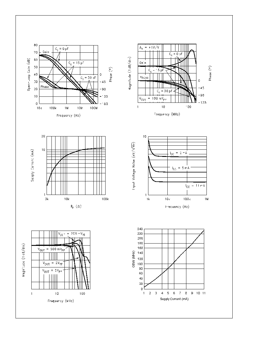
Typical Performance Characteristics
(T
A
= 25∞C,
±
V
CC
=
±
5V, A
V
= +2, R
f
= 100
, R
L
= 100
,
unless noted)
Non-Inverting Frequency Response
DS012709-5
Inverting Frequency Response
DS012709-6
Frequency Response vs. Load Resistance
DS012709-7
Open-Loop Gain vs. Supply Current
DS012709-8
CLC426
www.national.com
4
Typical Performance Characteristics
(T
A
= 25∞C,
±
V
CC
=
±
5V, A
V
= +2, R
f
= 100
, R
L
= 100
,
unless noted) (Continued)
Open-Loop Gain vs. Compensation Cap.
DS012709-9
Frequency Response vs. Compensation Cap.
DS012709-10
Supply Current vs. Rp
DS012709-11
Voltage Noise vs. Supply Current
DS012709-12
Frequency Response vs. Output
Amplitude
DS012709-13
Gain-Bandwidth Product vs Supply Current
DS012709-14
CLC426
www.national.com
5