 | –≠–ª–µ–∫—Ç—Ä–æ–Ω–Ω—ã–π –∫–æ–º–ø–æ–Ω–µ–Ω—Ç: CLC522AMC | –°–∫–∞—á–∞—Ç—å:  PDF PDF  ZIP ZIP |
N
CLC522
Wideband Variable-Gain Amplifier
General Description
The CLC522 variable gain amplifier (VGA) is a dc-coupled, two-
quadrant multiplier with differential voltage inputs and a single-ended
voltage output. Two input buffers and an output operational amplifer
are integrated with the multiplier core to make the CLC522 a complete
VGA system that does not require external buffering.
The CLC522 provides the flexibility of externally setting the maximum
gain with only two external resistors. Greater than 40dB gain control
is easily achieved through a single high impedance voltage input. The
CLC522 provides a linear (in Volts per Volt) relationship between the
amplifier's gain and the gain-control input voltage.
The CLC522's maximum gain may be set anywhere over a nominal
range of 2V/V to 100V/V. The gain control input then provides
attenuation from the maximum setting. For example, set for a
maximum gain of 100V/V, the CLC522 will provide a 100V/V to 1V/V
gain control range by sweeping the gain control input voltage from +1
to -0.98V.
Set at a maximum gain of 10V/V, the CLC522 provides a 165MHz
signal channel bandwidth and a 165MHz gain control bandwidth. Gain
nonlinearity over a 40dB gain range is 0.5% and gain accuracy at
A
V
max
= 10V/V is typically ±0.3%.
June 1999
CLC522
Wideband V
a
riab
le-Gain
Amplifier
Features
s
330MHz signal bandwidth: A
vmax
= 2
s
165MHz gain-control bandwidth
s
0.3∞ to 60MHz linear phase deviation
s
0.04% (-68dB) signal-channel non-linearity
s
>40dB gain-adjustment range
s
Differential or single-end voltage inputs
s
Single-ended voltage output
Applications
s
Variable attenuators
s
Pulse amplitude equalizers
s
HF modulators
s
Automatic gain control & leveling loops
s
Video production switching
s
Differential line receivers
s
Voltage controlled filters
©
1999 National Semiconductor
Corporation
http://www.national.com
Printed in the U.S.A.
Gain
(V/V)
Gain vs. Gain Control Voltage (V
g
)
-1.1
Gain Control Voltage, V
g
(Volts)
1.1
10
0
V
V
n
s
CR
s
s
CR
k
C R
k
R
R
Q
k R
R
k
CR
o
in
b
b
y
f
g
b
y
o
y
= -
+
+
=
=
=
1
1
1
185
2
2
2
.
,
,
T
T
T
T
Typical Application
ypical Application
ypical Application
ypical Application
ypical Application
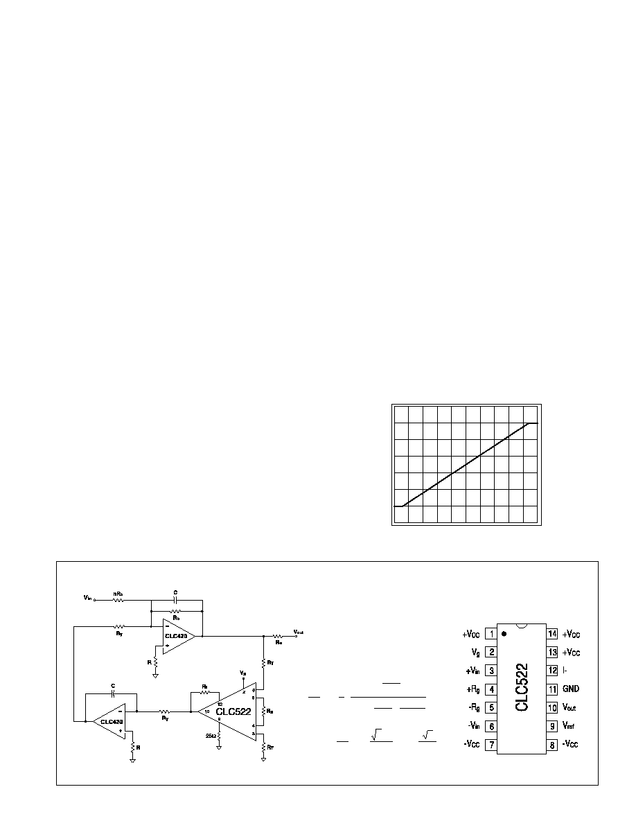
2nd Order Tuneable Bandpass Filter
Pinout
DIP & SOIC
CLC522 Electrical Characteristics
(V
CC
= ±5V; A
Vmax
= +10; R
f
=1k
; R
g
=182W; R
L
= 100
; V
g
=+1.1V)
Ordering Information
supply voltage
±7V
short circuit current
80mA
common-mode input voltage
±V
cc
maximum junction temperature
+150
∞
C
storage temperature
-65∞C to+150∞C
lead temperature (soldering 10 sec)
+300∞C
transistor count
74
Absolute Maximum Ratings
Notes
1) AJE (SOIC) is tested/guaranteed with R
f
=866
and R
g
= 165
.
2) J-level, spec is 100% tested at +25∞C.
3) Specified with V
in
= 0.2V and V
g
< 0.5V
pp
.
4) Feedtrough is specified at max. attenuation (i.e V
g
=-1.1V)
http://www.national.com
2
Model
Temperature Range
Description
CLC522AJP
-40∞C to +85∞C
14-pin PDIP
CLC522AJE
-40∞C to +85∞C
14-pin SOIC
CLC522ALC
-40∞C to +85∞C
dice
CLC522AMC
-55∞C to +125∞C
dice, MIL-STD-883
PARAMETERS
CONDITIONS
TYP
MIN/MAX RATINGS
UNITS
NOTES
Ambient Temperature
AJ
+25
+25
0 to +70
-40 to +85
∞C
1
FREQUENCY DOMAIN RESPONSE
-3dB bandwidth
V
out
< 0.5V
pp
165
120
115
110
MHz
V
out
< 5.0V
pp
150
100
95
90
MHz
gain control bandwidth
V
out
< 0.5V
pp
165
120
115
110
MHz
3
gain flatness
V
out
< 0.5V
pp
peaking
DC to 30MHz
0
0.1
0.1
0.1
dB
rolloff
DC to 30MHz
0.05
0.25
0.25
0.4
dB
linear phase deviation
DC to 60MHz
0.3
1.0
1.1
1.2
∞
feedthrough
30MHz
- 62
- 57
- 57
-57
dB
4
TIME DOMAIN RESPONSE
rise and fall time
0.5V step
2.2
2.9
3.0
3.2
ns
5.0V step
3.0
5.0
5.0
5.0
ns
settling time
2.0V step to 0.1%
12
18
18
18
ns
overshoot
0.5V step
2
15
15
15
%
slew rate
4.0V step
2000
1400
1400
1400
V/
µ
s
DISTORTION AND NOISE RESPONSE
2
nd
harmonic distortion
2V
pp
, 20MHz
- 50
- 44
- 44
-44
dBc
3
rd
harmonic distortion
2V
pp
, 20MHz
- 65
- 58
- 56
-54
dBc
equivalent input noise
1 to 200MHz
5.8
6.2
6.5
6.8
nV/
Hz
noise floor
1 to 200MHz
- 152
- 150
- 149
- 149
dBm
1Hz
GAIN ACCURACY
signal channel nonlinearity (
SGNL
) V
out
= ±2V
pp
0.04
0.1
0.1
0.1
%
2
gain control nonlinearity (
GCNL
)
full range
0.5
2.0
2.2
3.0
%
2
gain error (
GACCU
)
A
V
max
=+10
± 0.0
± 0.5
± 0.5
± 1.0
dB
2
V
g
high
+ 990
+ 990±60
+ 990±60
+ 990±60
mV
low
- 975
- 975±80
- 975±80
- 975±80
mV
STATIC DC PERFORMANCE
V
in
voltage range
common mode
± 2.2
± 1.2
± 1.2
± 1.4
V
bias current
9
21
26
45
µ
A
2
average drift
65
---
175
275
nA/∞C
offset current
0.2
2.0
3.0
4.0
µ
A
average drift
5
---
30
40
nA/∞C
resistance
1500
650
450
175
k
capacitance
1.0
2.0
2.0
2.0
pF
V
g
bias current
15
38
47
82
µ
A
average drift
125
---
300
600
nA/∞C
resistance
100
38
30
15
k
capacitance
1.0
2.0
2.0
2.0
pF
output voltage range
R
L
=
± 4.0
± 3.7
± 3.6
± 3.5
V
current
± 70
± 47
± 40
± 25
mA
offset voltage
A
V
max
=+10
25
85
95
120
mV
2
average drift
100
---
350
400
µ
V/∞C
resistance
0.1
0.2
0.3
0.6
I
Rgmax
1.8
1.37
1.26
1.15
mA
power supply sensitivity
output referred
10
40
40
40
mV/V
common-mode rejection ratio
input referred
70
59
59
59
dB
supply current
R
L
=
46
61
62
63
mA
2
Min/max ratings are based on product characterization and simulation. Individual parameters are tested as noted. Outgoing quality levels are
determined from tested parameters.
Package Thermal Resistance
Package
JC
JA
Plastic (AJP)
55∞C/W
100∞C/W
Surface Mount (AJE)
35∞C/W
105∞C/W
CerDIP
40∞C/W
95∞C/W
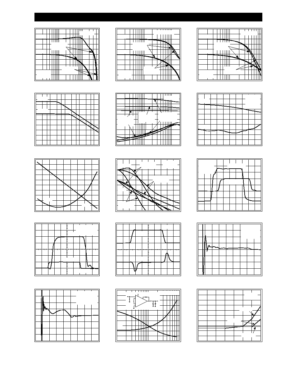
CLC522 Typical Performance
(T
A
=+25
∞
C, V
cc
=
±
5V, A
v
=+10, V
g
=1.1V, R
L
=100
; unless noted)
0
-45
-90
-135
-180
-270
V
out
= 500m V
pp
R
g
=182
R
f
= 1k
A
V
=A
Vmax
(V
g
=1.0V)
A
V
=1
(V
g
=-0.8V)
Gain
Phase
1
Frequency (MHz)
200
Nor
m
al
i
z
ed
M
a
gni
t
ude
(1dB/di
v
)
P
h
a
s
e (
4
5
∞
/div)
Frequency Response (A
Vmax
=10)
V
in
= 25mV
pp
R
g
=10.2
R
f
= 715
A
V
=A
Vmax
(V
g
=1.0V)
Gain
Phase
1
Frequency (MHz)
100
N
o
rma
lize
d
Ma
g
n
itu
d
e
(1
d
B
/d
iv)
P
h
a
s
e (
4
5
∞
/div)
Frequency Response (A
Vmax
=100)
0
-45
-90
-135
-180
-270
A
V
=1
(V
g
=-0.98V)
V
out
= 2V
pp
R
g
=2k
R
f
= 2.2k
A
V
=A
Vmax
(V
g
=1.0V)
Gain
Phase
1
Frequency (MHz)
500
Nor
m
al
i
z
ed
M
a
gni
tude
(1dB/di
v
)
P
h
a
s
e (
4
5
∞
/div)
Frequency Response (A
Vmax
=2)
0
-45
-90
-135
-180
-270
A
V
=1
(V
g
=0V)
100
90
80
70
60
50
40
30
20
10
0
Frequency (Hz)
PSRR/CM
RR
(dB)
PSRR and CMRR (Input Referred)
CMRR
PSRR
10
4
10
5
10
6
10
7
10
8
P h a s e
G a i n
A
vmax
+ 10
V
o
= 2V
pp
R
f
= 1k
V
g
= 1.1V
M
a
gni
tude
(0.1dB/di
v
)
Devi
ati
o
n
fr
om
L
i
near
P
h
ase(
0.1
∞
/div)
Gain Flatness & Linear Phase Deviation
0
Frequency (3MHz/div)
30MHz
V
g
(Volts)
0.20
0.18
0.16
0.14
0.12
0.10
0.08
0.06
0.04
0.02
0.00
10
0
F
u
l
l
Scal
e
N
on-
l
i
near
i
t
y
(
%
)
Gain
(V/V)
SGNL vs. V
g
, Gain
0.9
0.7
0.5
0.3
0.1 -0.1 -0.3 -0.5 -0.7 -0.9
Frequency (25MHz/div)
0
-45
-90
-135
-180
-225
M
agni
tude
(1dB/di
v
)
Large Signal Frequency Response
Magnitude
Phase
Gain
SGNL
V
o
= 5V
pp
V
g
= 1.1V
A
vmax
= +100
R
f
= 806
A
vmax
= +2
R
f
= 2k
A
vmax
= +10
R
f
= 1k
0
250
Phase
(deg)
R
f
= 1k
V
out
= 0.5V
pp
V
o u t
= 5V
p p
A
vmax
= +10
V
g
=1.0V
Lar
ge
si
gnal
(
V
ol
ts)
Sm
al
l
Si
gnal
(
V
ol
ts)
Large & Small Signal Pulse Response
T i m e
( 5 n s / d i v )
3
2
1
0
-1
-2
-3
+.75
+.50
+.25
0
-.25
-.50
-.75
V
o u t
V
g
V
g
= 1.0V
V
g
= -1.0V
A
vmax
= + 10
V
in
= 0.25V DC
2.5
Vo
u
t
(
0
.
5
V
/
d
i
v.
)
Gain Control Settling Time & Delay
Time
(5ns/div)
0
100m
V/di
v
Gain Control Channel Feedthrough
Time
(5ns/div)
+1V
0
-1V
V
g
Input
Output
V
in
= 0
A
Vmax
= + 10
2V output step
V
g
= 1.0V
.2
.15
0.1
.05
0
-.05
-.1
-.15
-.2
S
e
t
t
l
i
n
g E
r
r
o
r (
%
)
Short Term Settling Time
0
100
Time (10ns/div)
A
Vmax
= + 10
2V output step
V
g
= 1.0V
.20
.15
.10
.05
0
-.05
-.10
-.15
-.20
S
e
t
t
l
i
n
g E
r
r
o
r (
%
)
Long Term Settling Time
1 0
- 9
1 0
- 8
1 0
- 7
1 0
- 6
1 0
- 5
1 0
- 4
1 0
- 3
1 0
- 2
1 0
- 1
1 0
0
Time (sec)
Rs
Ts
A
vmax
= +10
Load Capacitance, C
L
(pF)
S
e
t
t
l
i
n
g T
i
m
e
, T
S
, (
n
s
)
, t
o
0
.
1
%
Rs
(
ohm
s)
Settling Time vs. Capacitive Load
10
100
1000
50
40
30
20
10
0
100
90
80
70
60
50
40
30
20
10
0
R
s
C
L
Vg=1.0Volt
50
182
1k
1k
CLC522
Frequency (MHz)
V
g
=+1
.
1
V
V
g
=
-
1.1V
55
40
25
10
-5
-20
-35
-50
-65
-80
-95
Gain
(dB)
F e e d - t h r o u g h I s o l a t i o n
1 10 10 0
A
V m a x
= + 2
R
f
= 2 k
A
V m a x
= + 1 0
R
f
= 1 k
A
V m a x
= + 1 0 0
R
f
= 7 5 0
V
o
= 2 . 5 V
p p
50
45
40
35
30
25
20
15
10
5
0
0
2
4
6
8
10
12
14
S
e
t
t
l
i
n
g T
i
m
e
t
o
0
.
1
%
(
n
s
)
Settling Time vs. Gain
Attenuation From Maximum Gain (dB)
R
f
= 2k
V
o
= 1V
pp
A
vmax
= 5
A
vmax
= 10
A
vmax
= 20
3
http://www.national.com
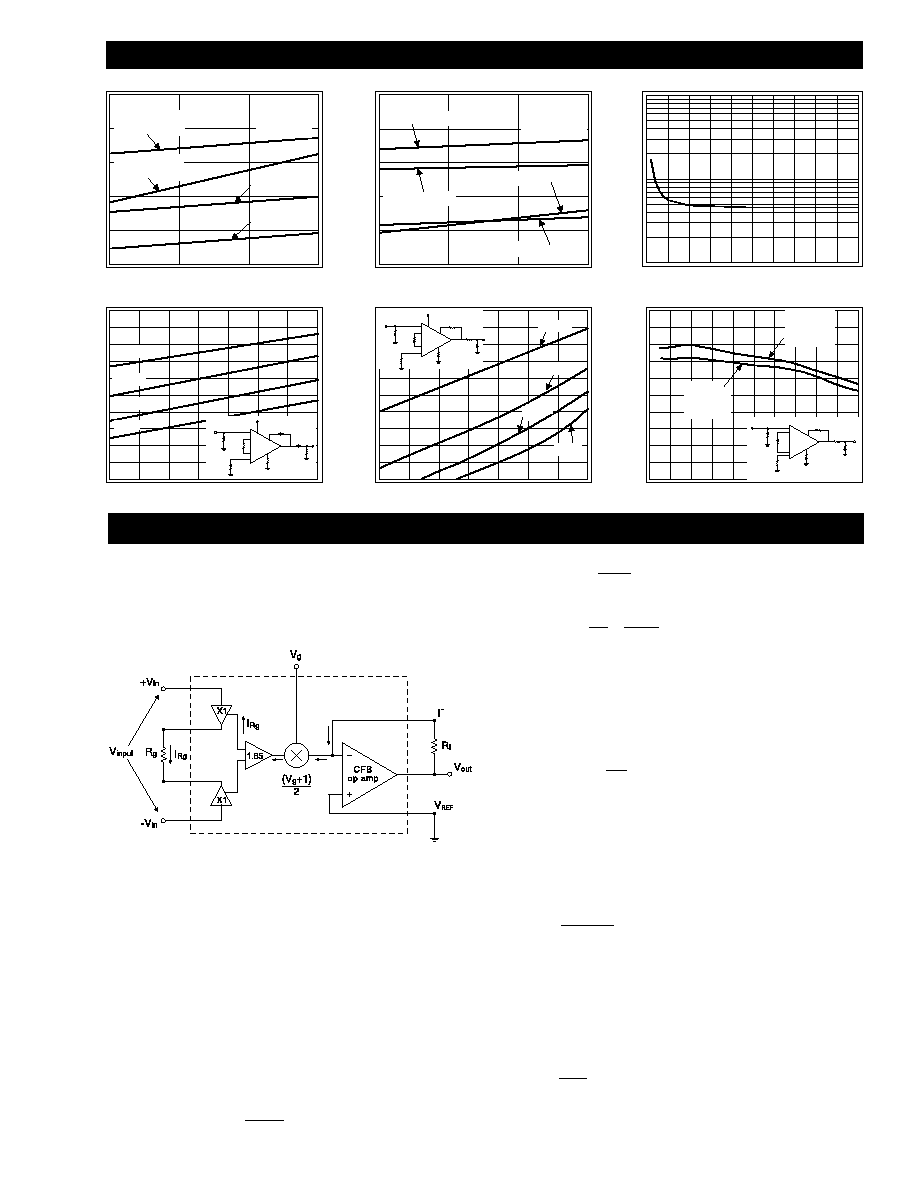
Theory of Operation
The CLC522 is a linear wideband variable-gain amplifier
as illustrated in Fig 1. A voltage input signal may be
applied differentially between the two inputs (+V
in
, -V
in
),
or single-endedly by grounding one of the unused inputs.
The CLC522 input buffers convert the input voltage to a
current (I
Rg
) that is a function of the differential input
voltage (V
input
=+V
in
- -V
in
) and the value of the gain-
setting resistor (R
g
). This current (I
Rg
) is then mirrored to
a gain stage with a current gain of 1.85. The voltage-
controlled two-quadrant multiplier attenuates this current
which is then converted to a voltage via the output
amplifier. This output amplifier is a current-feedback op
amp configured as a transimpedance amplifier. It's tran-
simpedance gain is the feedback resistor (R
f
). The input
signal, output, and gain control are all voltages. The
output voltage can easily be calculated as seen in Eq. 1.
Eq. 1
Fig. 1
Phase
Negative Sync
Phase
Positive Sync
Gain
Positive Sync
Gain
Negative Sync
4.43 MHz
A
vmax
= +10
V
g
= 1.0V
N u m b e r o f 1 5 0
L o a d s
Di
f
f
er
enti
al
G
a
i
n
(%
)
Di
f
f
er
enti
al
Phase
(degr
e
es)
Differential Gain and Phase
1
2
3
4
.25
.20
.15
.10
.05
0
.25
.20
.15
.10
.05
0
50MHz
20MHz
10MHz
5MHz
-4
-2
0
2
4
6
8
10
Output Power (Pout, dBm)
-35
-40
-45
-50
-55
-60
-65
-70
-75
-80
-85
D
i
stortion
L
e
vel
(
d
Bc)
2nd Harmonic Distortion vs. P
out
1.1V
50
P
o
1k
50
50
50
20
182
R
f
V
g
522
50MHz
20MHz
10MHz
5MHz
-4
-2
0 2
4
6
8
10
Output Power (Pout, dBm)
-35
-40
-45
-50
-55
-60
-65
-70
-75
-80
-85
D
i
stortion
L
e
vel
(
d
Bc)
3rd Harmonic Distortion vs. P
out
1.1V
50
50
1k
50
50
20
182
R
f
V
g
522
P
o
Input
Limited
R
f
= 900
Output
Limited
R
f
= 1.4k
0
100
Frequency (MHz)
20
19
18
17
16
15
14
13
12
11
10
-1
d
B
C
o
mp
re
ssio
n
(d
B
m
)
-1dB Compression at Maximum Gain
P
o
P
i
R
g
R
f
50
50
50
20
50
522
CLC522 Typical Performance
(T
A
=+25
∞
C, V
cc
=
±
5V, A
v
=+10, V
g
=1.1V, R
L
=100
; unless noted)
Phase, V
g
= 0.0V
Phase, V
g
= 1.0V
Gain, V
g
= 0.0V
Gain, V
g
= 1.0V
4.43 MHz
Positive Sync
A
vmax
= +2
Number of 150
Loads
Di
f
f
er
enti
al
G
a
i
n
(%
)
Dif
f
erent
ialP
hase
(degrees)
Differential Gain and Phase
1
2
3
4
.10
.08
.06
.04
.02
0
.10
.08
.06
.04
.02
0
0
10
20
30
40
50
60
70
80
90 100
Maximum Gain Setting, AVmax (V/V)
100
10
1
Vo
l
t
a
g
e
N
o
i
s
e (
n
V
/
Hz
)
Input Referred Voltage Noise vs A
Vmax
V
I
V
R
out
R
g
f
g
=
+
185
1
2
.
sin
.
ce I
V
R
A
R
R
V
R
input
g
v
f
g
g
g
=
=
+
185
1
2
Eq. 2
The gain of the CLC522 is therefore a function of three
external variables; R
g
, R
f
and V
g
as expressed in Eq. 2.
The gain-control voltage (V
g
) has a ideal input range of
-1V
V
g
+1V. At V
g
=+1V, the gain of the CLC522 is at
its maximum as expressed in Eq. 3.
A
R
R
V
f
g
max
.
=
185
Eq. 3
Notice also that Eq. 3 holds for both differential and
single-ended operation.
Choosing R
f
and R
g
R
g
is calculated from Eq.4.
V
input
max
is the maximum peak
R
V
I
g
input
Rg
=
max
max
Eq. 4
input voltage (V
pk
) determined by the application.
I
Rg
max
is the maximum allowable current through R
g
and is
typically 1.8mA. Once
A
V
max
is determined from the
minimum input and desired output voltages, R
f
is then
determined using Eq. 5. These values of R
f
and R
g
are
R
R
A
f
g
V
=
1
185
.
max
Eq. 5
the minimum possible values that meet the input voltage
and maximum gain constraints. Scaling the resistor
values will decrease bandwidth and improve stability.
Application Discussion
http://www.national.com
4
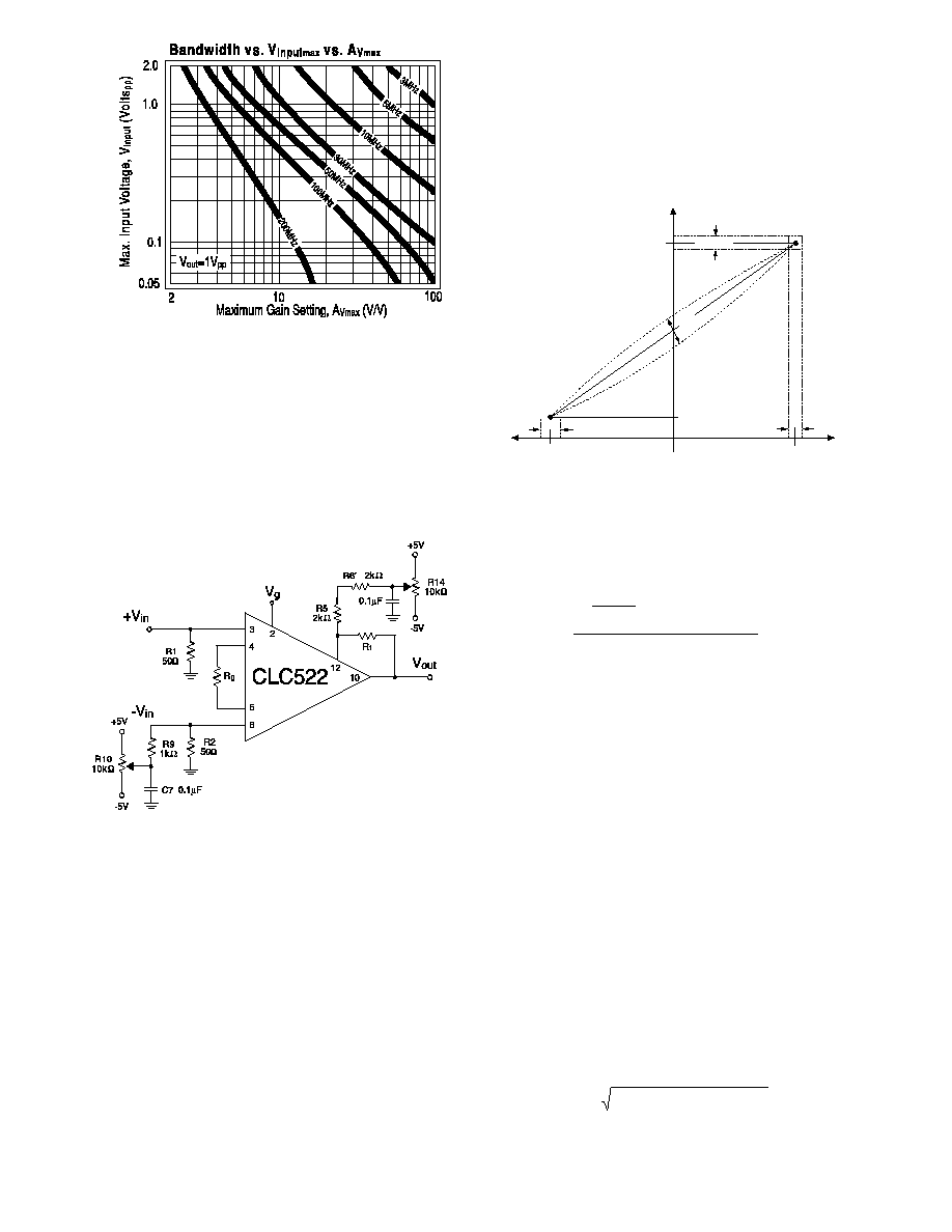
Fig. 2 illustrates the resulting CLC522 bandwidths as a
function of the maximum and minimum input voltages
when V
out
is held constant at 1V
pp
.
Adjusting Offsets
Treating the offsets introduced by the input and output
stages of the CLC522 is easily accomplished with a two
step process. The offset voltage of the output stage is
treated by first applying -1.1Volts on V
g,
which effectively
isolates the input stage and multiplier core from the
output stage. As illustrated in Fig. 3, the trim pot located
at R14 on the CLC522 Evaluation Board should then be
adjusted in order to null the offset voltage seen at the
CLC522's output (pin 10). Once this is accomplished, the
offset errors introduced by the input stage and multiplier
core can then be treated. The second step requires the
absence of an input signal and matched source imped-
ances on the two input pins in order to cancel the bias
current errors. This done then +1.1Volts should be
applied to V
g
and the trim pot located at R10 adjusted in
order to null the offset voltage seen at the CLC522's
output. If a more limited gain range is anticipated, the
above adjustments should be made at these operating
points.
Gain Errors
The CLC522's gain equation as theoretically expressed
in Eq. 2 must include the device's error terms in order to
yield the actual gain equation. Each of the gain error
Fig. 2
Fig. 3
terms are specified in the Electrical Characteristics table
and are defined below and illustrated in Fig. 4.
GACCU
: error of
A
V
max
,
expressed as ±dB.
GCNL
: deviation from theoretical expressed as ±%.
V
g
high
: voltage on V
g
producing
A
V
max
.
V
g
low
: voltage on V
g
producing A
Vmin
= 0V/V.
V
g
high
,
V
g
low
: error of V
g
high
,V
g
low
expresed as ±mV.
Combining these error terms with Eq. 2 gives the "gain
envelope" equation and is expressed in Eq. 7. From the
Electrical Characteristics table, the nominal endpoint
values of V
g
are: V
g
high
=+990mV and V
g
low
= -975mV.
Signal-Channel Nonlinearity
Signal-channel nonlinearity,
SGNL
, also known as integral
endpoint linearity, measures the non-linearity of an
amplifier's voltage transfer function. The CLC522's SGNL,
as it is specified in the Electrical Characteristics table, is
measured while the gain is set at its maximum (i.e.
V
g
=+1.1V). The Typical Performance Characteristics
plot labled "SGNL & Gain vs V
g
" illustrates the CLC522's
SGNL as V
g
is swept through its full range. As can be
seen in this plot, when the gain as reduced from
A
V
max
,
SGNL improves to < 0.02%(-74dB) at V
g
=0 and then
degrades somewhat at the lowest gains.
Noise
Fig. 5 describes the CLC522's input-refered spot noise
density as a function of
A
V
max
. The plot includes all the
noise contributing terms. At
A
V
max
= 10V/V, the CLC522
has a typical input-referred spot noise density (e
ni
) of
5.8nV/
Hz. The input
RMS
voltage noise can be deter-
mined from the following single-pole model:
Eq. 8
Further discussion and plots of noise and the noise model
is provided in Application Note OA-23. Comlinear also
provides SPICE models that model internal noise and
other parameters for a typical part.
A
V
max
A
V
A
V
min
V
g
low
V
g
high
V
g
±
GCNL
±
GACCU
±
V
g
high
±
V
g
low
Fig. 4
Eq . 7
A
A
V
V
V
V
V
V
V
V
GCNL
V
V
GACCU
g
g
g
g
g
g
g
g
low
low
high
high
low
low
=
-
±
(
)
±
-
±
(
)
± -
(
)
±
max
10
1
20
2
V
e
dB bandwidth
RMS
in
=
-
(
)
157
3
.
5
http://www.national.com