 | –≠–ª–µ–∫—Ç—Ä–æ–Ω–Ω—ã–π –∫–æ–º–ø–æ–Ω–µ–Ω—Ç: CLC532AJP | –°–∫–∞—á–∞—Ç—å:  PDF PDF  ZIP ZIP |
N
CLC532
High-Speed 2:1 Analog Multiplexer
General Description
The CLC532 is a high-speed 2:1 multiplexer with active input and
output stages. The CLC532 also employs a closed-loop design which
dramatically improves accuracy. This monolithic device is constructed
using an advanced high-performance bipolar process.
The CLC532 has been specifically designed to provide settling times
of 17ns to 0.01%. This, coupled with the adjustable noise-bandwidth,
makes the CLC532 an ideal choice for infrared and CCD imaging
systems. Channel-to-channel isolation is better than 80dB @
10MHz. Low distortion (80dBc) and spurious signal levels make the
CLC532 a very suitable choice for both I/Q processors and receivers.
The CLC532 is offered over both the industrial and military temperature
ranges. The Industrial versions, CLC532AJP\AJE\AID, are specified
from -40∞C to +85∞C and are packaged in 14-pin plastic DIP's, 14-pin
SOIC's and 14-pin Side-Brazed packages. The extended temperature
versions, CLC532A8B/A8D/A8L-2, are specified from -55∞C to +125∞C
and are packaged in a 14-pin hermetic DIP and 20-terminal LCC
packages. (Contact factory for LCC and CERDIP availability.)
Ordering Information ...
CLC532AJP
-40
o
C to +85
o
C
14-pin plastic DIP
CLC532AJE
-40
o
C to +85
o
C
14-pin plastic SOIC
CLC532ALC
-40
o
C to +85
o
C
dice
CLC532AMC
-55
o
C to +125
o
C
dice, MIL-STD-833
CLC532A8B
-55
o
C to +125
o
C
14-pin CERDIP;
MIL-STD-883
CLC532A8L-2A
-55
o
C to +125
o
C
20-terminal LCC;
MIL-STD-883
Contact factory for other packages and DESC SMD number.
June 1999
CLC532
High-Speed 2:1 Analog Multiplexer
Features
s
12-bit settling (0.01%) - 17ns
s
Low noise - 32
µ
Vrms
s
High isolation - 80dB @ 10MHz
s
Low distortion - 80dBc @ 5MHz
s
Adjustable bandwidth - 190MHz (max)
Applications
s
Infrared system multiplexing
s
CCD sensor signals
s
Radar I/Q switching
s
High definition video HDTV
s
Test and calibration
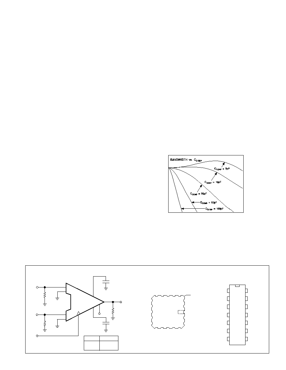
Typical Application
Pinout
DIP & SOIC
20-Terminal LCC
R
L
R
IN
R
IN
IN
B
10
6
IN
A
4
3
2
1
7
V
OUT
12
CHANNEL A
CHANNEL B
CHANNEL
SELECT
C
COMP2
C
COMP1
CLC532
D
REF
11
SELECT OUTPUT
1
Channel A
0
Channel B
GND
IN
A
GND
IN
B
DGND
D
REF
SELECT
+V
CC
+V
CC
COMP
1
OUTPUT
COMP
2
V
EE
V
EE
1
2
3
4
5
6
7
14
13
12
11
10
9
8
TOP VIEW
COMP
1
NC
OUTPUT
NC
COMP
2
14 15 16 17 18
9
10
11
12
13
8
7
6
5
4
3
2
1
20
19
D
REF
SELECT
NC
V
EE
V
EE
DGND
NC
IN
B
NC
GND
IN
A
GND
NC
+V
cc
+V
cc
INDEX CORNER
©
1999 National Semiconductor
Corporation
http://www.national.com
Printed in the U.S.A.
PARAMETER
1
CONDITIONS
TYP
MAX/MIN RATINGS
2
UNITS
SYMBOL
Case Temperature
CLC532AJP/AJE/AIB
+25
∞
C
-40
∞
C
+25
∞
C
+85
∞
C
FREQUENCY DOMAIN PERFORMANCE
-3dB bandwidth
V
OUT
<0.1Vpp
190
140
140
110
MHz
SSBW
-3dB bandwidth
V
OUT
=2Vpp
45
35
35
30
MHz
LSBW
gain flatness
V
OUT
<0.1Vpp
peaking
0.1MHz to 200MHz
0.2
0.7
0.7
0.8
dB
GFP
rolloff
0.1MHz to 100MHz
1.0
1.8
1.8
2.6
dB
GFR
linear phase deviation
dc to 100MHz
2.0
deg
LPD
differential gain
C
COMP
= 5pF; R
L
=150
0.05
%
DG
differential phase
C
COMP
= 5pF; R
L
=150
0.01
deg
DP
crosstalk rejection
2Vpp, 10MHz
80
75
75
74
dB
CT10
2Vpp, 20MHz
74
69
69
68
dB
CT20
2Vpp, 30MHz
68
63
63
62
dB
CT30
TIME DOMAIN PERFORMANCE
rise and fall time
0.5V step
2.7
3.3
3.3
3.8
ns
TRS
2V step
10
12.5
12.5
14.5
ns
TRL
settling time 2V step; from 50% V
OUT
±0.0025%
35
ns
TS14
±0.01%
17
24
24
27
ns
TSP
±0.1%
13
18
18
21
ns
TSS
overshoot
2.0V step
2
5
5
6
%
OS
slew rate
160
130
130
110
V/
µ
s
SR
SWITCH PERFORMANCE
channel to channel switching time
50% SELECT to 10%V
OUT
5
7
7
8
ns
SWT10
(2V step at output)
50% SELECT to 90%V
OUT
15
20
20
23
ns
SWT90
switching transient
30
mV
ST
DISTORTION AND NOISE PERFORMANCE
2nd harmonic distortion
2Vpp, 5MHz
80
67
67
67
dBc
HD2
3rd harmonic distortion
2Vpp, 5MHz
86
68
68
68
dBc
HD3
equivalent input noise
spot noise voltage
>1MHz
3.1
nV/
Hz
SNF
integrated noise
1MHz to 100MHz
32
42
42
46
µ
Vrms
INV
spot noise current
3
pA/
Hz
SNC
STATIC AND DC PERFORMANCE
* analog output offset voltage
1
6.5
3.5
5.5
mV
VOS
temperature coefficient
15
90
20
µ
V/∞C
DVIO
analog output offset voltage matching
TBD
mV
VOSM
* analog input bias current
50
250
120
120
µ
A
IBN
temperature coefficient
0.3
2.0
0.8
µ
A/∞C
DIBN
analog input bias current matching
TBD
µ
A
IBNM
analog input resistance
200
90
120
120
k
RIN
analog input capacitance
2
3.0
2.5
2.5
pF
CIN
* gain accuracy
±2V
0.998
0.988
0.988
0.988
V/V
GA
gain matching
±2V
TBD
V/V
GAM
integral endpoint non-linearity
±1V (full scale)
0.02
0.05
0.03
0.03
%FS
ILIN
output voltage
no load
±3.4
2.4
2.8
2.8
V
VO
output current
45
20
30
30
mA
IO
output resistance
dc
1.5
4.0
2.5
2.5
RO
DIGITAL INPUT PERFORMANCE
ECL mode (pin 6 floating)
input voltage logic HIGH
-1.1
-1.1
-1.1
V
VIH1
input voltage logic LOW
-1.5
-1.5
-1.5
V
VIL1
input current logic HIGH
14
50
30
30
µ
A
IIH1
input current logic LOW
50
270
110
110
µ
A
IIL1
TTL mode (pin 6 = +5V)
input voltage logic HIGH
2.0
2.0
2.0
V
VIH2
input voltage logic LOW
0.8
0.8
0.8
V
VIL2
input current logic HIGH
14
50
30
30
µ
A
IIH2
input current logic LOW
50
270
110
110
µ
A
IIL2
POWER REQUIREMENTS
* supply current (+V
CC
= +5.0V)
no load
23
30
28
25
mA
ICC
* supply current (-V
EE
= -5.2V)
no load
24
31
30
26
mA
IEE
nominal power dissipation
no load
240
mW
PD
* power supply rejection ratio
73
60
64
64
dB
PSRR
Min/max ratings are based on product characterization and simulation. Individual parameters are tested as noted. Outgoing quality levels are
determined from tested parameters.
Electrical Characteristics
(+V
CC
=+5.0V; -V
EE
=-5.2V; R
IN
=50
; R
L
=500
; C
COMP
=10pF; ECL Mode, pin 6 = NC)
http://www.national.com
2
Recommended Operating Conditions
Absolute Maximum Ratings
3
positive supply voltage (+V
CC
)
-0.5V to +7.0V
negative supply voltage (-V
EE
)
+0.5V to -7.0V
differential voltage between any two GND's
200mV
analog input voltage range
-V
EE
to +V
CC
digital input voltage range
-V
EE
to +V
CC
output short circuit duration (output shorted to GND)
Infinite
junction temperature
+150
∞
C
operating temperature range
CLC532AJP/AJE/AIB
-40
∞
C to +85
∞
C
storage temperature range
-65
∞
C to +150
∞
C
lead solder duration (+300
∞
C)
10 sec
ESD rating
<500V
transistor count
74
positive supply voltage (+V
CC
)
+5V
negative supply voltage (-V
EE
)
-5.2V or -5.0V
differential voltage between any two GND's
10mV
analog input voltage range
±2V
SELECT input voltage range (TTL mode)
0.0V to +3.0V
SELECT input voltage range (ECL mode)
-2.0V to 0.0V
C
COMP
range
2
0pF to 100pF
thermal data
JC
(∞C/W)
JA
(∞C/W)
14-pin plastic
55
100
14-pin Cerdip
35
85
14-pin SOIC
35
105
20-terminal LCC
35
50
Note 1:
Test levels are as follows:
*
AJ : 100% tested at +25∞C.
Note 2: The CLC532 does not require external C
COMP
capacitors for proper
operation.
Note 3: Absolute maximum ratings are limiting values, to be applied individually,
and beyond which the serviceability of the circuit may be impaired. Functional
operability under any of these conditions is not necessarily implied. Exposure to
maximum ratings for extended periods may affect device reliability.
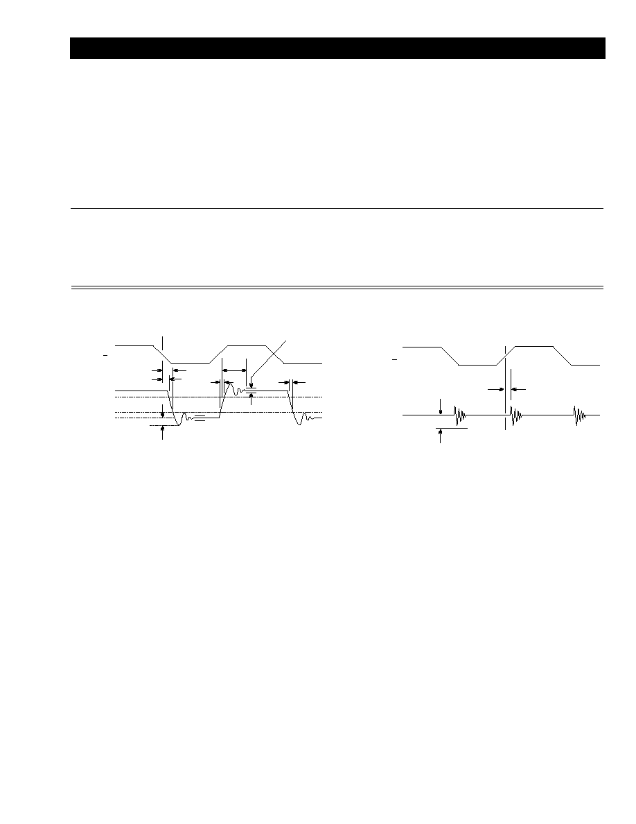
System Timing Diagram
Switching Transient Timing Diagram
A
SELECT
B
ST
2ns
~
~
OUTPUT
Channel A = 0V
Channel B = 0V
A
SELECT
B
SWT90
SWT10
90%
10%
TSx
TRx
TRx
SETTLING ERROR
WINDOW
CHANNEL A = +1V
CHANNEL B = -1V
OS
... where TSx is TS14 or TSP or TSS,
and TRx is TRS ro TSL.
OUTPUT
3
http://www.national.com
http://www.national.com
4
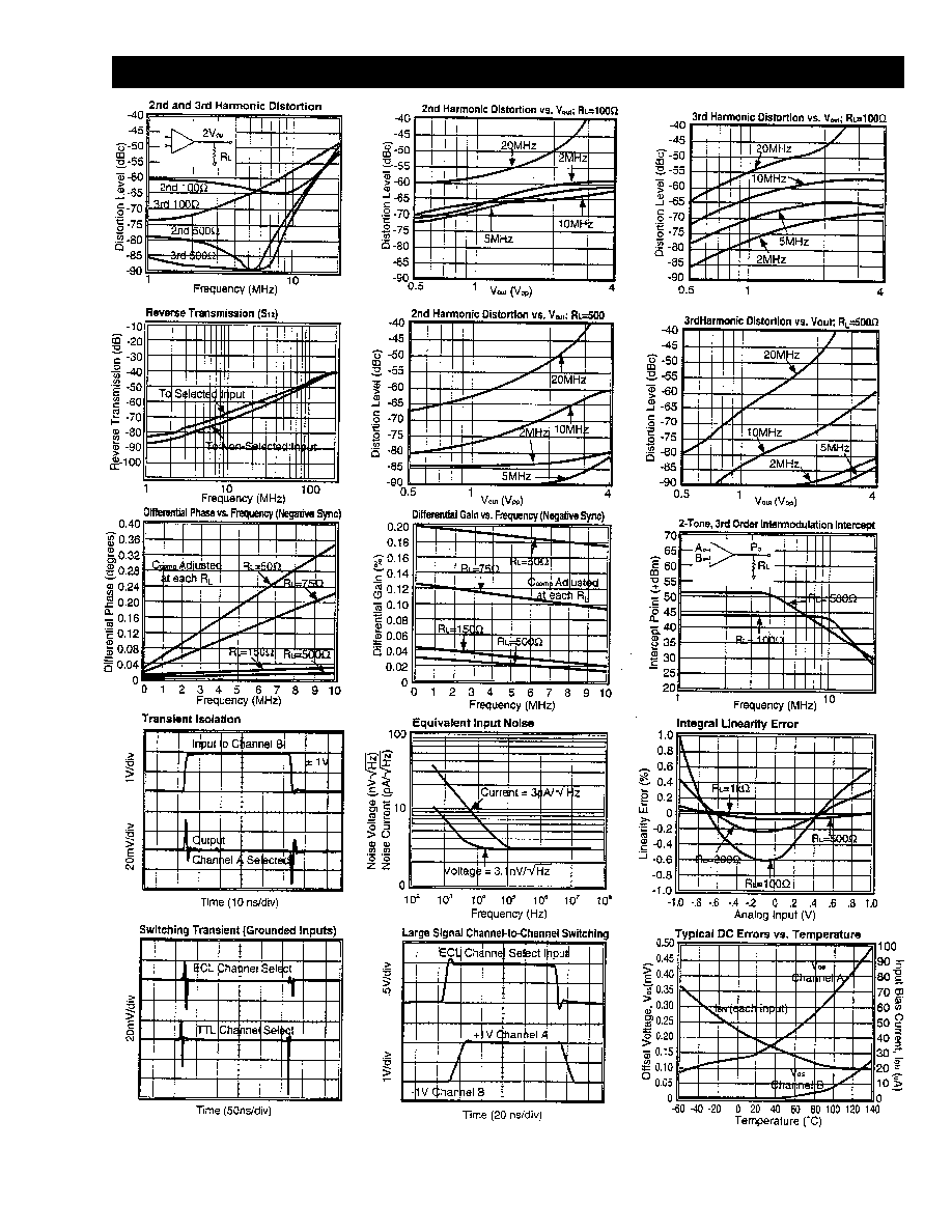
CLC532 Electrical Characteristics
(+25
∞
C unless specified)
5
http://www.national.com
CLC532 Electrical Characteristics
(+25
∞
C unless specified)