Features
s
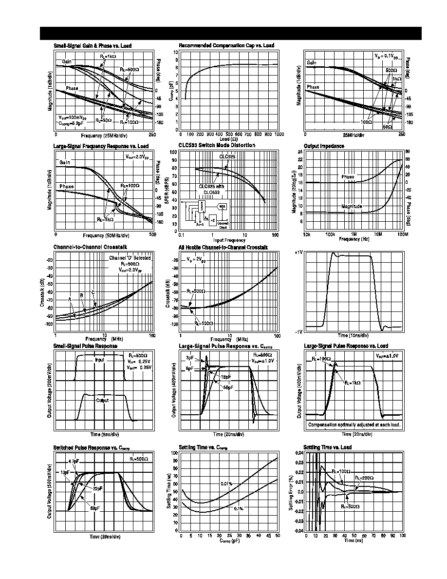
12-bit settling (0.01%) ≠ 17ns
s
Low noise ≠ 42
µ
Vrms
s
Isolation ≠ 80dB @ 10MHz
s
110MHz -3dB bandwidth (A
v
= +2)
s
Low distortion ≠ 80dB @ 5MHz
s
Adjustable bandwidth ≠ 180MHz (max)
Applications
s
Infrared system multiplexing
s
CCD sensor signals
s
Radar I/Q switching
s
High definition video HDTV
s
Test and calibration
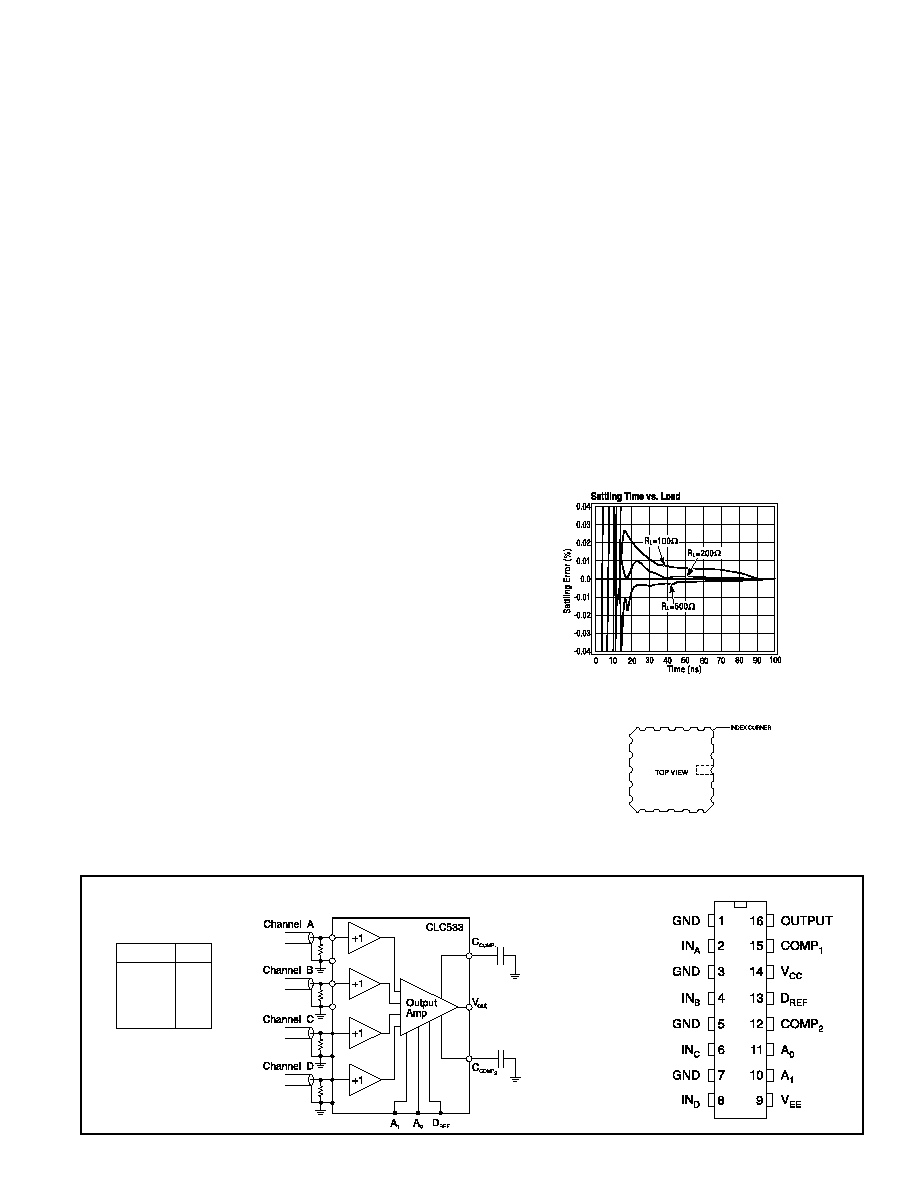
Functional Diagram
Pinout
DIP & SOIC
General Description
The CLC533 is a high-speed 4:1 multiplexer employing active
input and output stages. The CLC533 also employs a closed-loop
design which dramatically improves accuracy over conventional
analog multiplexer circuits. This monolithic device is constructed
using an advanced high-performance bipolar process.
The CLC533 has been specifically designed to provide a 24ns
settling time to 0.01%. This coupled with the adjustable band-
width, makes the CLC533 an ideal choice for infrared and CCD
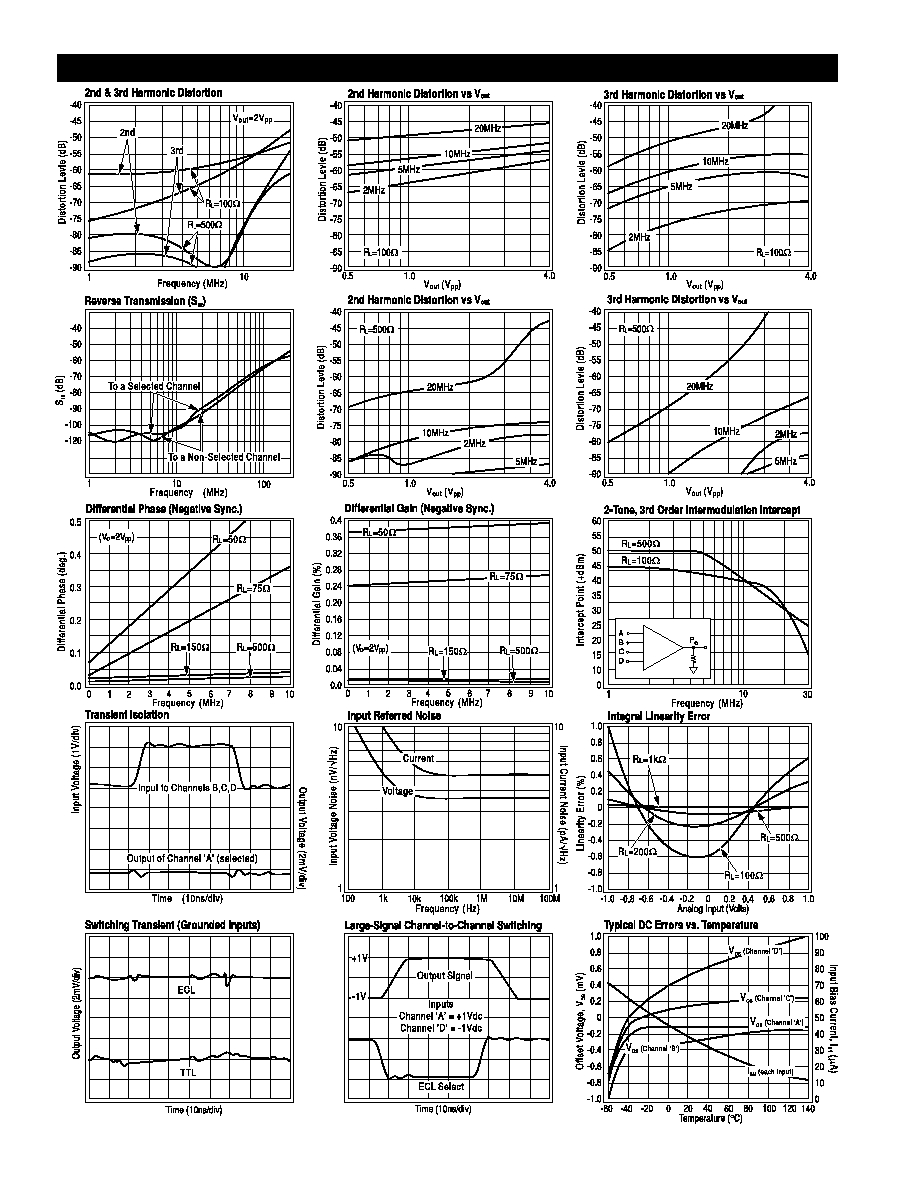
imaging systems, with channel-to-channel isolation of 80dB @
10MHz. Low distortion and spurious signal levels (-80dBc) make
the CLC533 a very suitable choice for I/Q processors in radar
receivers.
The CLC533 is offered over both the industrial and military tem-
perature ranges. The industrial versions, CLC533AJP\AJE\AIB,
are specified from -40∞C to +85∞C and are packaged in 16-pin
plastic DIPs, SOIC's and CERDIP packages. The extended tem-
perature versions, CLC533A8B/A8L-2A, are specified from -55∞C
to +125∞C and are packaged in 16-pin CERDIP and 20-terminal
LCC packages.
Ordering Information ...
CLC533AJP
-40∞C to +85∞C
16-pin plastic DIP
CLC533AJE
-40∞C to +85∞C
16-pin plastic SOIC
CLC533ALC
-40∞C to +85∞C
dice
CLC533A8B
-55∞C to +125∞C
16-pin CERDIP,
MIL-STD-883
CLC533AMC
-40∞C to +85∞C
dice, MIL-STD-833
CLC533A8L-2A
-55∞C to +125∞C
20-terminal LCC,
MIL-STD-883
Contact factory for other packages and DESC SMD number.
CLC533
High-Speed 4:1 Analog Multiplexer
N
June 1999
CLC533
High-Speed 4:1 Analog Multiple
x
er
A
1
A
0
OUT
0
0
A
0
1
B
1
0
C
1
1
D
ECL Mode - D
REF
= open
TTL Mode - D
REF
= +5V
IN
A
3
GND
2
NC
1
OUTPUT
20
COMP
1
19
GND
9
IN
D
10
NC 11
V
ee
12
A
1
13
14
A
0
15
COMP
2
16
NC
17
D
REF
18
V
cc
8
GND
7
IN
B
6
NC
5
GND
4
IN
c
© 1999 National Semiconductor Corporation
http://www.national.com
Printed in the U.S.A.
http://www.national.com
2
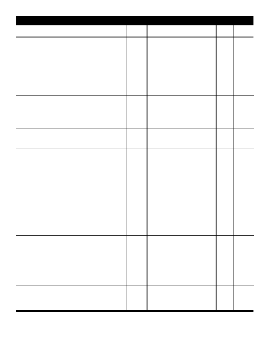
PARAMETERS
CONDITIONS
TYP
MIN/MAX RATINGS
2
UNITS SYMBOL
Ambient Temperature
CLC533AJP/AJE/AIB
+25∞C
-40∞C
+25∞C
+85∞C
FREQUENCY DOMAIN RESPONSE
-3dB bandwidth
V
OUT
< 0.1V
pp
180
130
130
110
MHz
SSBW
-3dB bandwidth
V
OUT
= 2V
pp
45
35
35
30
MHz
LSBW
gain flatness
V
OUT
< 0.1V
pp
peaking
0.1MHz to 200MHz
0.2
0.5
0.5
0.5
dB
GFP
rolloff
0.1MHz to 100MHz
1.0
2.0
2.0
3.0
dB
GFR
linear phase deviation
dc to 100MHz
2.0
deg
LPD
crosstalk rejection - 1 channel
2V
pp
, 10MHz
80
74
74
74
dB
CT10
2V
pp
, 20MHz
74
68
68
68
dB
CT20
2V
pp
, 30MHz
68
62
62
62
dB
CT30
crosstalk rejection - 3 channels
2V
pp
, 10MHz
80
74
74
74
dB
3CT10
2V
pp
, 20MHz
74
68
68
68
dB
3CT20
2V
pp
, 30MHz
68
62
62
62
dB
3CT30
TIME DOMAIN PERFORMANCE
rise and fall time
0.5V step
2.7
3.3
3.3
3.8
ns
TRS
2V step
10
12.5
12.5
14.5
ns
TRL
settling time
2
2V step
±0.01%
17
24
24
27
ns
TSP
±0.1%
13
18
18
21
ns
TSS
overshoot
2.0V step
2
5
5
6
%
OS
slew rate
160
130
130
110
V/
µ
s
SR
SWITCH PERFORMANCE
channel to channel switching time
50% SELECT to 10%V
OUT
6
8
8
9
ns
SWT10
(2V step at output)
50% SELECT to 90%V
OUT
16
21
21
24
ns
SWT90
switching transient
30
mV
ST
DISTORTION AND NOISE PERFORMANCE
2nd harmonic distortion
2V
pp
, 5MHz
80
67
67
67
dBc
HD2
3rd harmonic distortion
2V
pp
, 5MHz
86
67
67
67
dBc
HD3
equivalent input noise
spot noise voltage
> 1MHz
4.2
nV/
Hz
SNF
integrated noise
1MHz to 100MHz
42
54
51
mVrms
INV
spot noise current
5
pA/
Hz
SNF
STATIC AND DC PERFORMANCE
* analog output offset
1
12
3.5
4.5
mV
VOS
temperature coefficient
15
90
20
µ
V/∞C
DVIO
* analog input bias current
50
280
120
120
µ
A
IBN
temperature coefficient
0.3
2.0
0.8
µ
A/∞C
DIBN
analog input resistance
200
90
120
120
k
RIN
analog input capacitance
2
3.0
2.5
2.5
pF
CIN
* gain accuracy
±2V
0.994
0.988
0.988
0.988
V/V
GA
integral endpoint linearity
±1V (full scale)
0.02
0.05
0.03
0.03
%FS
ILIN
output voltage
no load
±3.4
2.4
2.8
2.8
V
VO
output current
45
20
50
50
mA
IO
output resistance
DC
1.5
4.0
2.5
2.5
RO
DIGITAL INPUT PERFORMANCE
ECL mode (D
REF
floating)
input voltage logic HIGH
-1.1
-1.1
-1.1
V
VIH1
input voltage logic LOW
-1.5
-1.5
-1.5
V
VIL1
input current logic HIGH
200
220
80
80
µ
A
IIH1
input current logic LOW
200
220
80
80
µ
A
IIL1
TTL mode (D
REF
= +5V)
input voltage logic HIGH
2.0
2.0
2.0
V
VIH2
input voltage logic LOW
0.8
0.8
0.8
V
VIL2
input current logic HIGH
200
220
80
80
µ
A
IIH2
input current logic LOW
200
220
80
80
µ
A
IIL2
POWER REQUIREMENTS
* supply current (+V
CC
= +5.0V)
no load
28
38
36
36
mA
ICC
* supply current (-V
ee
= -5.2V)
no load
28.5
39
37
37
mA
IEE
nominal power dissipation
no load
288
mW
PD
* power supply rejection ratio
-53
-60
-60
dB
PSRR
Min/max ratings are based on product characterization and simulation. Individual parameters are tested as noted. Outgoing quality levels are
determined from tested parameters.
CLC533 Electrical Characteristics
(+V
cc
= +5.0V; -V
ee
= -5.2V; R
in
= 50
; R
L
= 500
; C
COMP
= 8pf; ECL Mode, pin 13 = NC)
5
http://www.national.com
positive supply voltage (+V
cc
)
+5.0V
negative supply voltage (-V
ee
)
-5.2V
differential voltage between any two GND's
10mV
analog input voltage range
±2V
A
X
input voltage range (TTL mode)
0V to +5.0V
A
X
input voltage range (ECL mode)
0V to -2.0V
C
COMP
range
5pF to 100pF
thermal data
jc
(∞C/W)
ja
(∞C/W)
16-pin plastic
50
60
16-pin Cerdip
20
65
16-pin SOIC
60
75
20-terminal LCC
20
35
16-pin side brazed
20
50
positive supply voltage (+V
cc
)
-0.5V to +7.0V
negative supply voltage (-V
ee
)
+0.5V to -7.0V
differential voltage between any two GND's
200mV
analog input voltage range
-V
ee
to +V
cc
digital input voltage range
-V
ee
to +V
cc
output short circuit duration (shorted to GND)
Infinite
junction temperature
+150∞C
operating temperature range
CLC533AJP/AJE/AIB
-40∞C to +85∞C
storage temperature range
-65∞C to +150∞C
lead solder duration (+300∞C)
10 sec
ESD rating (human body model)
<500V
Recommended Operating Conditions
Absolute Maximum Ratings
3
Note 1: Test levels are as follows:
*
AJ : 100% tested at +25∞C.
Note 2: Settling time measured from the 50% analog output
transition.
Note 3: Absolute maximum ratings are limiting values, to be
applied individually, and beyond which the serviceability of the cir-
cuit may be impaired. Functional operability under any of these
conditions is not necessarily implied. Exposure to maximum rat-
ings for extended periods may affect device reliability.
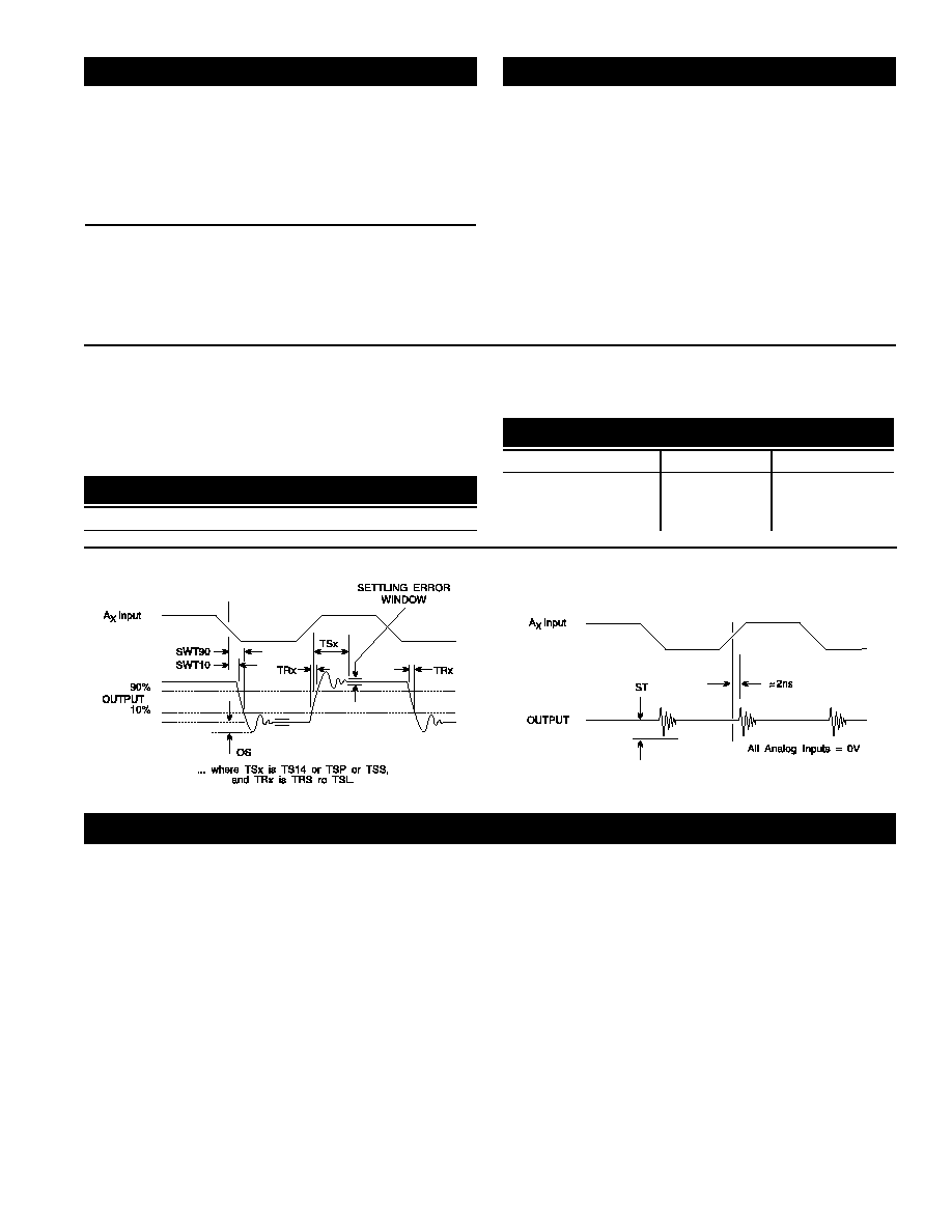
System Timing Diagram
Switching Transient Timing Diagram
APPLICATIONS INFORMATION
Operation
The CLC533 is a 4:1 analog multiplexer designed with a
closed loop architecture to provide very low harmonic
distortion and superior channel to channel isolation. This
low distortion, coupled with very fast switching
speed make the CLC533 an ideal multiplexer for data
conversion applications.
User selectable ECL or TTL
select logic adds to the versatility of this device. External
frequency response compensation allows the
performance of the CLC533 to be optimized for each
application.
Digital Interface and Channel Select
The CLC533 has two channel select pins which can be
used to select any one of the four inputs.
These
digital inputs can be configured to meet TTL, ECL or
CMOS logic levels with the D
REF
pin.
If D
REF
is left
open, then the A
0
and A
1
select inputs will respond to
ECL 10K switching levels (Figure 1). For TTL or CMOS
levels, D
REF
should be tied to V
cc
(Figure 2). There is an
internal series resistor which makes it possible to
connect D
REF
directly to the power supply. Select pins
according to the truth table shown on the front page. A
more positive voltage is considered to be a logic `1'.
Therefore with no connection to A
0
or A
1
the internal pull-
up resistors will select the D input to be passed through
to the output.
Compensation
The CLC533 is externally compensated, allowing
the user to select the bandwidth that best suits
the application. Decreasing bandwidth has two
advantages: lower noise and lower switching tran-
sients. In a sampled system, noise at frequencies
Package Thermal Resistance
Package
JC
JA
AJP
45∞C/W
95∞C/W
AJE
35∞C/W
100∞C/W
CERDIP
25∞C/W
65∞C/W
Reliability Information
Transistor count
144