CLC5506
Gain Trim Amplifier (GTA)
General Description
The CLC5506 is a low-noise amplifier with programmable
gain for use in cellular base stations, WLL, radar and RF/IF
subsystems where gain-control is required to increase the
dynamic range. The CLC5506 allows designers to compen-
sate for manufacturing component tolerances and tempera-
ture variations in receiver front ends. Maximum amplifier
gain is set at 26dB . A three-line MICROWIRE serial inter-
face allows 16dB of attenuation from the max gain setting in
precise 0.25dB steps.
The CLC5506 uses a differential input and output, allowing
large output swings on a single 5V rail. The differential output
is well suited for impedance matching networks driving SAW
filters or directly driving differential input analog to digital
converters (ADC). The differential output also makes it pos-
sible to drive transformers allowing designers the ability to
match a wide variety of transmission lines. The output ampli-
fier has excellent output drive with low distortion.
Digital control of the CLC5506 is accomplished using MI-
CROWIRE Interface. Data Out and a Load Enable are incor-
porated so that more than one CLC5506/channel may be
programmed per system.
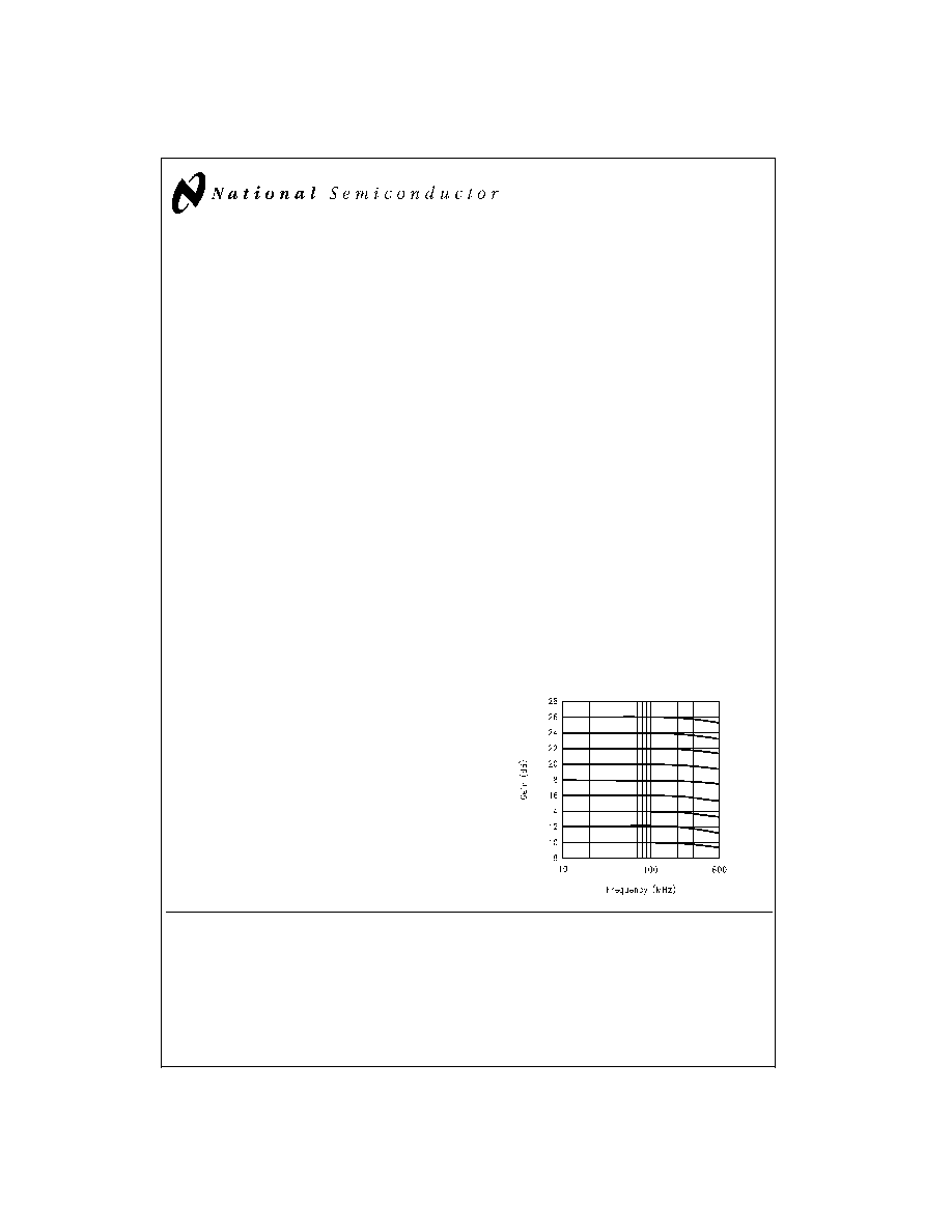
The CLC5506 maintains a 600MHz performance bandwidth
over its entire gain and attenuation range from +10dB to
+26dB. Gain control is divided into 64 equal steps of 0.25dB
and is dB-linear. Output drive and distortion performance are
excellent; In a 50
system, the third-order output intercept
point is +22dBm at nominal gain of 18dB at 25∞C. The
CLC5506 operates over the industrial temperature range of
-40∞C to +85∞C.
Features
n
600MHz bandwidth
n
26dB maximum gain
@
150MHz
n
16dB gain control range
n
Attenuation step size:
0.25dB
n
4.8dB noise figure
@
26dB
n
+22dBm output IP3
@
18dB gain
n
Digital
dB Linear
gain control
n
Supply voltage:
5V
n
Supply current:
75mA
n
Supply shutdown:
35µA
n
Package: SOIC-14
n
Typical at 25∞C
Applications
n
Cellular base-stations
n
Base station repeater
n
Wireless Local Loop
n
Radar
n
Receivers
n
IF amplifiers
n
Digital IF receiver
n
Software radio
n
Satellite communications
MICROWIRE
TM
Frequency Response vs. Gain Setting
DS101050-1
September 1999
CLC5506Gain
T
rim
Amplifier
(GT
A)
© 1999 National Semiconductor Corporation
DS101050
www.national.com
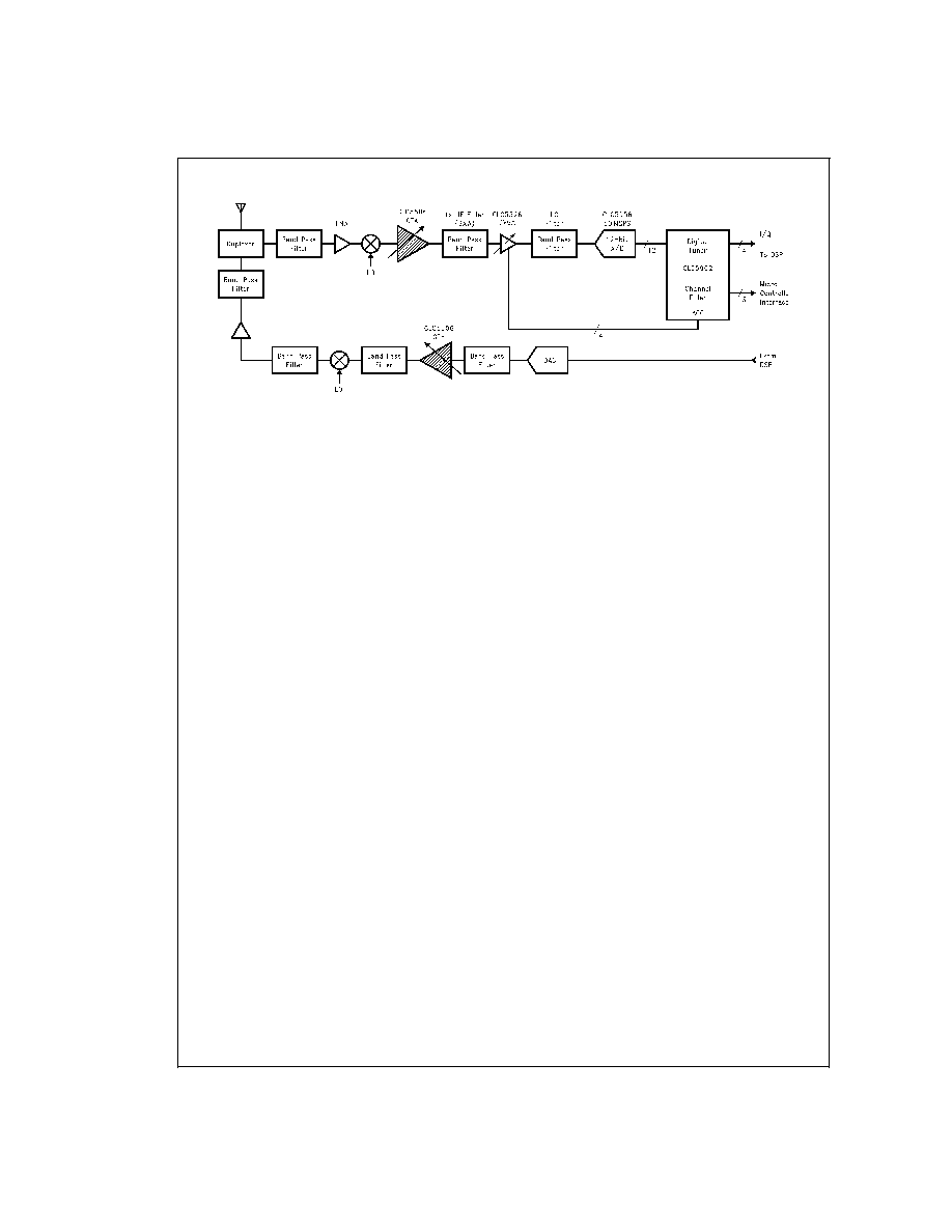
Typical Application
DS101050-2
www.national.com
2
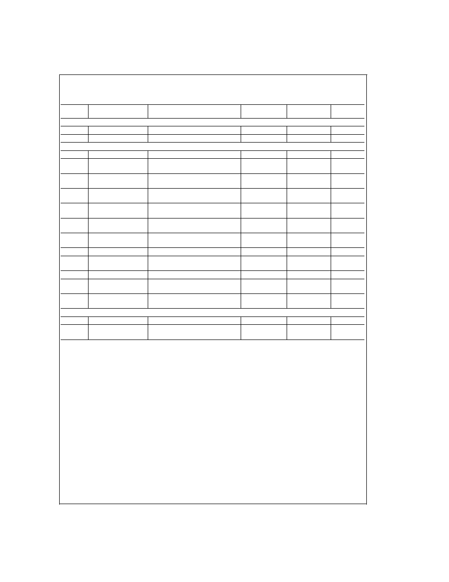
Connection Diagram
Pin #
Pin Name
Description
1
NC
No connection
2
GND
A
Analog ground
3
In+
Positive differential input
4
In-
Negative differential input
5
LE
MICROWIRE load enable input. High impedance CMOS input with Schmitt
trigger
6
Clock
MICROWIRE clock input. High impedance CMOS input with Schmitt trigger.
Data is clocked in on the rising edge of clock.
7
Data In
MICROWIRE data input. High impedance CMOS input with Schmitt trigger.
Binary serial data. Data entered Power Down first.
8
Data Out
MICROWIRE data output. High impedance CMOS input with Schmitt trigger.
9
GND
D
Digital ground
10
V
CCD
Digital supply voltage
11
Out-
Negative differential Output
12
Out+
Positive differential output
13
GND
A
Analog ground
14
V
CCA
Analog supply voltage
Ordering Information
Package
Temperature Range
Transport Media
NSC Drawing
-40∞C to +85∞C
SO-14
CLC5506IM
Rails
M14a
CLC5506IMX
2.5k Units Tape and
Reel
CLC5506PCASM
Fully loaded evaluation
board
CLC5506 Pin Diagram
DS101050-3
Top View
www.national.com
3
Absolute Maximum Ratings
(Note 1)
If Military/Aerospace specified devices are required,
please contact the National Semiconductor Sales Office/
Distributors for availability and specifications.
ESD tolerance(Note 2)
Human body model
2.5KV
Machine model
250V
Differential input voltage
+/-1V
Supply voltage
-0.3 to +6V
Digital input voltage
-0.3V to V
CC
Analog input voltage
-0.3V to V
CC
Output short circuit duration
Infinite
Lead temperature (soldering, 10
sec)
+300∞C
Storage temperature range
-65∞C to 150∞C
Junction temperature
155∞C
Differential voltage between any
two inputs
<
200mV
Operating Ratings
(Note 1)
Supply voltage (pins 10 and 14)
5V +/- 10%
Ambient temperature range
-40∞C to +85∞C
Junction Temperature Range
-40∞C to +150∞C
Package thermal resistance,
JA
127∞C/W
Electrical Characteristics
These conditions apply unless otherwise specified: T
J
= 25∞C, V
CCA
= V
CCD
= +5V: Gain = 25.75dB, R
Ldiff
= 100
, Pin =
-30dBm (Note 6),(Note 7).
Symbol
Parameter
Conditions
Typ
(Note 3)
Limit
(Note 4)
Units
Analog I/O
Frequency Response/Distortion/Noise
upper -3dB bandwidth
All Gain Codes
600
MHz
upper -1dB bandwidth
All Gain Codes
400
MHz
gain flatness in any
1MHz band
10MHz
<
f
<
600MHz, All Gain
Codes
0.003
dB
group delay
50MHz
<
f
<
600MHz
1.5
nsec
group delay ripple
50MHz
<
f
<
600MHz
0.5
nsec
output third order
intercept point
18dB Gain, f = 110MHz
22
dBm
noise figure
Gain = 25.75dB, (Note 6)
Gain = 18dB, (Note 6)
Gain = 10dB, (Note 6)
4.8
5.7
7.0
dB
dB
dB
1dB output
compression point
150MHz
4.0
dBm
2
nd
harmonic distortion
Pin = -30 dBm, fc = 200MHz
@
Gain = 25.75dB
@
Gain = 10dB
46
46
dBc
dBc
3
rd
harmonic distortion
Pin = -30 dBm, fc = 200MHz
@
Gain = 25.75dB
@
Gain = 10dB
49
56
dBc
dBc
Input/Output Isolation
power down mode
Full frequency band
45
dB
Gain Parameters: (Note 5)
maximum gain
Full temperature range
25.75
dB
minimum gain
Full temperature range
10
dB
gain step size
Full temperature range
0.25
dB
accuracy of gain
setting
@
25∞C
±
0.05
dB
gain variation over
temperature
Full temperature range
±
0.5
dB
Input/Output Characteristics:
input resistance
Differential
200
input capacitance
Differential
0.5
pF
www.national.com
4
Electrical Characteristics
(Continued)
These conditions apply unless otherwise specified: T
J
= 25∞C, V
CCA
= V
CCD
= +5V: Gain = 25.75dB, R
Ldiff
= 100
, Pin =
-30dBm (Note 6),(Note 7).
Symbol
Parameter
Conditions
Typ
(Note 3)
Limit
(Note 4)
Units
Input/Output Characteristics:
output resistance
Differential
5K
output capacitance
Differential
0.5
pF
Logic I/O
clock speed
Maximum
1
MHz
data to clock setup
time, T
CS
Minimum
50
nsec
data to clock hold
time, T
CH
Minimum
10
nsec
clock pulse width high,
T
CWH
Minimum
50
nsec
clock pulse width low,
T
CWL
Minimum
50
nsec
clock to load enable
setup time, T
ES
Minimum
50
nsec
high level input
voltage
0.7 V
CCD
V
low level input voltage
0.3 V
CCD
V
High level input
current
±
1.0
µA
low level input current
±
1.0
µA
high level output
voltage
Isource = 0.5mA
V
CCD
-0.8
V
low level output
voltage
Isink = 0.5mA
0.4
V
DC Characteristics:
Supply current
75
95
mA
Supply current in
power down mode
35
100
µA
Note 1: Absolute Maximum Ratings indicate limits beyond which damage to the device may occur. Operating Ratings indicate conditions for which the device is in-
tended to be functional, but specific performance is not guaranteed. For guaranteed specifications and the test conditions, see the Electrical Characteristics.
Note 2: Human body model, 1.5k
in series with 100pF. Machine model, 200
in series with 100pF.
Note 3: Typical values represent the most likely parametric norm.
Note 4: All limits are guaranteed by testing or statistical analysis, unless otherwise noted.
Note 5: AC test performed at 400MHz unless otherwise noted.
Note 6: Refer to test circuit schematic, loss of transformers is excluded from the measurement.
Note 7: Refer to test circuit schematic to see the definition of R
Ldiff
.
www.national.com
5