 | –≠–ª–µ–∫—Ç—Ä–æ–Ω–Ω—ã–π –∫–æ–º–ø–æ–Ω–µ–Ω—Ç: CLC5509CM | –°–∫–∞—á–∞—Ç—å:  PDF PDF  ZIP ZIP |
CLC5509
Ultra-Low Noise Preamplifier
General Description
The CLC5509 is a high performance, ultra-low noise pream-
plifier designed for applications requiring unconditional sta-
bility for wide ranges of complex input loads. Both input im-
pedance and gain are externally adjustable, which make it
simple to interface to peizoelectric ultrasound transducers.
The CLC5509 preamplifier's low 0.58nV
total input
noise makes it ideal for noise sensitive front ends. The high
repeatability in group delay over voltage and temperature
translates into precision edge measurements for Doppler ap-
plications.
The IC consists of an emitter input, common base amplifier
stage followed by a low distortion, closed loop buffer. Exter-
nal negative feedback creates a well controlled input imped-
ance to allow a near noiseless active input transmission line
termination. The preamp is stable against changes in source
impedance of 50 to 200
over temperature and supply
variations, with gains from 14dB to 26dB. The CLC5509
preamp architecture is also well suited for use with
magneto-resistive tape or disk drive heads. In these applica-
tions the head bias current can be reused to bias the
preamp. The part is packaged in an 8-pin plastic SOIC, and
runs off
±
5V supplies. External biasing is required for the in-
put signal path.
The CLC5509 is constructed using an advanced comple-
mentary bipolar process and National Semiconductor's
proven high performance architectures.
Features
n
0.58nV
total input noise
@
12MHz
n
<
.5ns group delay repeatability
n
High cutoff -3dB
@
33MHz
n
Low cutoff -3dB
@
0.5MHz
n
2.0dB noise figure
@
50
n
-60dBc intermod for 2V
PP
@
5MHz
n
Supply current: 11mA
n
Available in 8-pin SOIC
Applications
n
Ultrasound preamp
n
Tape drive preamp
n
Disk drive preamp
Connection Diagram
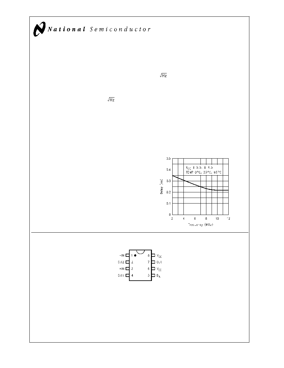
Group Delay Repeatability
DS101304-1
DS101304-3
Pinout
SOIC
January 2000
CLC5509
Ultra-Low
Noise
Preamplifier
© 2000 National Semiconductor Corporation
DS101304
www.national.com
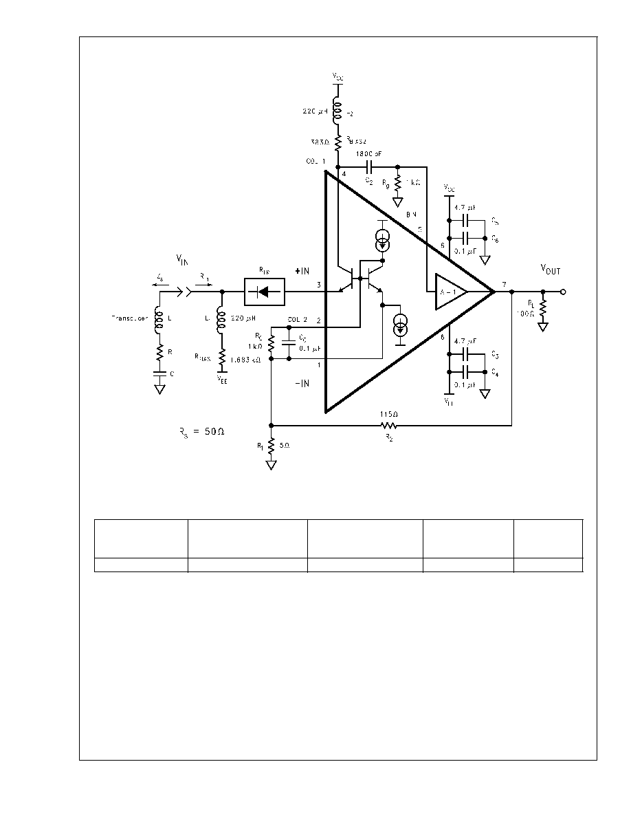
Typical Application
Ordering Information
Package
Temperature Range
Industrial
0∞C to 70∞C
Packaging
Marking
Transport Media
NSC
Drawing
8-pin SOIC
CLC5509CM
CLC5509CM
Rails
M08A
DS101304-2
Ultrasound PreAmp
CLC5509
www.national.com
2
Absolute Maximum Ratings
(Note 1)
If Military/Aerospace specified devices are required,
please contact the National Semiconductor Sales Office/
Distributors for availability and specifications.
Supply Voltage
±
5.5V
Output Current
70mA
Common-Mode Input Voltage
±
V
CC
Maximum Junction Temperature
+150∞C
Storage Temperature Range
-65∞C to +150∞C
Lead Temperature (soldering 10 sec)
+300∞C
ESD Rating (human body model)
4000V
Electrical Characteristics
(Note 3)
(V
CC
, V
EE
=
±
5V, R
S
= 50
, A
V
= 10V/V, R
g
= 1k
, R
L
= 100
; unless specified)
Symbol
Parameter
Conditions
Typ
Min/Max
Ratings
(Note 2)
Units
Ambient Temperature
CLC5509
+25∞C
+25∞C
Frequency Domain Response
-3dB Bandwidth
V
O
<
2.0V
PP
High Cutoff
-3dB
33
28
45
MHz
Low Cutoff
-3dB
0.5
0.4
0.7
MHz
Gain Flatness Inband
2
<
12.5MHz, V
O
<
1.0V
PP
-1.5
+.1
dB
Gain Accuracy
@
5MHz
±
0.3
dB
Phase Variation
3
<
9MHz, V
O
<
.1V
PP
1
Deg
Gain Variation
3
<
9MHz, V
O
<
.1V
PP
.3
dB
Time Domain Response
Rise and Fall Time
2V step
10
10
15
ns
Settling Time to 0.2%
2V step
1
µs
Overshoot
2V step
0
5
%
Group Delay
2.5MHz
<
10MHz, V
IN
= 10mV
PP
5.5
3
7.5
ns
Group Delay Repeatability
.5
ns
Distortion And Noise Response
2nd Harmonic Distortion
<
12.5MHz, V
IN
= 100mV
PP
-51
dBc
3rd Harmonic Distortion
-56
dBc
Intermodulation Distortion
@
5MHz
-65
dBc
Equivalent Input Noise Voltage (e
ni
)
>
1MHz, R
S
= 50
0.7
0.78
nV
Noise Figure
@
50
2
2.4
dB
Optimum R
S
85
80
110
Static, DC Performance
PSRR (preamp only)
<
1MHz
40
dB
Supply Current (preamp only)
R
L
=
9
11
mA
Miscellaneous Performance
Output Impedance
DC
<
12MHz
0.2
0.2
1
Output Voltage Range
R
L
= 100
±
2
±
1.7
V
Output Current
±
45
±
35
mA
CLC5509
www.national.com
3
Electrical Characteristics
(Note 3) (Continued)
Note 1: "Absolute Maximum Ratings" are those values beyond which the safety of the device cannot be guaranteed. They are not meant to imply that the devices
should be operated at these limits. The table of "Electrical Characteristics" specifies conditions of device operation.
Note 2: Min/max ratings are based on product characterization and simulation. Individual parameters are tested as noted. Outgoing quality levels are determined
from tested parameters.
Note 3: All data taken in circuit shown as typical application.
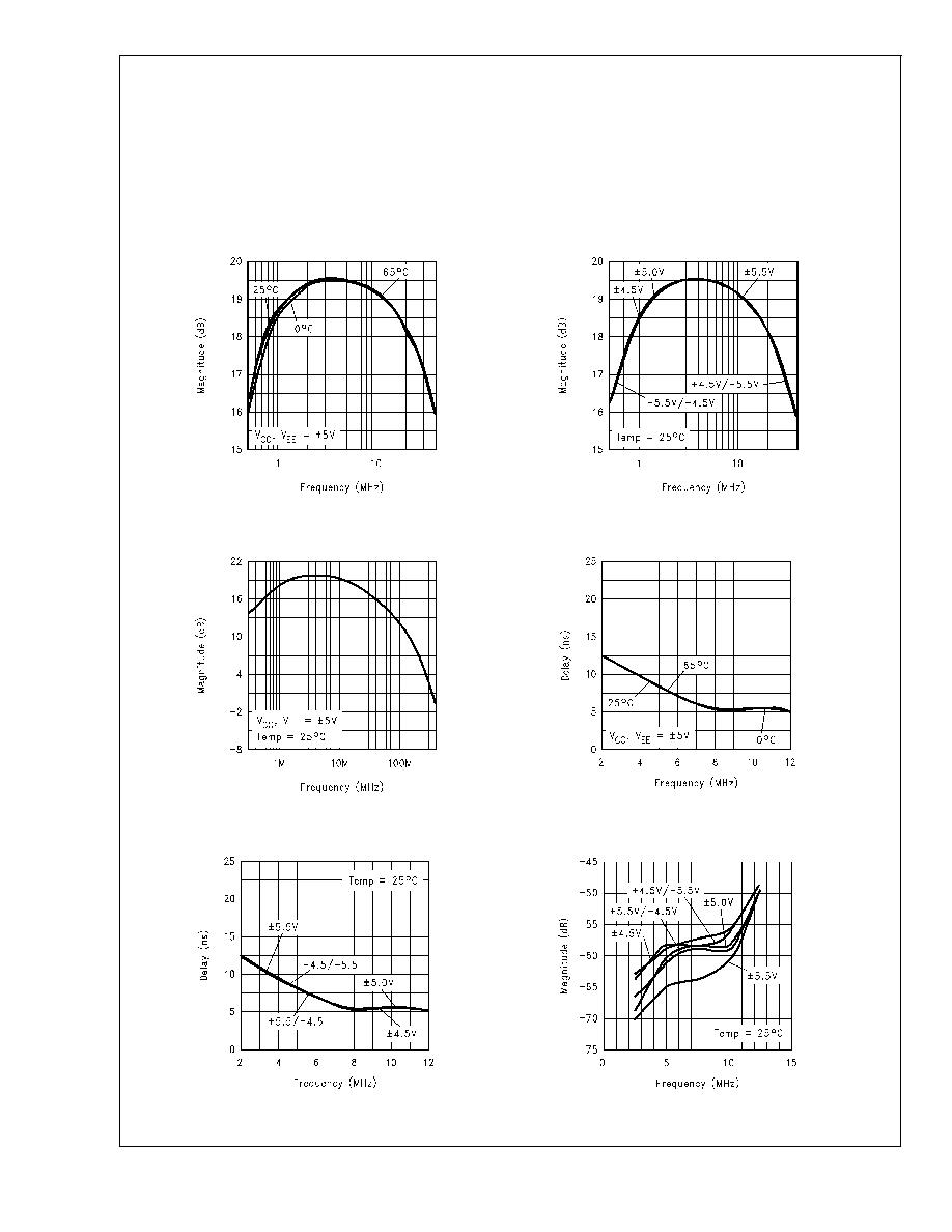
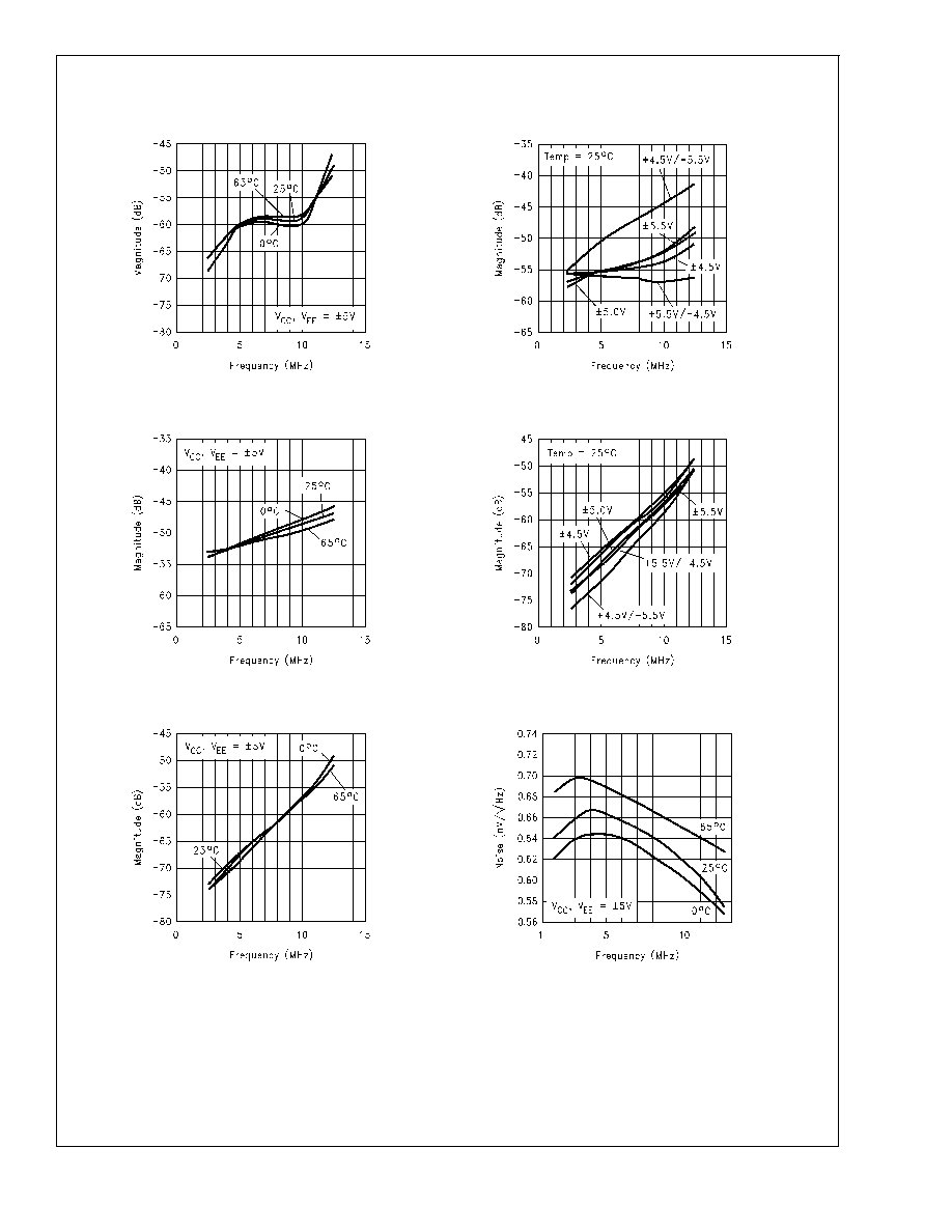
Typical Performance Characteristics
Frequency Response
DS101304-4
Frequency Response
DS101304-5
Frequency Response
DS101304-6
Group Delay
DS101304-7
Group Delay
DS101304-8
3rd Harmonic Distortion
DS101304-9
CLC5509
www.national.com
4
Typical Performance Characteristics
(Continued)
3rd Harmonic Distortion
DS101304-10
2rd Harmonic Distortion
DS101304-11
2rd Harmonic Distortion
DS101304-12
Intermodulation Distortion
DS101304-13
Intermodulation Distortion
DS101304-14
Total Input Referred Noise (R
S
= 50
)
DS101304-15
CLC5509
www.national.com
5