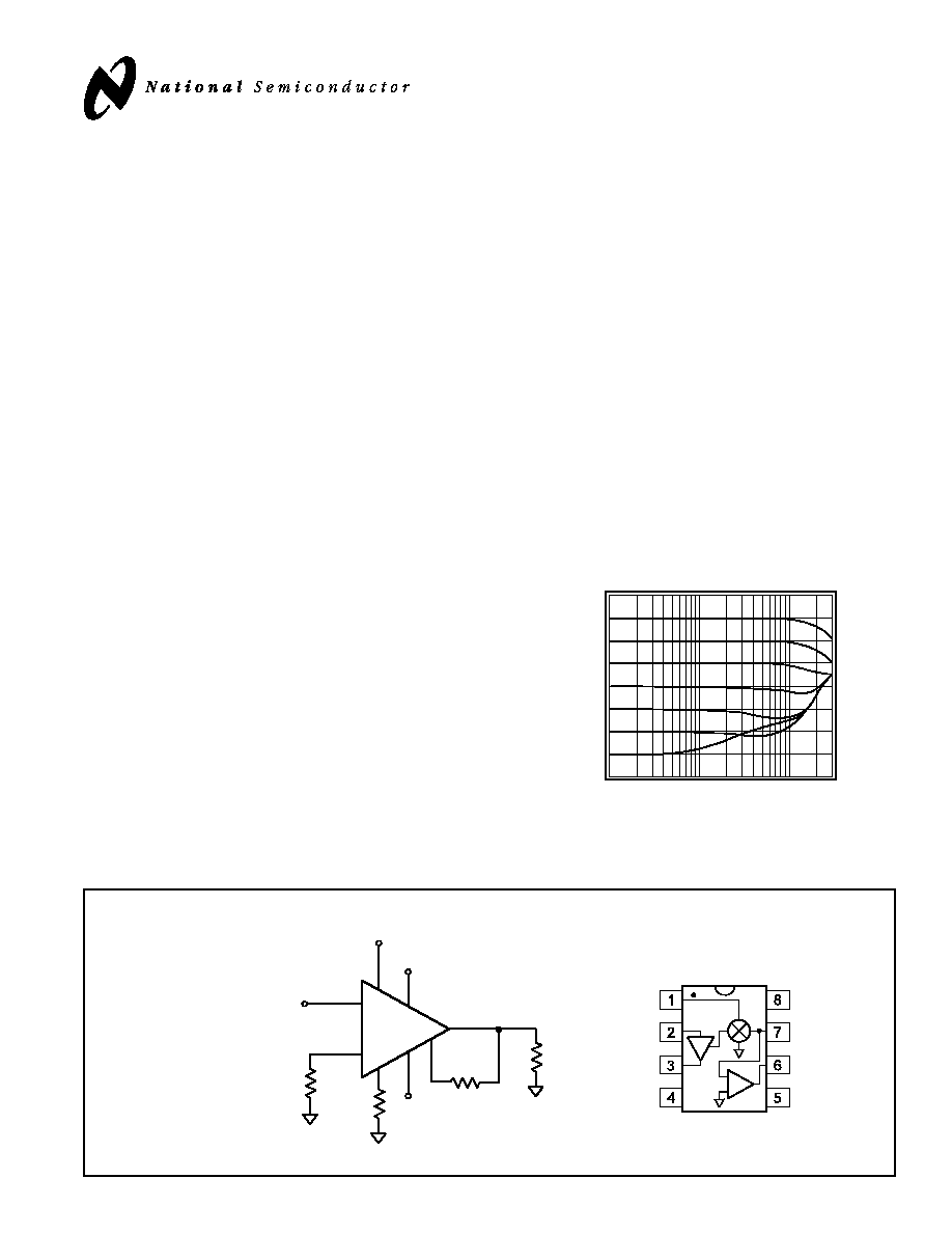
Typical Application
Variable Gain Amplifier
Circuit
CLC5523
Low-Power, Variable Gain Amplifier
March 2000
Features
s
Low power: 135mW
s
250MHz, -3dB bandwidth
s
Slew rate 1800V/
m
s
s
Gain flatness 0.2dB @ 75MHz
s
Rise & fall times 2.0ns
s
Low input voltage noise 4nV/
÷
Hz
Applications
s
Automatic gain control
s
Voltage controlled filters
s
Automatic signal leveling for A/D
s
Amplitude modulation
s
Variable gain transimpedance
General Descriptions
The CLC5523 is a low power, wideband, DC-coupled, voltage-
controlled gain amplifier. It provides a voltage-controlled gain
block coupled with a current feedback output amplifier. High
impedance inputs and minimum dependence of bandwidth on
gain make the CLC5523 easy to use in a wide range of
applications.
This amplifier is suitable as a continuous gain
control element in a variety of electronic systems which benefit
from a wide bandwidth of 250MHz and high slew rate of
1800V/
m
s, with only 135mW of power dissipation.
Input impedances in the megaohm range on both the signal
and gain control inputs simplify driving the CLC5523 in any
application. The CLC5523 can be configured to use pin 3 as a
low impedance input making it an ideal interface for current
inputs. By using the CLC5523's inverting configuration in which
R
G
is driven directly, inputs which exceed the device's input
voltage range may be used.
The gain control input (V
G
), with a 0 to 2V input range, and a
linear-in-dB gain control, simplifies the implementation of AGC
circuits. The gain control circuit can adjust the gain as fast as
4dB/ns. Maximum gains from 2 to 100 are accurately and simply
set by two external resistors while attenuation of up to 80dB from
this gain can be achieved.
The extremely high slew rate of 1800V/
m
s and wide bandwidth
provides high speed rise and fall times of 2.0ns, with settling time
for a 2 volt step of only 22ns to 0.2%. In time domain applications
where linear phase is important with gain adjust, the internal cur-
rent mode circuitry maintains low deviation of delay over a wide
gain adjust range.
Frequency Response with Changes in V
g
Magnitude (10dB/div)
Frequency (Hz)
30
20
10
0
-10
-20
-30
-40
-50
1M
10M
100M
CLC5523
Lo
w-P
o
wer
,
V
ariab
le Gain Amplifier
© 2000 National Semiconductor Corporation
http://www.national.com
Printed in the U.S.A.
+
-
CLC5523
R
f
V
o
V
in
R
g
2
3
4
1
V
G
R
L
5
-5V
8
+5V
6
7
25
W
V
G
V
IN
R
g
GND
I-
V
O
-V
CC
+V
CC
+
-
X1
Pinout
DIP & SOIC
http://www.national.com
2
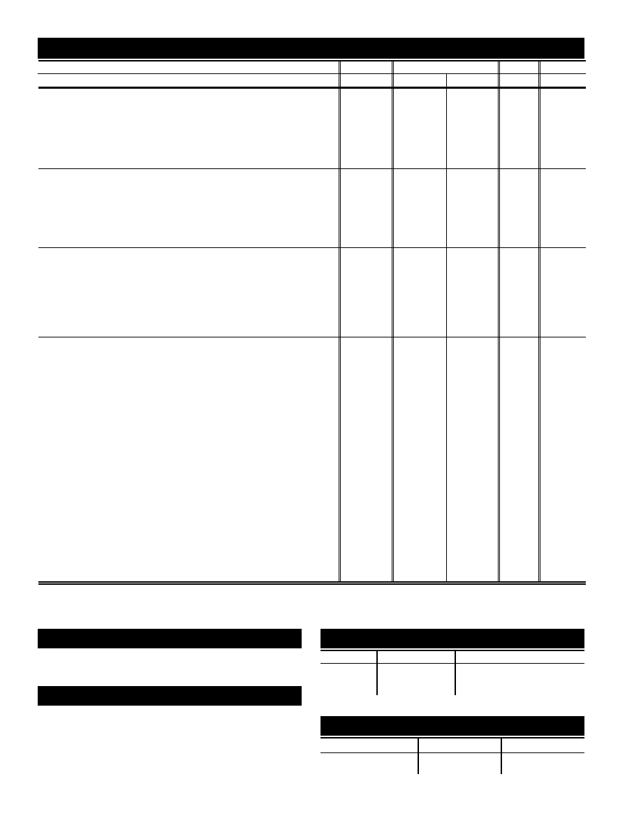
CLC5523 Electrical Characteristics
(V
CC
= ±5V, R
f
= 1k, R
g
= 100
W
, R
L
= 100
W
, V
G
= 2V
;
unless specified)
PARAMETERS
CONDITIONS
TYP
MIN/MAX RATINGS
UNITS
NOTES
Ambient Temperature
CLC5523I
+25∞C
25∞C
-40 to 85∞C
FREQUENCY DOMAIN RESPONSE
-3dB bandwidth
V
o
< 0.5V
pp
250
150
125
MHz
V
o
< 4.0V
pp
100
45
35
MHz
peaking
DC to 200MHz (V
o
= 0.5V
pp
)
0
0.8
2.0
dB
rolloff
DC to 75MHz (V
o
= 0.5V
pp
)
0.2
1.0
1.2
dB
linear phase deviation
DC to 75MHz (V
o
= 0.5V
pp
)
0.6
1.5
3.0
deg
gain control bandwidth
V
in
= 0.2V
DC
, V
g
= 1V
DC
95
70
60
MHz
TIME DOMAIN RESPONSE
rise and fall time
0.5V step
2.0
2.8
3.0
ns
overshoot
0.5V step
6.0
15
20
%
settling time to 0.2%
2V step
22
30
60
ns
non-inverting slew rate
4V step
700
450
400
V/
m
s
inverting slew rate
4V step
1800
1000
700
V/
m
s
gain control response rate
4
dB/nS
1
DISTORTION AND NOISE RESPONSE
2
nd
harmonic distortion
1V
pp
, 5MHz
-65
≠
≠
dBc
3
rd
harmonic distortion
1V
pp
, 5MHz
-80
≠
≠
dBc
2
nd
harmonic distortion
1V
pp
, 10MHz
-57
-52
-40
dBc
3
rd
harmonic distortion
1V
pp
, 10MHz
-75
-58
-54
dBc
input referred total noise
V
g
= 2V
5
6
7
nV/
÷
Hz
input referred voltage noise
4
5.5
5.5
nV/
÷
Hz
R
g
referred current noise
36
50
60
pA/
÷
Hz
STATIC DC PERFORMANCE
output offset voltage
50
120
150
mV
A
V
in
signal input
input voltage range
R
g
open
±3.8
±3.6
±3.3
V
input bias current
3.0
8.0
16
m
A
A
input resistance
3.0
1.0
0.8
M
W
input capacitance
1.0
1.5
1.7
pF
I
R
g
max
0∞ to 70∞C
7.0
5.0
4.0
mA
I
R
g
max
-40∞ to 85∞C
7.0
5.0
2.5
mA
signal ch. non-linearity SGNL V
o
= 2V
pp
0.04
0.1
0.2
%
gain accuracy*
0.3
0.5
0.9
dB
A
V
g
gain input
input bias current
0.5
2.0
4.0
m
A
input resistance
10
2.0
2.0
M
W
input capacitance
1.0
1.5
1.5
pF
ground pin current
40
55
65
m
A
power supply rejection ratio
input-referred
57
50
46
dB
supply current
R
L
=
•
13.5
15
16
mA
A
output voltage range
no load
±3.4
±3.0
±2.3
V
output voltage range
R
L
= 100
W
±3.0
±2.5
±2.3
V
output impedance
0.1
0.15
0.15
W
output current
80
65
50
mA
transistor count
146
*maximum gain is defined as R
f
/R
g
Min/max ratings are based on product characterization and simulation. Individual parameters are tested as noted. Outgoing quality levels are
determined from tested parameters.
Absolute Maximum Ratings
supply voltage
±7V
output current
±80mA
maximum junction temperature
+150∞C
storage temperature range
-65∞C to +150∞C
lead temperature (soldering 10 sec)
+300∞C
ESD rating (human body model)
TBD
Notes
A) I-level: spec is 100% tested at +25∞C.
1) See plot
"Gain Control Settling Time".
Ordering Information
Model
Temp Range
Description
CLC5523IN
-40∞C to +85∞C
8-pin DIP
CLC5523IM
-40∞C to +85∞C
8-pin Small outline
CLC5523IMX
-40∞C to +85∞C
8-pin Small outline tape and reel
Contact the factory for other packages.
Package Thermal Resistance
Package
q
JC
q
JA
DIP (IN)
65∞C/W
115∞C/W
Small Outline (IM)
55∞C/W
135∞C/W
5
http://www.national.com
The key features of the CLC5523 are:
s
Low Power
s
Broad voltage controlled gain and attenuation
range
s
Bandwidth independent, resistor programmable
gain range
s
Broad signal and gain control bandwidths
s
Frequency response may be adjusted with R
f
s
High Impedance signal and gain control Inputs
The CLC5523 combines a closed loop input buffer, a volt-
age controlled variable gain cell and an output amplifier.
The input buffer is a transconductance stage whose gain
is set by the gain setting resistor, R
g
. The output amplifi-
er is a current feedback op amp and is configured as a
transimpedance stage whose gain is set by, and equal to,
the feedback resistor, R
f
. The maximum gain, A
vmax
, of
the CLC5523 is defined by the ratio; R
f
/ R
g
.
As the
gain control input (V
G
) is adjusted over its 0 to 2V range,
the gain is adjusted over a range of 80dB relative to the
maximum set gain.
Setting the CLC5523 Maximum Gain
Although the CLC5523 is specified at A
vmax
= 10, the
recommended A
vmax
varies between 2 and 100. Higher
gains are possible but usually impractical due to
output offsets, noise and distortion. When varying A
vmax
several tradeoffs are made:
R
g
: determines the input voltage range
R
f
: determines overall bandwidth
The amount of current which the input buffer can source
into R
g
is limited and is specified in the I
Rgmax
spec. This
sets the maximum input voltage:
The effects of maximum input range on harmonic distortion
are illustrated in the
Input Harmonic Distortion plot.
Variations in R
g
will also have an effect on the small
signal bandwidth due to its loading of the input buffer and
can be seen in
Frequency Response vs. R
g
. Changes in
R
f
will have a more dramatic effect on the small signal
bandwidth. The output amplifier of the CLC5523 is a
current feedback amplifier(CFA) and its bandwidth is
determined by R
f
. As with any CFA, doubling the feed-
back resistor will roughly cut the bandwidth of the device
in half (refer to the plot
Frequency Response vs. R
f
). For
more information covering CFA's, there is
a basic tutorial, OA-20,
Current Feedback Myths
Debunked or a more rigorous analysis, OA-13, Current
Feedback Amplifier Loop Gain Analysis and Performance
Enhancements.
Using the CLC5523 in AGC Applications
In AGC applications, the control loop forces the CLC5523
to have a fixed output amplitude. The input amplitude will
vary over a wide range and this can be the issue that
limits dynamic range.
At high input amplitudes, the
distortion due to the input buffer driving R
g
may exceed
that which is produced by the output amplifier driving the
load. In the plot,
Harmonic Distortion vs. Gain, second
and third harmonic distortion are plotted over a gain
range of nearly 40dB for a fixed output amplitude
of 100mV
pp
in the specified configuration, R
f
= 1k,
R
g
= 100
W
. When the gain is adjusted to 0.1 (i.e. 40dB
down from A
vmax
), the input amplitude would be 1V
pp
and
we can see the distortion is at its worst at this gain. If the
output amplitude of the AGC were to be raised above
100mV, the input amplitudes for gains 40dB down from
A
vmax
would be even higher and the distortion would
degrade further. It is for this reason that we recommend
lower output amplitudes if wide gain ranges are desired.
Using a post-amp like the CLC404 or CLC409 would be
the best way to preserve dynamic range and yield output
amplitudes much higher than 100mV
pp
.
Another way of addressing distortion performance and
its limitations on dynamic range, would be to raise the
value of R
g
. Just like any other high-speed amplifier, by
increasing the load resistance, and therefore decreasing
the demanded load current, the distortion performance
will be improved in most cases. With an increased R
g
, R
f
will also have to be increased to keep the same A
vmax
and this will decrease the overall bandwidth.
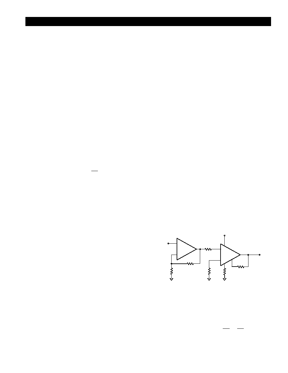
Gain Partitioning
If high levels of gain are needed, gain partitioning should
be considered.
Figure 1: Gain Partitioning
The maximum gain range for this circuit is given by the
following equation:
CLC5523 Operation
A
R
R
vmax
f
g
=
V (max)
I
R
in
R max
g
g
=
◊
CLC5523
R
f
R
g
2
3
4
1
V
G
6
7
25
W
+
-
CLC425
V
in
R
1
R
2
25
Wz
R
c
V
o
maximum gain
1
R
R
R
R
2
1
f
g
=
+
Ê
Ë
Á
ˆ
¯
˜ ◊
Ê
Ë
Á
ˆ
¯
˜