CLC5526
Digital Variable Gain Amplifier (DVGA)
General Description
The CLC5526 is a high performance, digitally controlled,
variable-gain amplifier (DVGA). It has been designed for use
in a broad range of mixed signal and digital communication
applications such as mobile radio, cellular base stations and
back-channel modems where automatic-gain-control (AGC)
is required to increase system dynamic range.
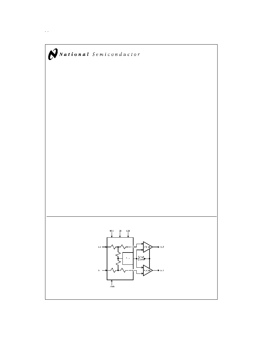
The CLC5526 has differential input and output, allowing
large signal swings on a single 5V rail. The input impedance
is 200
. The differential output impedance is 600
and is
designed to drive a 1 k
differential load. The output ampli-
fier
has
excellent
intermodulation
performance.
The
CLC5526 is designed to accept signals from RF elements
and maintain a terminated impedance environment.
The CLC5526 maintains a 350 MHz bandwidth over its en-
tire gain and attenuation range from +30 dB to -12 dB. Inter-
nal clamping ensures very fast overdrive recovery. Two tone
intermodulation distortion is excellent: at 150 MHz, 1 V
pp
it is
-64 dBc.
Input signals to the CLC5526 are scaled by an accurate, dif-
ferential R-2R resistive ladder with an input impedance of
200
. A scaled version of the input is selected under digital
control and passed to the internal amplifier. The input com-
mon mode level is set at 2.4V via a bandgap referenced bias
generator which can be overridden by an external input.
Following the resistive ladder is a fixed, 30 dB gain amplifier.
The output stage common mode voltage of the CLC5526 is
set to 3V, by internal, positive supply connected resistors.
Digital control of the CLC5526 is accomplished by a 3-bit
parallel gain control input and a data valid pin to latch the
data. If the data is not latched, the DVGA is transparent to
gain control updates. All digital inputs are TTL/CMOS com-
patible.
A shutdown input reduces the CLC5526 supply currrent to a
few mA. During shutdown, the input termination is main-
tained and current attenuation settings are held.
The CLC5526 operates over the industrial temperature
range of -40�C to +85�C. The part is available in a 20-pin
SSOP package.
Features
n
350 MHz bandwidth
n
Differential input and output
n
Gain control: parallel w/data latching
n
Supply voltage:
+5V
n
Supply current:
48 mA
Key Specifications
n
Low two tone intermod:
distortion: -64 dBc
@
1 V
PP
, 150 MHz
24.5 dBm IP3, 150 MHz
n
Low noise:
2.5 nV/
Hz (max gain),
9.3 dB noise figure (max gain)
n
Wide gain range:
+30 dB to -12 dB
n
Gain step size:
6 dB
Applications
n
Cellular/PCS base stations
n
IF sampling receivers
n
Infrared/CCD imaging
n
Back-channel modems
n
Electro-optics
n
Instrumentation
n
Medical imaging
n
High definition video
Block Diagram
DS015016-2
June 1999
CLC5526
Digital
V
ariable
Gain
Amplifier
(DVGA)
� 1999 National Semiconductor Corporation
DS015016
www.national.com
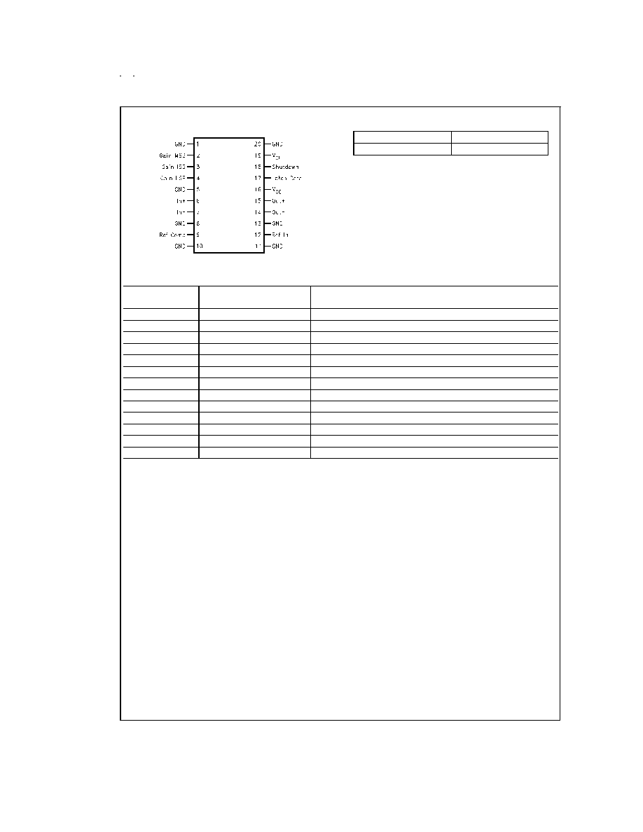
Pin Configuration
Ordering Information
CLC5526MSA
20-Pin SSOP
CLC5526PCASM
Evaluation Board
Pin Descriptions
Pin
Name
Pin
No.
Description
GND
1, 5, 8, 10, 11, 13, 20
Circuit ground.
Gain MSB
2
Gain Selection Most Significant Bit
Gain ISB
3
Gain Selection Data Bit
Gain LSB
4
Gain Selection Least Significant Bit
In+
6
Positive Differential Input
In-
7
Negative Differential Input
Ref Comp
9
Reference Compensation
V
CC
16, 19
Positive Supply Voltage
Shutdown
18
Low Power Standby Control (Active High)
Latch Data
17
Data Latch Control (Active High)
Out+
15
Positive Differential Output
Out-
14
Negative Differential Output
Ref In
12
External Reference Input
DS015016-1
www.national.com
2
Absolute Maximum Ratings
(Note 1)
If Military/Aerospace specified devices are required,
please contact the National Semiconductor Sales Office/
Distributors for availability and specifications.
Positive Supply Voltage (V
CC
)
-0.5V to +6V
Differential Voltage between any
Two Grounds
<
200 mV
Analog Input Voltage Range
-0.5V to +V
CC
Digital Input Voltage Range
-0.5V to +V
CC
Output Short Circuit Duration
(one-pin to ground)
Infinite
Junction Temperature
175�C
Storage Temperature Range
-65�C to +150�C
Lead Solder Duration (+300�C)
10 sec
Recommended Operating
Conditions
Positive Supply Voltage (V
CC
)
+5V
�
5%
Differential Voltage between any
Two Grounds
<
10 mV
Analog Input Voltage Range, AC
Coupled
�
0.5V
Operating Temperature Range
-40�C to +85�C
Package Thermal Resistance
Package
JA
JC
20-Pin SSOP
90�C/W
38�C/W
Reliability Information
Transistor Count
300
Electrical Characteristics
The following specifications apply for V
CC
= +5V, R
L
= 1 k
maximum gain setting. Boldface limits apply for T
A
= T
min
=
-40�C to T
max
= +85�C, all other limits T
A
= 25�C (Notes 2, 3, 4).
Symbol
Parameter
Conditions
Min
Typ
Max
Units
DYNAMIC PERFORMANCE
BW
Small-Signal Bandwidth
350
MHz
NOISE AND DISTORTION
2nd Harmonic Distortion
f
IN
= 150 MHz, 1 V
PP
53
67
dBc
f
IN
= 250 MHz, 1 V
PP
64
dBc
f
IN
= 150 MHz, 2 V
PP
43
62
dBc
f
IN
= 250 MHz, 2 V
PP
58
dBc
3rd Harmonic Distortion
f
IN
= 150 MHz, 1 V
PP
53
71
dBc
f
IN
= 250 MHz, 1 V
PP
70
dBc
f
IN
= 150 MHz, 2 V
PP
43
57
dBc
f
IN
= 250 MHz, 2 V
PP
56
dBc
IMD
Two Tone Intermodulation
Distortion
f
1
= 149.9 MHz, f
2
= 150.1 MHz,
1 V
PP
Composite
64
dBc
f
1
= 149.9 MHz, f
2
= 150.1 MHz,
2 V
PP
Composite
61
dBc
f
1
= 249.9 MHz, f
2
= 250.1 MHz,
1 V
PP
Composite
63
dBc
f
1
= 249.9 MHz, f
2
= 250.1 MHz,
2 V
PP
Composite
54
dBc
Two Tone, 3rd Order
Intermodulation
150 MHz
24.5
dBm
Thermal Noise
Minimum Gain Setting
2.2
nV/
Hz
Maximum Gain Setting
2.5
nV/
Hz
Noise Figure
Maximum Gain Setting
9.3
dB
ANALOG I/O
Differential Input Impedance
200
Differential Output Impedance
600
Input Signal Level (AC Coupled)
Maximum Gain
126
mV
Maximum Input Signal Level
Recommended
6
V
PP
Maximum Output Signal Level
Recommended
4
V
PP
Output Clipping
8
V
PP
www.national.com
3
Electrical Characteristics
(Continued)
The following specifications apply for V
CC
= +5V, R
L
= 1 k
maximum gain setting. Boldface limits apply for T
A
= T
min
=
-40�C to T
max
= +85�C, all other limits T
A
= 25�C (Notes 2, 3, 4).
Symbol
Parameter
Conditions
Min
Typ
Max
Units
GAIN PARAMETERS
Maximum Gain
30
dB
Minimum Gain
-12
dB
Gain Step Size
6.02
dB
Gain Step Accuracy
(1 sigma)
0.03
dB
Cumulative Gain Step Error
(1 sigma)
0.085
dB
DIGITAL INPUTS/TIMING
Logic Compatibility
TTL/CMOS
V
V
IL
Logic Input Low Voltage
0.8
V
V
IH
Logic Input High Voltage
2.0
V
T
SU
Setup Time
3
ns
T
HOLD
Hold Time
3
ns
T
PW
Minimum Pulse Width
3
ns
POWER REQUIREMENTS
I
CC
+5V Supply Current
48
60
mA
Shutdown
9
mA
Note 1: "Absolute Maximum Ratings" are limited values, to be applied individually, and beyond which the serviceability of the circuit may be impaired. Functional op-
erability under any of these conditions is not necessarily implied. Exposure to maximum ratings for extended periods may affect device reliability.
Note 2: Limits are 100% tested at 25�C.
Note 3: Typical specifications are the mean values of the distributions of deliverable amplifiers tested to date.
Note 4: Outgoing quality levels are determined from tested parameters.
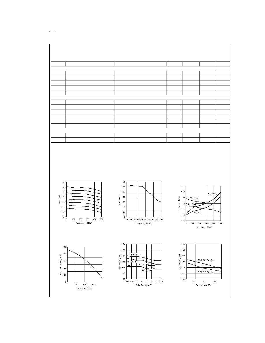
Typical Performance Characteristics
(V
CC
= +5V, R
L
= 1 k
, max gain; unless specified)
Gain vs Frequency
DS015016-3
Transconductance vs Frequency
DS015016-4
2nd and 3rd Harmonic Distortion
vs Frequency
DS015016-5
2-Tone, 3rd Order Intermodulation
Output Intercept vs Frequency
DS015016-6
Distortion vs Gain Setting
DS015016-7
Distortion vs Temperature
DS015016-8
www.national.com
4
Typical Performance Characteristics
(V
CC
= +5V, R
L
= 1 k
, max gain; unless
specified) (Continued)
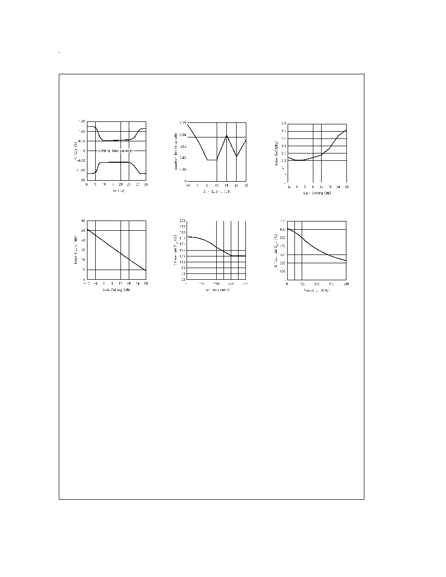
6 dB Gain Step, Time Domain
Response
DS015016-9
Gain Step Error Deviation
vs Gain Setting
DS015016-10
Input Referred Thermal Noise vs
Gain Setting (Gain Block)
DS015016-11
Noise Figure vs Gain Setting
DS015016-12
Differential Z
IN
vs Frequency
DS015016-13
Differential Z
OUT
vs Frequency
DS015016-14
www.national.com
5