©2004 National Semiconductor Corporation DS200286
www.national.com
Revision 1.6
CL
C5903 Du
al Dig
i
tal T
u
n
e
r / A
G
C
June 2004
N a t i o n a l S e m i c o n d u c t o r
CLC5903
Dual Digital Tuner / AGC
0
0
General Overview
The CLC5903 Dual Digital Tuner / AGC IC is a two channel
digital downconverter (DDC) with integrated automatic gain
control (AGC). The CLC5903 is a key component in the
Enhanced Diversity Receiver Chipset (EDRCS) which
includes one CLC5903 Dual Digital Tuner / AGC, two
CLC5957 12-bit analog-to-digital converters (ADCs), and two
CLC5526 digitally controlled var iable gain amplifiers
(DVGAs). This system allows direct IF sampling of signals up
to 300MHz for enhanced receiver performance and reduced
system costs.
The CLC5903 is an enhanced replacement for the CLC5902
in the Diversity Receiver Chipset (DRCS). The m ain
improvements relative to the CLC5902 are a 50% increase in
maximum sample rate from 52MHz to 78MHz, a 62%
reduction in power consumption from 760mW to 290mW,
and the added flexibility to independently program filter
coefficients in the two channels. A block diagram for a
DRCS-based narrowband communications system is shown
in Figure 1.
The CLC5903 offers high dynamic range digital tuning and
filtering based on hard-wired digital signal processing (DSP)
technology. Each channel has independent tuning, phase
offset, filter coefficients, and gain settings. Channel filtering
is performed by a series of three filters. The first is a 4-stage
Cascaded Integrator Comb (CIC) filter with a programmable
decim at ion ratio fr om 8 to 20 48. Next t her e a re two
symmetric FIR filters, a 21-tap and a 63-tap, both with
independent programmable coefficients. The first FIR filter
decimates the data by 2, the second FIR decimates by either
2 or 4. Channel filter bandwidth at 52MSPS ranges from
±650kHz down to ±1.3kHz. At 78MSPS, the maximum
bandwidth increases to ±975kHz.
The CLC5903's AGC controller monitors the ADC output and
controls the ADC input signal level by adjusting the DVGA
setting. AGC threshold, deadband+hysteresis, and the loop
time constant are user defined. Total dynamic range of
greater than 120dB full-scale signal to noise in a 200kHz
bandwidth can be achieved with the Diversity Receiver
Chipset.
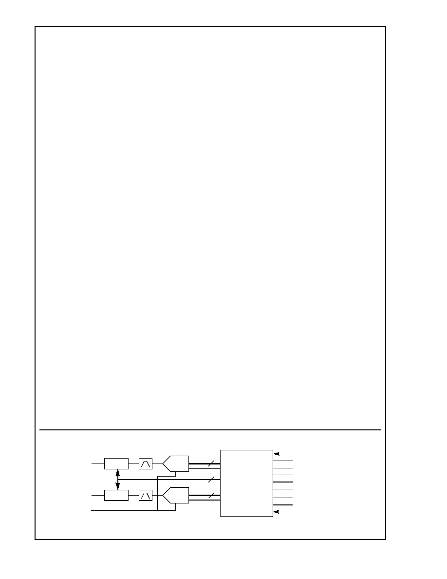
Figure 1. Diversity Receiver Chipset Block Diagram
DVGA
IF A
SerialOutA/B
SerialOutB
SCK
SFS
RDY
LC
DVGA
IF B
LC
ParallelOutput[15..0]
ParallelOutputEnable
ParallelSelect[2..0]
CLC5526
CLC5957
CLC5903
CLK
12
8
12
ADC
ADC
SCK_IN
Dual Digital
Tuner/AGC
DAV
DAV
Features
78MSPS Operation
Low Power, 145mW/channel, 52 MHz, Dec=192
Two Independent Channels with 14-bit inputs
Serial Daisy-chain Mode for quad receivers
Greater than 100 dB image rejection
Greater than 100 dB spurious free dynamic range
0.02 Hz tuning resolution
User Programmable AGC with enhanced Power Detector
Channel Filters include a Fourth Order CIC followed by
21-tap and 63-tap Symmetric FIRs
FIR filters process 21-bit Data with 16-bit Programmable
Coefficients
Two independent FIR coefficient memories which can be
routed to either or both channels.
Flexible output formats include 12-bit Floating Point or 8,
16, 24, and 32 bit Fixed Point
Serial and Parallel output ports
JTAG Boundary Scan
8-bit Microprocessor Interface
128 pin PQFP and 128 pin FBGA packages
100% Software compatible with the CLC5902
Pin compatible with the CLC5902 except for V
DD
voltage
Applications
Cellular Basestations
Satellite Receivers
Wireless Local Loop Receivers
Digital Communications
N
www.national.com
2
CLC
5
9
0
3
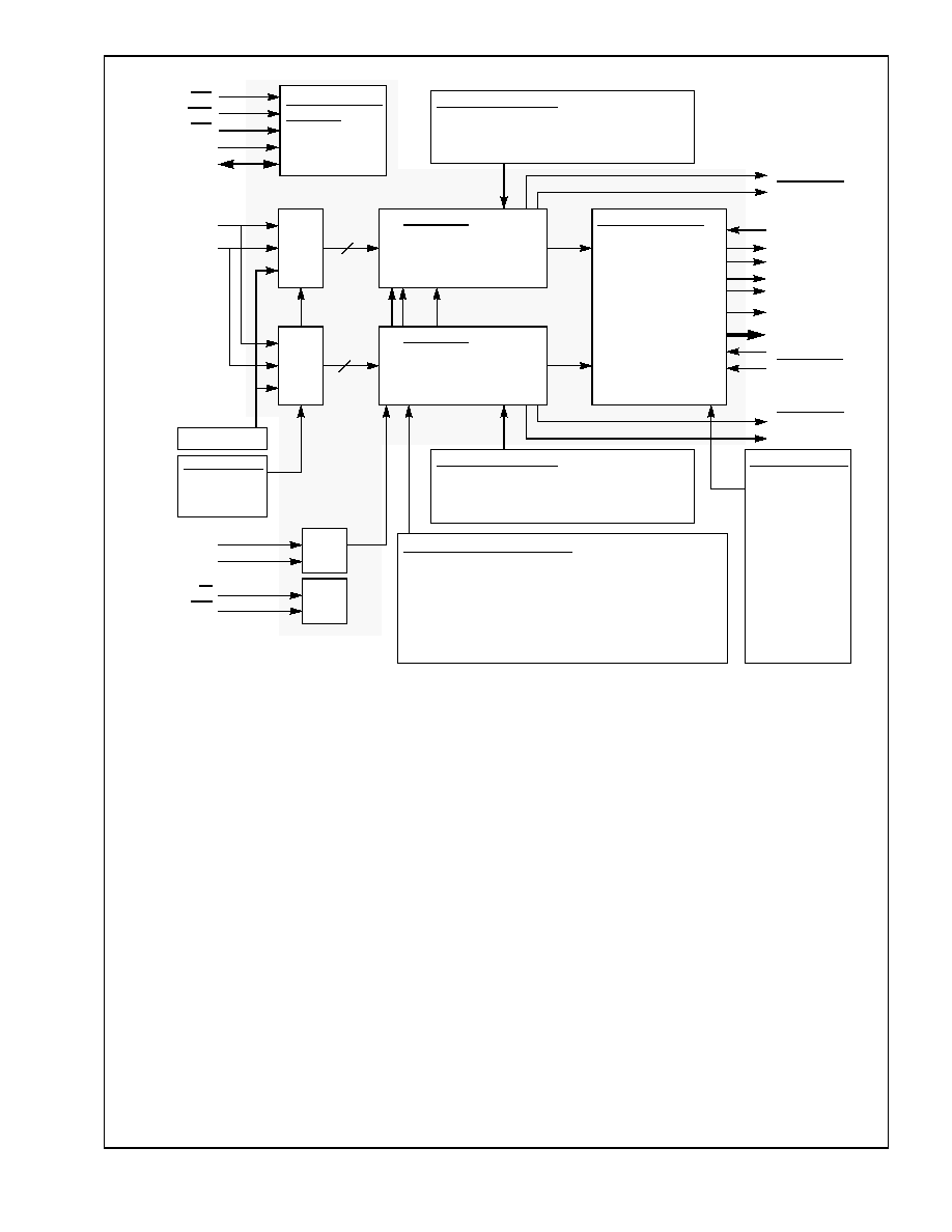
Functional Description
The CLC5903 block diagram is shown in Figure 2. The
CLC5903 contains two identical digital down-conversion
(DDC) circuits. Each DDC accepts an independently clocked
14-bit sample at up to 78MSPS, down conver ts from a
selected carrier frequency to baseband, decimates the signal
rate by a programmable factor ranging from 32 to 16384, pro-
vides channel filtering, and outputs quadrature symbols.
A crossbar switch enables either of the two inputs or a test
register to be routed to either DDC channel. Flexible channel
filtering is provided by the two programmable decimating FIR
filters. The final filter outputs can be converted to a 12-bit
floating point format or standard two's complement format.
The output data is available at both serial and parallel ports.
The CLC5903 maintains over 100 dB of spurious free
dynamic range and over 100 dB of out-of-band rejection.
This allows considerable latitude in channel filter partitioning
between the analog and digital domains.
The frequencies, phase offsets, and phase dither of the two
sine/cosine numerically controlled oscillators (NCOs) can be
independently specified. Two sets of coefficient memories
and a crossbar switch allow shared or independent filter
coefficients and bandwidth for each channel. Both channels
share the same decimation ratio and input/output formats.
Each channel has its own AGC circuit for use with narrow-
band radio channels where most of the channel filtering pre-
cedes the ADC. The AGC closes the loop around the
CLC5526 DVGA, compressing the dynamic range of the sig-
nal into the ADC. AGC gain compensation in the CLC5903
removes the DVGA gain steps at the output. The time align-
ment of this gain compensation circuit can be adjusted to
support ADCs with different latencies. The AGC can be con-
figured to operate continuously or set to a fixed gain step.
The two AGC circuits operate independently but share the
same programmed parameters and control signals.
The chip receives configuration and control information over
a microprocessor-compatible bus consisting of an 8-bit data
I/O port, an 8-bit address port, a chip enable strobe, a read
strobe, and a write strobe. The chip's control registers (8 bits
each) are memory mapped into the 8-bit address space of
the control port. Page select bits allow access to the overlaid
A and B set of FIR coefficients.
JTAG boundary scan and on-chip diagnostic circuits are pro-
vided to simplify system debug and test.
The CLC5903 supports 3.3V I/O even though the core logic
voltage is 1.8V. The CLC5903 outputs swing to the 3.3V rail
so they can be directly connected to 5V TTL inputs if desired.
Figure 2. CLC5903 Dual Digital Tuner / AGC Block Diagram with Control Register Associations
AIN
BIN
MUX
MUX
Input Source
Output Controls
Output Formatter
Floating Point:
32-bit Truncated or
24-bit Rounded or
16-bit Rounded or
8-bit Truncated
Two's Complement:
4-bit Exponent and
8-bit Mantissa
or
AOUT/BOUT
BOUT
SCK
SFS
RDY
POUT[15..0]
PSEL[2..0]
POUT_EN
A_SOURCE
B_SOURCE
RATE
SOUT_EN
SCK_POL
SFS_POL
RDY_POL
MUX_MODE
PACKED
FORMAT
DEBUG_EN
DEBUG_TAP
CKA
CLK
GEN
TEST_REG
Channel B Controls
GAIN_B
FREQ_B
PHASE_B
AGC_IC_B AGC_RB_B
DITH_B
Common Channel Controls
DEC_BY_4
SCALE
EXP_INH
AGC_HOLD_IC
AGC_LOOP_GAIN
AGC_TABLE
F1B_COEFF
F2B_COEFF
AGAIN[2..0]
ASTROBE
BGAIN[2..0]
BSTROBE
Microprocessor
Interface
RD
WR
CE
A[7:0]
D[7:0]
SI
MR
Sync
Logic
14
14
DEC
A
B
Channel A
Tuning,
Channel Filters, and
AGC (see Figure 16)
Channel B
Tuning,
Channel Filters, and
AGC (see Figure 16)
(see Figure 29)
SCK_IN
SFS_MODE
SDC_EN
AGC_COMB_ORD
EXT_DELAY
COEF_SEL_F1B
COEF_SEL_F2B
Channel A Controls
GAIN_A
FREQ_A
PHASE_A
AGC_IC_A AGC_RB_A
DITH_A
COEF_SEL_F1A
COEF_SEL_F2A
F1A_COEFF
F2A_COEFF
PAGE_SEL_F1
PAGE_SEL_F2
CKB
3
www.national.com
C
L
C
5
903
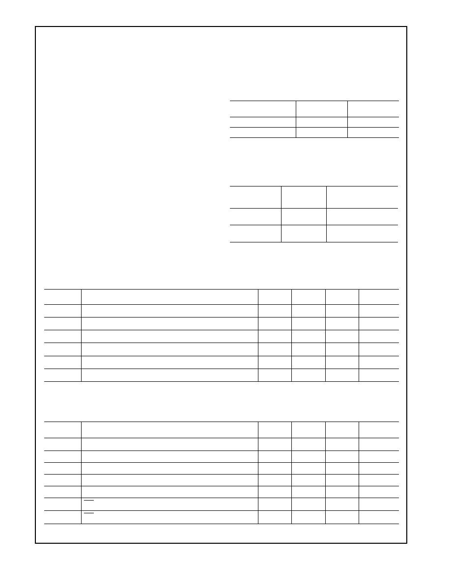
Absolute Maximum Ratings
NOTE: Absolute maximum ratings are limiting values, to be
applied individually, and beyond which the serviceability of the
circuit may be impaired. Functional operability under any of
these conditions is not necessarily implied. Exposure to maxi-
mum ratings for extended periods may affect device reliability.
Operating Ratings
Package Thermal Resistance
Reliability Information
Ordering Information
CLC5903 Electrical Characteristics
(Note 1)
Positive IO Supply Voltage (V
DDIO
)
-0.3V to 4.2V
Positive CoreSupply Voltage (V
DD
)
-0.3V to 2.4V
Voltage on Any Input or Output Pin
-0.3V to V
DDIO
+0.5V
Input Current at Any Pin
±25mA
Package Input Current
±50mA
Package Dissipation at T
A
=25∞C
1W
ESD Susceptibility
Human Body Model
Machine Model
2000V
200V
Soldering Temperature, Infrared, 10
seconds
300∞C
Storage Temperature
-65∞C to 150∞C
Positive IO Supply Voltage (V
DDIO
)
3.3V ±10%
Positive Core Supply Voltage (V
DD
)
1.8V ±10%
Operating Temperature Range
-40∞C to +85∞C
Package
ja
jc
128 pin PQFP
39∞C/W
20∞C/W
128 pin FBGA
30∞C/W
N/A
Transistor Count
1.4 million
Order Code
Temperature
Range
Description
CLC5903VLA
-40∞C to
+85∞C
128-pin PQFP (indus-
trial temperature range)
CLC5903SM
-40∞C to
+85∞C
128-pin FBGA (indus-
trial temperature range)
DC Characteristics
(F
S
=78MHz, CIC Decimation=48, F2 Decimation=2; unless specified)
Symbol
Parameter
Min
Typ
Max
Units
V
IL
Voltage input low
-0.5
0.7
V
V
IH
Voltage input high
2.3
V
DDIO
+0.5
V
I
OZ
Input current
20
uA
V
OL
Voltage output low (I
OL
= 4mA/16mA, see Note 2)
0.4
V
V
OH
Voltage output high (I
OH
= -4mA/-16mA, see Note 2)
2.4
V
C
IN
Input capacitance
5.0
pF
AC Characteristics
(F
S
=78MHz, CIC Decimation=48, F2 Decimation=2; unless specified)
Symbol
Parameter (C
L
=50pF)
Min
Typ
Max
Units
F
CK
Clock (CKA|B) Frequency (Figure 7)
78
MHz
SFDR
Spurious Free Dynamic Range
-100
dBFS
SNR
Signal to Noise Ratio
-127
dBFS
Tuning Resolution
0.02
Hz
Phase Resolution
0.005
∞
t
MRA
MR Active Time (Figure 5)
4
CK periods
t
MRIC
MR Inactive to first Control Port Access (Figure 5)
10
CK periods
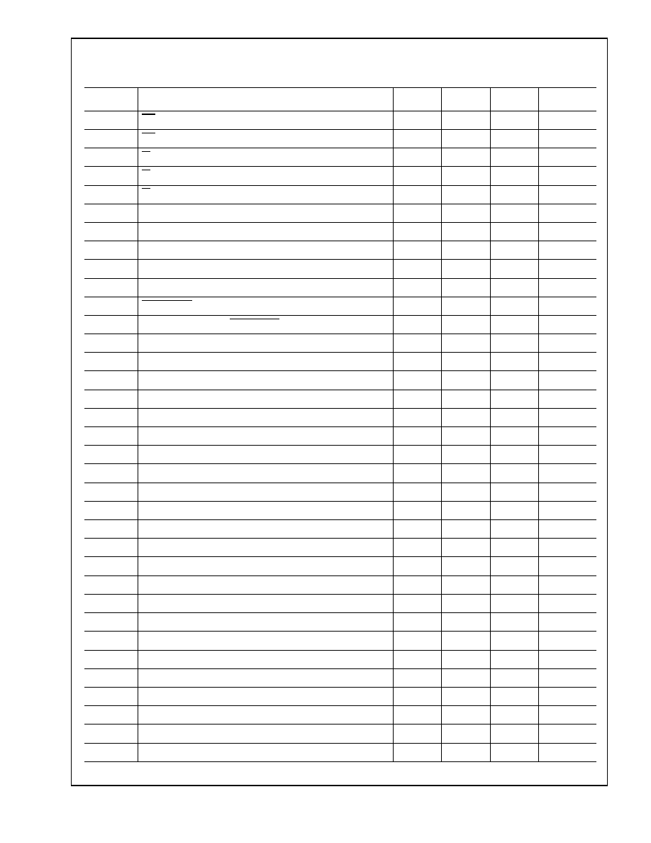
www.national.com
4
CLC
5
9
0
3
t
MRSU
MR Setup Time to CKA|B (Figure 5)
6
ns
t
MRH
MR Hold Time to CKA|B (Figure 5)
2
ns
t
SISU
SI Setup Time to CKA|B (Figure 6)
6
ns
t
SIH
SI Hold Time from CKA|B (Figure 6)
2
ns
t
SIW
SI Pulse Width (Figure 6)
4
CK periods
t
CKDC
CKA|B duty cycle (Figure 7)
40
60
%
t
RF
CKA|B rise and fall times (V
IL
to V
IH
) (Figure 7)
2
ns
t
SU
Input setup before CKA|B goes high (A|BIN) (Figure 7)
3
ns
t
HD
Input hold time after CKA|B goes high (A|BIN) (Figure 7)
1
ns
t
CKL
Minimum time low for CK = CKA | CKB (Figure 8)
3.1
ns
t
STIW
A|BSTROBE Inactive Pulse Width (Figure 9)
2
CK period
t
GSTB
A|BGAIN setup before A|BSTROBE (Figure 9)
6
ns
t
SFSV
SCK to SFS Valid (Note 3) (Figure 10)
-1
5
ns
t
OV
SCK to A|BOUT Valid (Note 4) (Figure 10)
-1
5
ns
t
RDYW
RDY Pulse Width (Figure 10)
2
CK periods
t
RDYV
SCK to RDY valid (Figure 10)
-1
5
ns
t
OENV
POUT_EN Active to POUT[15..0] Valid (Figure 11)
12
ns
t
OENT
POUT_EN Inactive to POUT[15..0] Tri-State (Figure 11)
10
ns
t
SELV
PSEL[2..0] to POUT[15..0] Valid (Figure 12)
13
ns
t
POV
RDY to POUT[15..0] New Value Valid (Note 5) (Figure 13)
7
ns
t
JPCO
Propagation Delay TCK to TDO (Figure 14)
25
ns
t
JSCO
Propagation Delay TCK to Data Out (Figure 14)
35
ns
t
JPDZ
Disable Time TCK to TDO (Figure 14)
25
ns
t
JSDZ
Disable Time TCK to Data Out (Figure 14)
35
ns
t
JPEN
Enable Time TCK to TDO (Figure 14)
0
25
ns
t
JSEN
Enable Time TCK to Data Out (Figure 14)
0
35
ns
t
JSSU
Setup Time Data to TCK (Figure 14)
10
ns
t
JPSU
Setup Time TDI, TMS to TCK (Figure 14)
10
ns
t
JSH
Hold Time Data to TCK (Figure 14)
45
ns
t
JPH
Hold Time TCK to TDI, TMS (Figure 14)
45
ns
t
JCH
TCK Pulse Width High (Figure 14)
50
ns
t
JCL
TCK Pulse Width Low (Figure 14)
40
ns
JTAG
FMAX
TCK Maximum Frequency (Figure 14)
10
MHz
t
CSU
Control Setup before the controlling signal goes low (Figure 15)
5
ns
t
CHD
Control hold after the controlling signal goes high (Figure 15)
5
ns
AC Characteristics
(Continued)
(F
S
=78MHz, CIC Decimation=48, F2 Decimation=2; unless specified)
Symbol
Parameter (C
L
=50pF)
Min
Typ
Max
Units
5
www.national.com
C
L
C
5
903
Note 1:
Datasheet min/max specification limits are guaranteed by design, test, or statistical analysis.
Note 2:
All output pins provide 16mA output drive except TDO (pin 116) which provides 4mA output drive.
Note 3:
t
SFSV
refers to the rising edge of SCK when SCK_POL=0 and the falling edge when SCK_POL=1.
Note 4:
t
OV
refers to the rising edge of SCK when SCK_POL=0 and the falling edge when SCK_POL=1.
Note 5:
t
RDYV
refers to the rising edge of RDY when RDY_POL=0 and the falling edge when RDY_POL=1.
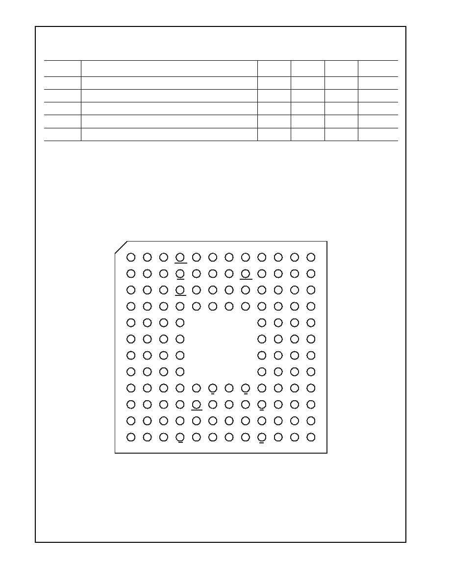
CLC5903SM Pinout
t
CSPW
Controlling strobe pulse width (Write) (Figure 15)
30
ns
t
CDLY
Control output delay controlling signal low to D (Read) (Figure 15)
30
ns
t
CZ
Control tri-state delay after controlling signal high (Figure 15)
20
ns
I
DD
Dynamic Supply Current (F
CK
=78MHz, N=48, SCK=39MHz)
120
200
mA
I
DDIO
Dynamic Supply Current (F
CK
=78MHz, N=48, SCK=39MHz)
65
100
mA
AC Characteristics
(Continued)
(F
S
=78MHz, CIC Decimation=48, F2 Decimation=2; unless specified)
Symbol
Parameter (C
L
=50pF)
Min
Typ
Max
Units
Figure 3. CLC5903SM FBGA Pinout
A12
A1
A2
A3
A4
A5
A6
A7
A8
A9
A10
A11
B12
B1
B2
B3
B4
B5
B6
B7
B8
B9
B10
B11
C12
C1
C2
C3
C4
C5
C6
C7
C8
C9
C10
C11
D12
D1
D2
D3
D4
D5
D6
D7
D8
D9
D10
D11
E12
E1
E2
E3
E4
E9
E10
E11
F12
F1
F2
F3
F4
F9
F10
F11
G12
G1
G2
G3
G4
G9
G10
G11
H12
H1
H2
H3
H4
H9
H10
H11
J12
J1
J2
J3
J4
J5
J6
J7
J8
J9
J10
J11
K12
K1
K2
K3
K4
K5
K6
K7
K8
K9
K10
K11
L12
L1
L2
L3
L4
L5
L6
L7
L8
L9
L10
L11
M12
M1
M2
M3
M4
M5
M6
M7
M8
M9
M10
M11
AIN12
AIN10
AIN7
AIN5
AIN2
VSS
VDD
BIN10
BIN7
BIN4
BIN1
NC
VDDIO
VSSIO
AIN11
AIN8
AIN1
CKA
BIN13
BIN11
BIN8
BIN2
VSS
VDDIO
AGAIN1
NC
NC
AIN13
AIN6
AIN3
BIN12
BIN9
BIN6
BIN0
NC
BGAIN0
SCAN_EN
TRST
ASTROB
AGAIN2
AIN9
AIN4
AIN0
BIN5
BIN3
CKB
BGAIN1
MR
TCK
TMS
VSS
AGAIN0
BGAIN2
BSTROB
NC
A[7]
VDD
TDO
TDI
POUT_SEL2
SI
VSSIO
A[6]
VDD
POUT_SEL1
POUT_SEL0
POUT0
POUT1
NC
A[4]
A[5]
VSS
VSSIO
POUT_EN
POUT2
VSS
CE
A[1]
A[3]
A[2]
VDDIO
POUT4
NC
POUT7
POUT9
SFS
RDY
D[2]
D[7]
RD
A[0]
WR
POUT3
NC
VSSIO
VDDIO
VSSIO
POUT14
BOUT
D[0]
VSSIO
NC
D[6]
VSSIO
NC
SCK_IN
POUT6
POUT11
POUT13
VDD
VSSIO
SCK
D[1]
D[4]
NC
VDDIO
NC
POUT5
POUT8
POUT10
POUT12
POUT15
AOUT
VDDIO
VSS
VDD
D[3]
D[5]
Top View