© 1999 National Semiconductor Corporation
http://www.national.com
Printed in the U.S.A.
N
General Description
The CLC5957 is a monolithic 12-bit, 70MSPS analog-to-digital
converter. The device has been optimized for use in IF-sampled
digital receivers and other applications where high resolution,
high sampling rate, wide dynamic range, low power dissipation,
and compact size are required. The CLC5957 features differential
analog inputs, low jitter differential universal clock inputs, a low
distortion track-and-hold with 0-300MHz input bandwidth, a band-
gap voltage reference, data valid clock output, TTL compatible
CMOS (3.3V or 2.5V) programmable output logic, and a propri-
etary 12-bit multi-stage quantizer. The CLC5957 is fabricated on
the ABIC-V 0.8 micron BiCMOS process.
The CLC5957 features a 74dBc spurious free dynamic range
(SFDR) and a 67dB signal to noise ratio (SNR). The wideband
track-and-hold allows sampling of IF signals to greater than
250MHz. The part produces two-tone, dithered, SFDR of 83dBFS
at 75MHz input frequency. The differential analog input provides
excellent common mode rejection, while the differential universal
clock inputs minimize jitter. The 48-pin TSSOP package provides
an extremely small footprint for applications where space is a
critical consideration. The CLC5957 operates from a single +5V
power supply. Operation over the industrial temperature range of
-40∞C to +85∞C is guaranteed. National Semiconductor tests
each part to verify compliance with the guaranteed specifications.
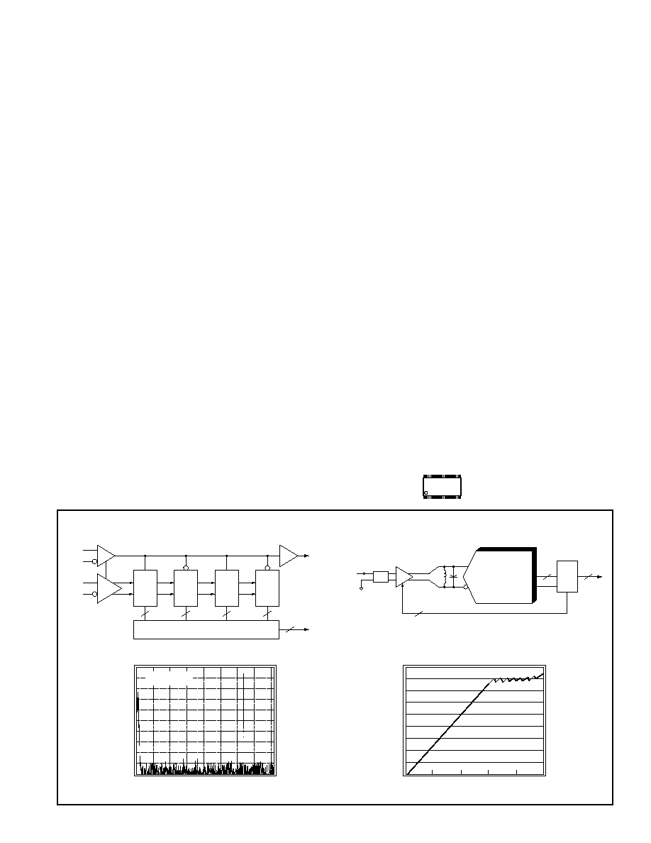
ADC Block Diagram
CLC5957
12-bit, 70MSPS Broadband Monolithic A/D Converter
Features
∑ 70MSPS
∑ Wide dynamic range
SFDR: 74dBc
SFDR w/dither: 85dBFS
SNR: 67dB
∑ IF sampling capability
∑ Input bandwidth = 0-300MHz
∑ Low power dissipation: 640mW
∑ Very small package: 48-pin TSSOP
∑ Single +5V supply
∑ Data valid clock output
∑ Programmable output levels:
3.3V or 2.5V
Applications
∑ Cellular base-stations
∑ Digital communications
∑ Infrared/CCD imaging
∑ IF sampling
∑ Electro-optics
∑ Instrumentation
∑ Medical imaging
∑ High definition video
October 1999
CLC5957
12-bit,
70MSPS Br
oadband Monolithic A/D Con
ver
ter
3-bit
Q
T/H
A
In
3
3-bit
Q
3
3-bit
Q
3
3-bit
Q
3
Bit Align/Error Correct
12
Clock
In
ADC
Out
DAV
12
IF
Saw
IF
Input
~
~
BPF
(150MHz
typ.)
DVGA
(
G = 42dB)
CLC5957
12-bit
70MSPS
ADC
Dig.
Tuner/
Filter
AGC
20
3-bit (Gain Control)
Noise
BPF
DAV
CLC5902
First IF Receiver
ME79TG
CL5956
IMTD
N
ME79TG
CL5956
IMTD
N
ME79TG
CL5956
IMTD
N
ME79TG
CLC5957
MTD
N
Actual Size
Output Level (dBFS)
Frequency (MHz)
0
-10
-100
-90
-80
-70
-60
-50
-40
-30
-20
0
8
28
4
12
16
20
24
32
F
in
= 25.3MHZ
F
sample
= 66MHz
Single Tone Output Spectrum w/Dither
SINAD dBc (BW = 216KHz)
Input (dBFS)
90
80
0
10
20
30
40
50
60
70
-125
-50
-25
0
-75
-100
Receiver SINAD vs. Input Amplitude
Decimation/filter = 190/0.8
Output BW = 50M/190 X 0.8 = 210KHz

http://www.national.com
2
CLC5957 Electrical Characteristics
(V
cc
= +5V, 66MSPS; unless specified) (T
min
= -40∞C, T
max
= +85∞C)
PARAMETERS
CONDITIONS TEMP
RATINGS
UNITS
NOTES
MIN TYP
MAX
2
RESOLUTION
Full
12
Bits
1
DIFF. INPUT VOLTAGE RANGE
Full
2.048
V
MAXIMUM CONVERSION RATE
Full
70
75
MSPS
1
SNR
f
in
= 25MHz, A
in
= -1dBFS
+25∞C
63
66
dBFS
1
SFDR
f
in
= 25MHz, A
in
= -1dBFS
+25∞C
66
74
dBc
1
NO MISSING CODES
f
in
= 5MHz, A
in
= -1dBFS
+25∞C
Guaranteed
1
DYNAMIC PERFORMANCE
large-signal bandwidth
A
in
= -3dBFS
+25∞C
300
MHz
overvoltage recovery time
A
in
= 1.5FS (0.01%)
+25∞C
12
ns
effective aperture delay (Ta)
+25∞C
-0.41
ns
aperture jitter
+25∞C
0.3
ps(rms)
NOISE AND DISTORTION
signal-to-noise ratio (w/o 50 harmonics)
f
in
= 5.0MHz
A
in
= -1dBFS
Full
67
dBFS
f
in
= 25MHz
A
in
= -1dBFS
Full
60
66
dBFS
1
f
in
= 75MHz
A
in
= -3dBFS
Full
65
dBFS
f
in
= 150MHz
A
in
= -15dBFS
Full
66
dBFS
f
in
= 250MHz
A
in
= -15dBFS
Full
66
dBFS
spurious-free dynamic range
f
in
= 5.0MHz
A
in
= -1dBFS
Full
74
dBc
f
in
= 25MHz
A
in
= -1dBFS
Full
60
74
dBc
1
f
in
= 75MHz
A
in
= -3dBFS
Full
72
dBc
f
in
= 150MHz
A
in
= -15dBFS
Full
69
dBc
f
in
= 250MHz
A
in
= -15dBFS
Full
65
dBc
intermodulation distortion
f
in1
= 149.84MHz, f
in2
= 149.7MHz A
in
= -10dBFS
+25∞C
68
dBFS
f
in1
= 249.86MHz, f
in2
= 249.69MHz A
in
= -10dBFS
+25∞C
58
dBFS
dithered performance
spurious-free dynamic range
f
in
= 19MHz
A
in
= -6dBFS
+25∞C
85
dBFS
intermodulation distortion
f
in1
= 74MHz, f
in2
= 75MHz
A
in
= -12dBFS
+25∞C
83
dBFS
DC ACCURACY AND PERFORMANCE
differential non-linearity
f
in
= 5MHz, A
in
= -1dBFS
Full
±0.65
LSB
integral non-linearity
f
in
= 5MHz, A
in
= -1dBFS
Full
±1.5
LSB
no missing codes
f
in
= 5MHz, A
in
= -1dBFS
Full
Guaranteed
1
offset error
Full
-30
0
30
mV
1
gain error
Full
1.2
%FS
V
ref
Full
2.2
2.37
2.6
V
1
ANALOG INPUTS
analog differential input voltage range
Full
2.048
V
pp
analog input resistance (single ended)
Full
500
analog input resistance (differential)
Full
1000
analog input capacitance (single-ended)
Full
2
pF
ENCODE INPUTS (Universal)
VIH
+25∞C
5
V
3
VIL
+25∞C
0
V
3
differential input swing
+25∞C
0.2
V
3
DIGITAL OUTPUTS
output voltage
logic LOW
+25∞C
0.01
0.4
V
1
OUTLEV = 1 (open)
logic HIGH
+25∞C
3.2
3.5
3.8
V
1
OUTLEV = 0 (GND)
logic HIGH
+25∞C
2.4
2.7
3.0
V
1
TIMING (C load < 7pF)
maximum conversion rate
Full
70
75
MSPS
1
minimum conversion rate
+25∞C
10
MSPS
pulse width high
Full
7.2
ns
pulse width low
Full
7.2
ns
pipeline latency
Full
3.0
clk cycle
falling ENCODE to output change (50%) (Tod)
+25∞C
10
ns
rising ENCODE to DAV change (50%) (Tdv)
+25∞C
9.6
ns
3
http://www.national.com
PARAMETERS
CONDITIONS TEMP
RATINGS
UNITS
NOTES
MIN TYP
MAX
2
POWER REQUIREMENTS
+5V supply current
Full
128
150
mA
1
Power dissipation
Full
640
750
mW
1
V
CC
power supply rejection ratio
+25∞C
64
dB
Min/max ratings are based on product characterization and simulation. Individual parameters are tested as noted. Outgoing quality levels are
determined from tested parameters.
Absolute Maximum Ratings
positive supply voltage (V
cc
)
-0.5V to +6V
differential voltage between any two grounds
<100mV
analog input voltage range
GND to V
cc
digital input voltage range
-0.5V to +V
cc
output short circuit duration (one-pin to ground)
infinite
junction temperature
175∞C
storage temperature range
-65∞C to 150∞C
lead solder duration (+300∞C)
10sec
Note: Absolute maximum ratings are limiting values, to be applied individually, and
beyond which the serviceability of the circuit may be impaired. Functional
operability under any of these conditions is not necessarily implied. Exposure to
maximum ratings for extended periods may affect device reliability.
Recommended Operating Conditions
positive supply voltage (V
cc
)
+5V ±5%
analog input voltage range
2.048V
pp
diff.
operating temperature range
-40∞C to +85∞C
Package Thermal Resistance
Package
JA
JC
48-pin TSSOP
56∞C/W
16∞C/W
Reliability Information
Transistor count
5000
Ordering Information
Model
Temperature Range
Description
CLC5957MTD
-40∞C to +85∞C
48-pin TSSOP
CLC5957PCASM
Fully loaded evaluation board with CLC5957 ... ready for test.
ANALOG
INPUT
ENCODE
CLOCK
DAV
CLOCK
DATA
OUTPUT
N
Ta = -410ps
Tdv = 9.6ns
Tod = 10ns
N+1
N+2
N
N+1
N+2
N-3
N-2
N-1
CLC5957 Timing Diagram
Notes
1) These parameters are 100% tested at 25∞C. Sample tested at full
temperature range.
2) Typical specifications are based on the mean test values of
deliverable converters from the first three diffusion lots.
3) See page 7, Figure 3 for ENCODE Inputs circuit.
CLC5957 Electrical Characteristics
(V
cc
= +5V, 66MSPS; unless specified) (T
min
= -40∞C, T
max
= +85∞C)
http://www.national.com
4
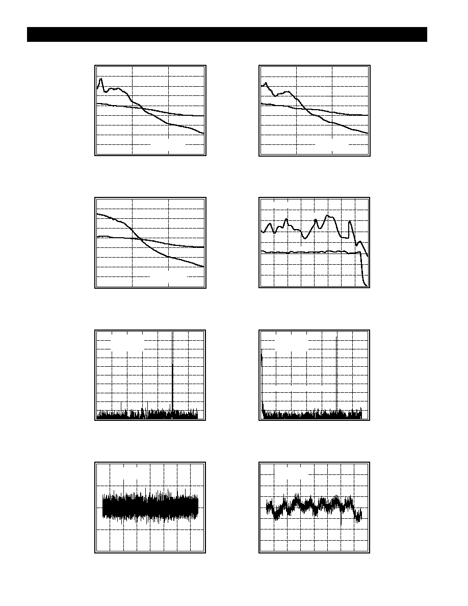
CLC5957 Typical Performance Characteristics
(V
cc
= +5V)
SNR and SFDR vs. Input Frequency
SNR (dBFS) and SFDR (dBc)
Input Frequency (MHz)
85
40
45
50
55
60
65
70
75
80
0
200
300
SFDR
100
SNR
F
s
= 40.96MSPS
A
in
= -3dBFS
SNR and SFDR vs. Input Frequency
SNR (dBFS) and SFDR (dBc)
Input Frequency (MHz)
85
40
45
50
55
60
65
70
75
80
0
200
300
SFDR
100
SNR
F
s
= 52MSPS
A
in
= -3dBFS
SNR and SFDR vs. Input Frequency
SNR (dBFS) and SFDR (dBc)
Input Frequency (MHz)
85
40
45
50
55
60
65
70
75
80
0
200
300
SNR
100
SFDR
F
s
= 66MSPS
A
in
= -3dBFS
SFDR
SNR and SFDR vs. Sample Rate
SNR (dBc) and SFDR (dBc)
Sample Rate (MSPS)
50
55
60
65
70
80
90
40
50
60
70
80
SNR
F
in
= 24.5MHz
75
85
Single Tone Output Spectrum
Output Level (dBFS)
Frequency (MHz)
-100
-90
-70
-60
-40
-20
0
0
5
10
15
35
-30
-10
20
25
30
-50
-80
F
s
= 66MSPS
A
in
= -1dBFS
F
in
= 24.5MHz
Differential Non-Linearity
DNL (LSBs)
Output Code
-1.0
1.0
0
512 1024 1536
3584
0.5
2048 2560 3072
0
-0.5
4096
F
s
= 66MSPS
F
in
= 5MHz
Integral Non-Linearity
INL (LSBs)
Output Code
-2.0
2.0
0
512 1024 1536
3584
1.0
2048 2560 3072
0
-1.0
-0.5
1.5
0.5
-1.5
4096
F
s
= 66MSPS
F
in
= 5MHz
Single Tone Output Spectrum (w/Dither)
Output Level (dBFS)
Frequency (MHz)
-100
-90
-70
-60
-40
-20
0
0
5
10
15
35
-30
-10
20
25
30
-50
-80
F
s
= 66MSPS
A
in
= - 6dBFS
F
in
= 24.5MHz
Dither Signal = 500kHz @ - 28dBFS
5
http://www.national.com
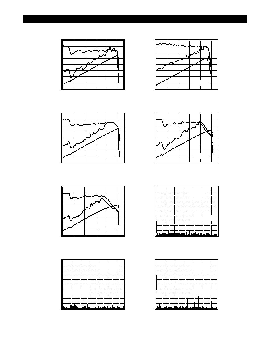
CLC5957 Typical Performance Characteristics
(V
cc
= +5V)
SNR
SNR and SFDR vs.
Input Amplitude (w/Dither)
SNR (dBc), SFDR (dBc), & THD (dBFS)
Input Amplitude (dBFS)
10
20
30
40
50
60
90
-50
-40
-30
-20
-10
0
SFDR
F
in
= 20MHz
F
s
= 66MSPS
SNR
SNR (dBc), SFDR (dBc), & THD (dBFS)
Input Amplitude (dBFS)
SFDR
F
in
= 75MHz
F
s
= 66MSPS
SNR
SFDR
F
in
= 150MHz
F
s
= 66MSPS
SNR and SFDR vs.
Input Amplitude (w/o Dither)
SNR and SFDR vs.
Input Amplitude (w/o Dither)
SNR (dBc), SFDR (dBc), & THD (dBFS)
Input Amplitude (dBFS)
10
90
-50
-40
-30
70
-20
-10
50
30
80
60
40
20
0
SNR
SFDR
THD
F
in
= 20MHz
F
s
= 66MSPS
70
80
THD
THD
10
90
-50
-40
-30
70
-20
-10
50
30
80
60
40
20
0
SNR
SNR (dBc), SFDR (dBc), & THD (dBFS)
Input Amplitude (dBFS)
SFDR
F
in
= 250MHz
F
s
= 66MSPS
SNR and SFDR vs.
Input Amplitude (w/o Dither)
THD
10
90
-50
-40
-30
70
-20
-10
50
30
80
60
40
20
0
SNR (dBc), SFDR (dBc), & THD (dBFS)
Input Amplitude (dBFS)
SNR and SFDR vs.
Input Amplitude (w/o Dither)
10
90
-50
-40
-30
70
-20
-10
50
30
80
60
40
20
0
THD
Two Tone Output Spectrum (w/Dither)
Output Level (dBFS)
Frequency (MHz)
-100
-90
-80
-70
-60
-50
-40
-30
-20
-10
0
0
20
F
s
= 66MSPS
F1 = 249.5MHz
F2 = 251.5MHz
5
10
15
25
30
Two Tone Output Spectrum (w/Dither)
Output Level (dBFS)
Frequency (MHz)
-100
-90
-80
-70
-60
-50
-40
-30
-20
-10
0
F
s
= 66MSPS
F1 = 149.5MHz
F2 = 150.5MHz
0
20
5
10
15
25
30
Two Tone Output Spectrum (w/Dither)
Output Level (dBFS)
Frequency (MHz)
-100
-90
-80
-70
-60
-50
-40
-30
-20
-10
0
0
20
5
10
15
25
30
F
s
= 66MSPS
F1 = 74.5MHz
F2 = 75.5MHz
Dither Signal =
300KHz @ -28dBFS
Dither Signal =
500KHz @ -28dBFS
Dither Signal =
300KHz @ -28dBFS