CLC5957
12-Bit, 70 MSPS Broadband Monolithic A/D Converter
General Description
The CLC5957 is a monolithic 12-bit, 70MSPS analog-to-
digital converter. The device has been optimized for use in
IF-sampled digital receivers and other applications where
high resolution, high sampling rate, wide dynamic range, low
power dissipation, and compact size are required. The
CLC5957 features differential analog inputs, low jitter differ-
ential universal clock inputs, a low distortion track-and-hold
with 0-300MHz input bandwidth, a bandgap voltage refer-
ence, data valid clock output, TTL compatible CMOS (3.3V
or 2.5V) programmable output logic, and a proprietary 12-bit
multi-stage quantizer. The CLC5957 is fabricated on the
ABIC-V 0.8 micron BiCMOS process.
The CLC5957 features a 74dBc spurious free dynamic
range (SFDR) and a 67dB signal to noise ratio (SNR). The
wideband track-and-hold allows sampling of IF signals to
greater than 250MHz. The part produces two-tone, dithered,
SFDR of 83dBFS at 75MHz input frequency. The differential
analog input provides excellent common mode rejection,
while the differential universal clock inputs minimize jitter.
The 48-pin TSSOP package provides an extremely small
footprint for applications where space is a critical consider-
ation. The CLC5957 operates from a single +5V power
supply. Operation over the industrial temperature range of
-40∞C to +85∞C is guaranteed. National Semiconductor tests
each part to verify compliance with the guaranteed specifi-
cations.
Features
n
70MSPS
n
Wide dynamic range:
-- SFDR: 74dBc
-- SFDR with dither: 85dBFS
-- SNR: 67dB
n
IF sampling capability
n
Input bandwidth = 0-300MHz
n
Low power dissipation: 640mW
n
Very small package: 48-pin TSSOP
n
Single +5V supply
n
Data valid clock output
n
Programmable output levels: 3.3V or 2.5V
Applications
n
Cellular base stations
n
Digital communications
n
Infrared/CCD imaging
n
IF sampling
n
Electro-optics
n
Instrumentation
n
Medical imaging
n
High definition video
01502928
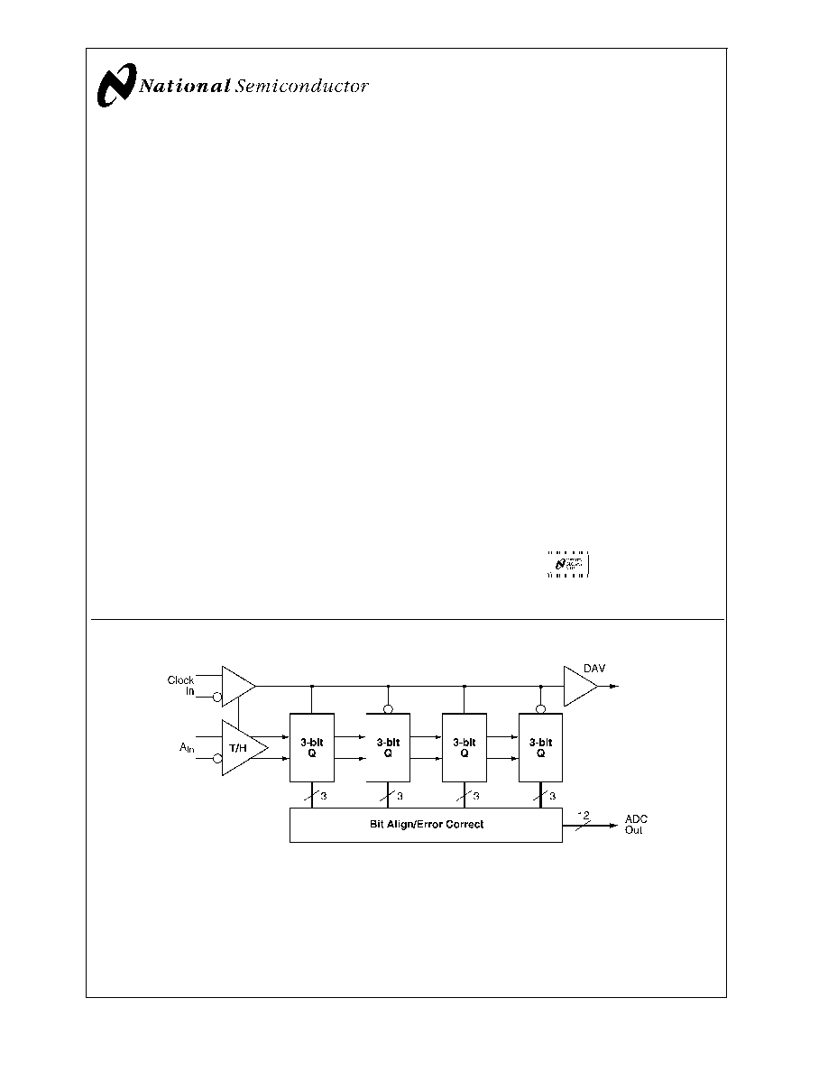
Block Diagram
01502902
April 2002
CLC5957
12-Bit,
70
MSPS
Broadband
Monolithic
A/D
Converter
© 2002 National Semiconductor Corporation
DS015029
www.national.com
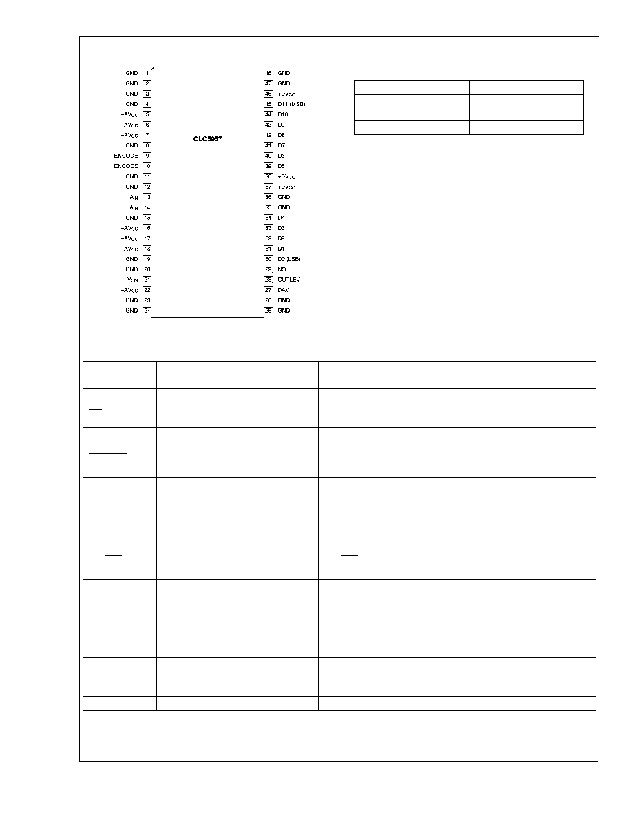
Pin Configuration
01502901
Ordering Information
CLC5957MTD
48-Pin TSSOP
CLC5957MTDX
48-Pin TSSOP (Taped
Reel)
CLC5957PCASM
Evaluation Board
Pin Descriptions
Pin
Name
Pin
No.
Description
A
IN
A
IN
13, 14
Differential input with a common mode voltage of +2.4V. The ADC
full scale input is 1.024 V
PP
on each of the complimentary input
signals.
ENCODE
ENCODE
9, 10
Differential clock where ENCODE initiates a new data conversion
cycle on each rising edge. Logic for these inputs are a 50% duty
cycle universal differential signal (
>
200mV). The clock input is
internally biased to V
CC
/2 with a termination impedance of 2.5k
.
V
CM
21
Internal common mode voltage reference. Nominally +2.4V. Can be
used for the input common mode voltage. This voltage is derived
from an internal bandgap reference. V
CM
should be buffered when
driving any external load. Failure to buffer this signal can cause
errors in the internal bias currents.
D0≠D11
30≠34,
39≠45
Digital data outputs are CMOS and TTL compatible. D0 is the LSB
and D11 is the MSB. MSB is inverted. Output coding is two's
complement. Current limited to source/sink 2.5mA typical.
GND
1≠4, 8, 11, 12, 15, 19,
20, 23≠26, 35, 36, 47, 48
Circuit ground.
+AV
CC
5≠7, 16≠18, 22
+5V power supply for the analog section. Bypass to ground with a
0.1 µF capacitor.
+DV
CC
37, 38, 46
+5V power supply for the digital section. Bypass to ground with a
0.1 µF capacitor.
NC
29
No connect. May be left open or grounded.
DAV
27
Data Valid Clock. Data is valid on rising edge. Current limited to
source/sink 5mA typical.
OUTLEV
28
Output Logic 3.3V or 2.5V option. Open = 3.3V, GND = 2.5V.
CLC5957
www.national.com
2
Absolute Maximum Ratings
(Note 1)
If Military/Aerospace specified devices are required,
please contact the National Semiconductor Sales Office/
Distributors for availability and specifications.
Positive Supply Voltage (V
CC
)
-0.5V to +6V
Differential Voltage between any two
Grounds
<
100 mV
Analog Input Voltage Range
GND to V
CC
Digital Input Voltage Range
-0.5V to +V
CC
Output Short Circuit Duration
(one-pin to ground)
Infinite
Junction Temperature (Note 7)
175∞C
Storage Temperature Range
-65∞C to +150∞C
Lead Solder Duration (+300∞C)
10 sec.
ESD tolerance
human body model
machine model
2000V
200V
Recommended Operating
Conditions
Positive Supply Voltage (V
CC
)
+5V
±
5%
Analog Input Voltage Range
2.048 V
PP
diff.
Operating Temperature Range
-40∞C to +85∞C
Package Thermal Resistance
(Note 7)
Package
JA
JC
48-Pin TSSOP
56∞C/W
16∞C/W
Reliability Information
Transistor Count
5000
Converter Electrical Characteristics
The following specifications apply for AV
CC
= DV
CC
= +5V, 66MSPS. Boldface limits apply for T
A
= T
min
= -40∞C to T
max
=
+85∞C, all other limits T
A
= 25∞C (Note 3).
Symbol
Parameter
Conditions
Min
Typ
Max
Units
DYNAMIC PERFORMANCE
BW
Large-Signal Bandwidth
A
IN
= -3 dBFS
300
MHz
Overvoltage Recovery Time
A
IN
= 1.5 FS (0.01%)
12
ns
t
A
Effective Aperture Delay
-0.41
ns
t
AJ
Aperture Jitter
0.3
ps(rms)
NOISE AND DISTORTION
SNR
*
(Note 2)
Signal-to-Noise Ratio (without 50
harmonics)
f
IN
= 5 MHz, A
IN
= -1dBFS
67
dBFS
f
IN
= 25 MHz, A
IN
= -1dBFS
*
60
66
dBFS
f
IN
= 75 MHz, A
IN
= -3dBFS
65
dBFS
f
IN
= 150 MHz, A
IN
= -15dBFS
66
dBFS
f
IN
= 250 MHz, A
IN
= -15dBFS
66
dBFS
SFDR
Spurious-Free Dynamic Range
f
IN
= 5 MHz, A
IN
= -1dBFS
74
dBc
f
IN
= 25 MHz, A
IN
= -1dBFS
*
60
74
dBc
f
IN
= 75 MHz, A
IN
= -3dBFS
72
dBc
f
IN
= 150 MHz, A
IN
= -15dBFS
69
dBc
f
IN
= 250 MHz, A
IN
= -15dBFS
65
dBc
Spurious-Free Dynamic Range
(dithered)
f
IN
= 19 MHz, A
IN
= -6dBFS
85
dBFS
IMD
Intermodulation Distortion
f
IN1
= 149.84 MHz, f
IN2
= 149.7
MHz, A
IN
= -10dBFS
68
dBFS
f
IN1
= 249.86 MHz, f
IN2
= 249.69
MHz, A
IN
= -10dBFS
58
dBFS
Intermodulation Distortion (dithered)
f
IN1
= 74 MHz, f
IN2
= 75 MHz,
A
IN
= -12dBFS
83
dBFS
DC ACCURACY AND PERFORMANCE
DNL
Differential Non-Linearity
f
IN
= 5MHz, A
IN
= -1dBFS
±
0.65
LSB
INL
Integral Non-Linearity
f
IN
= 5MHz, A
IN
= -1dBFS
±
1.5
LSB
Offset Error (Note 2)
-30
0
30
mV
Gain Error
1.2
% FS
V
REF
Reference Voltage (Note 2)
2.2
2.37
2.6
V
No Missing Codes (Note 2)
f
IN
= 5MHz, A
IN
= -1dBFS
Guaranteed
CLC5957
www.national.com
3

Converter Electrical Characteristics
(Continued)
The following specifications apply for AV
CC
= DV
CC
= +5V, 66MSPS. Boldface limits apply for T
A
= T
min
= -40∞C to T
max
=
+85∞C, all other limits T
A
= 25∞C (Note 3).
Symbol
Parameter
Conditions
Min
Typ
Max
Units
ANALOG INPUTS
V
IN
Analog Diff Input Voltage Range
2.048
V
PP
R
IN
(SE)
Analog Input Resistance
(Single-Ended)
500
R
IN
(Diff)
Analog Input Resistance (Differential)
1000
C
IN
Analog Input Capacitance
(Single-ended)
2
pF
ENCODE INPUTS (UNIVERSAL)
V
IH
Logic Input High Voltage (Note
4),(Note 5)
5
V
V
IL
Logic Input Low Voltage(Note
4),(Note 5)
0
V
Differential Input Swing (Note
4),(Note 5)
0.2
V
DIGITAL OUTPUTS
V
OL
Logic Output Low Voltage (Note 2)
0.01
0.4
V
V
OH
Logic Output High Voltage (Note 2)
OUTLEV = 1 (open)
3.2
3.5
3.8
V
OUTLEV = 0 (GND)
2.4
2.7
3.0
V
TIMING (Note 6)
Maximum Conversion Rate
(ENCODE) (Note 2)
70
75
MSPS
Minimum Conversion Rate
(ENCODE)
10
MSPS
t
P
Pulse Width High (ENCODE) (Note
4)
50% threshold
7.1
ns
t
M
Pulse Width Low (ENCODE) (Note 4) 50% threshold
7.1
ns
t
DNV
ENCODE falling edge to DATA not
valid (Note 4)
8.3
ns
t
DGV
ENCODE falling edge to DATA
guaranteed valid (Note 4)
17.8
ns
t
DAV
Rising ENCODE to rising DAV delay
(Note 4)
50% threshold
8.3
12.6
ns
t
S
DATA setup time before rising DAV
(Note 4)
t
M
-2.4
ns
t
H
DATA hold time after rising DAV
(Note 4)
t
P
-1.6
ns
Pipeline latency
3.0
clk cycle
CLC5957
www.national.com
4

Converter Electrical Characteristics
(Continued)
The following specifications apply for AV
CC
= DV
CC
= +5V, 66MSPS. Boldface limits apply for T
A
= T
min
= -40∞C to T
max
=
+85∞C, all other limits T
A
= 25∞C (Note 3).
Symbol
Parameter
Conditions
Min
Typ
Max
Units
POWER REQUIREMENTS
I
CC
Total Operating Supply Current (Note
2)
128
150
mA
Power Dissipation (Note 2)
640
750
mW
Power Supply Rejection Ratio
64
dB
Note 1: "Absolute Maximum Ratings" are limiting values, to be applied individually, and beyond which the serviceability of the circuit may be impaired. Functional
operability under any of these conditions is not necessarily implied. Exposure to maximum ratings for extended periods may affect device reliability.
Note 2: These parameters are guaranteed by test.
Note 3: Typical specifications are based on the mean test values of deliverable converters from the first three diffusion lots.
Note 4: Values guaranteed based on characterization and simulation.
Note 5: See page 14, Figure 3 for ENCODE inputs circuit.
Note 6: C
L
= 7pF DATA; 10pF DAV.
Note 7: The absolute maximum junction (T
J
max) temperature for this device is 175∞C. The maximum allowable power dissipation is dictated by T
J
max, the
junction-to-ambient thermal resistance (
JA
), and the ambient temperature (T
A
), and can be calculated using the formula P
D
max = (T
J
max ≠ T
A
)/
JA
. For the 48-pin
TSSOP,
JA
is 56∞C/W, so P
D
max = 2.68W at 25∞C and 1.6W at the maximum operating ambient temperature of 85∞C. Note that the power dissipation of this device
under normal operation will typically be about 650 mW (640 mW quiescent power + 10 mW due to 1 TTL load on each digital output). The values of absolute
maximum power dissipation will only be reached when the CLC5957 is operated in a severe fault condition (e.g., when input or output pins are driven beyond the
power supply voltages, or the power supply polarity is reversed). Obviously, such conditions should always be avoided.
CLC5957
www.national.com
5