 | –≠–ª–µ–∫—Ç—Ä–æ–Ω–Ω—ã–π –∫–æ–º–ø–æ–Ω–µ–Ω—Ç: CLC5958 | –°–∫–∞—á–∞—Ç—å:  PDF PDF  ZIP ZIP |
© 1999 National Semiconductor Corporation
http://www.national.com
Printed in the U.S.A.
N
General Description
The CLC5958 is a monolithic 14-bit, 52MSPS analog-to-digital
converter. The ultra-wide dynamic range and high sample rate of
the device make it an excellent choice for wideband receivers
found in multi-channel basestations. The CLC5958 integrates a
low distortion track-and-hold amplifier and a 14-bit multi-stage
quantizer on a single die. Other features include differential
analog inputs, low jitter differential clock inputs, an internal
bandgap voltage reference, and CMOS/TTL compatible outputs.
The CLC5958 is fabricated on the National ABIC-V 0.8 micron
BiCMOS process.
The CLC5958 features a 90dB spurious free dynamic range
(SFDR) and a 70dB signal to noise ratio (SNR). The balanced
differential analog inputs ensure low even-order distortion, while
the differential clock inputs permit the use of balanced clock signals
to minimize clock jitter. The 48-pin CSP package provides an
extremely small footprint for applications where space is a critical
consideration. The package also provides a very low thermal
resistance to ambient. The CLC5958 may be operated with a
single +5V power supply. Alternatively, an additional supply may
be used to program the digital output levels over the range of
+3.3V to +5V. Operation over the industrial temperature range of
-40∞C to +85∞C is guaranteed. National Semiconductor tests
each part to verify compliance with the guaranteed specifications.
CLC5958
14-bit, 52MSPS A/D Converter
Features
∑ 14-bit
∑ 52MSPS
∑ Ultra-wide dynamic range
Noise floor: -72dBFS
SFDR: 90dB
∑ Excellent performance to Nyquist
∑ IF sampling capability
∑ Very small package: 48-pin CSP
∑ Programmable output levels:
3.3V to 5V
Applications
∑ Multi-channel basestations
∑ Multi-standard basestations:
GSM, WCDMA, DAMPS, etc.
∑ Smart antenna systems
∑ Wireless local loop
∑ Wideband digital communications
September 1999
CLC5958
14-bit,
52MSPS A/D Con
ver
ter
Single-Tone Output Spectrum
Power (dBFS)
Frequency (MHz)
0
-20
-120
0
5
25
-40
-60
-80
-100
10
15
20
Sample Rate = 52MSPS
Input Frequency = 5MHz
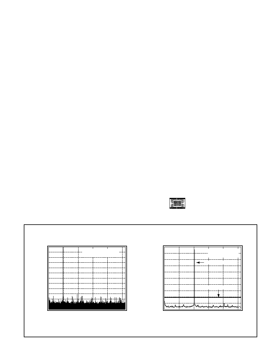
Output Response with GSM 1800 Blocker
Power at the Antenna (dBm)
Frequency (MHz)
-20
-40
-60
-80
-100
-120
0
5
25
10
15
20
Full Scale = -24dBM
Res. BW = 200KHz
-25dBm blocker
-101dBm reference
Actual Size
(Bottom View)
http://www.national.com
2
PARAMETERS
CONDITIONS TEMP
RATINGS
UNITS
NOTES
MIN TYP
MAX
RESOLUTION
Full
14
Bits
1
DIFF. INPUT VOLTAGE RANGE
Full
2.048
V
MAXIMUM CONVERSION RATE
Full
52
65
MSPS
1
SNR
f
in
= 10MHZ, A
in
= -0.6dBFS +25∞C
69
71
dBFS
1
SFDR
f
in
= 10MHZ, A
in
= -0.6dBFS +25∞C
80
90
dB
1
SFDR EXCLUDING 2nd & 3rd HARM.
f
in
= 10MHZ, A
in
= -0.6dBFS +25∞C
85
92
dB
1
NO MISSING CODES
f
in
= 10MHZ, A
in
= -0.6dBFS +25∞C
Guaranteed
1
NOISE AND DISTORTION
noise floor
2
f
in
= 5MHz
A
in
= -1dBFS
+25∞C
-71.0
dBFS
f
in
= 5MHz
A
in
= -20dBFS
+25∞C
-72.0
dBFS
2nd & 3rd harmonic distortion (w/o dither)
f
in
= 5MHz
A
in
= -1dBFS
+25∞C
-90
dBFS
f
in
= 20MHz
A
in
= -1dBFS
+25∞C
-87
dBFS
f
in
= 70MHz
A
in
= -3dBFS
+25∞C
-78
dBFS
next worst harmonic distortion (w/o dither)
3
f
in
= 5MHz
A
in
= -1dBFS
+25∞C
-92
dBFS
f
in
= 20MHz
A
in
= -1dBFS
+25∞C
-90
dBFS
f
in
= 70MHz
A
in
= -3dBFS
+25∞C
-90
dBFS
worst harmonic distortion (with dither)
4
f
in
= 5MHz
A
in
= -6dBFS
+25∞C
-95
dBFS
f
in
= 20MHz
A
in
= -6dBFS
+25∞C
-95
dBFS
f
in
= 70MHz
A
in
= -6dBFS
+25∞C
-82
dBFS
f
in
= 70MHz (2nd & 3rd excluded) A
in
= -6dBFS
+25∞C
-95
dBFS
2-Tone IM distortion (w/o dither)
f
in1
=12MHz, f
in2
= 15MHz
A
in1
= A
in2
= -7dBFS
+25∞C
-100
dBFS
SINAD (w/o dither)
f
in
= 5MHz
A
in
= -1dBFS
+25∞C
69
dB
CLOCK RELATED SPURIOUS TONES
fs/8, fs/4
+25∞C
-95
dBFS
next worst clock spur
+25∞C
-100
dBFS
5
calibration sideband coefficient
+25∞C
100e-6
6
DC ACCURACY AND PERFORMANCE
differential non-linearity
+25∞C
±0.3
LSB
integral non-linearity
+25∞C
±1.5
LSB
offset error
+25∞C
±2.0
mV
gain error
+25∞C
2
% of FS
DYNAMIC PERFORMANCE
large-signal bandwidth
+25∞C
210
MHz
aperture jitter
+25∞C
0.5
ps(rms)
TIMING
effective aperture delay (t
A
)
+25∞C
-0.2
ns
pipeline delay (t
P
)
Full
3
clk cycle
output buffer delay (t
o
)
+25∞C
6.6
ns
data valid buffer delay (t
DAV
)
+25∞C
6.6
ns
ANALOG INPUT CHARACTERISTICS
single-ended input resistance
+25∞C
500
single-ended capacitance
+25∞C
3.6
pF
ENCODE INPUT CHARACTERISTICS
VIH
Full
3.9
4.5
V
7
VIL
Full
3.0
3.8
V
7
differential input swing
Full
0.2
V
IIL
Full
2
µ
A
IIH
Full
25
µ
A
CLC5958 Electrical Characteristics
(V
cc
= +5V, DV
cc
= +3.3V, 52MSPS; unless specified, T
min
= -40∞C, T
max
= +85∞C)
Min/max ratings are based on product characterization and simulation. Individual parameters are tested as noted. Outgoing quality levels are
determined from tested parameters.
3
http://www.national.com
Absolute Maximum Ratings
positive supply voltage
(V
CC
) -0.5V to +6V
differential voltage between any two grounds
<200mV
analog input voltage range
GND to V
CC
digital input voltage range
-0.5V to +V
CC
output short circuit duration (one-pin to ground)
infinite
junction temperature
175∞C
storage temperature range
-65∞C to 150∞C
lead solder duration (+240∞C)
5sec
Note: Absolute maximum ratings are limiting values, to be applied individually, and
beyond which the serviceability of the circuit may be impaired. Functional
operability under any of these conditions is not necessarily implied. Exposure to
maximum ratings for extended periods may affect device reliability.
Recommended Operating Conditions
positive supply voltage (V
CC
)
+5V ±5%
analog input voltage range
2.048V
pp
diff.
input coupling
AC
operating temperature range
-40∞C to +85∞C
digital output supply voltage (DV
CC
)
+3.3V ±5%
analog input common mode voltage
V
cm
±0.025V
Package Thermal Resistance
Package
JA
JC
48-pin CSP
39∞C/W
5∞C/W
Package Transistor Count
Transistor count
10,000
Ordering Information
Model
Temperature Range
Description
CLC5958SLB
-40∞C to +85∞C
48-pin CSP (industrial temperature range)
CLC5958PCASM
Fully loaded evaluation board with CLC5958 ... ready for test.
CLC5958 Timing Diagram
Notes
PARAMETERS
CONDITIONS TEMP
RATINGS
UNITS
NOTES
MIN TYP
MAX
DIGITAL OUTPUT CHARACTERISTICS
VOH
IOH = 50
µ
A
Full
3.2
V
VOL
IOL = 50
µ
A
Full
0.1
V
SUPPLY CHARACTERISTICS
+5V supply current (V
CC
)
+25∞C
260
300
mA
1
+3.3V supply current (DV
CC
)
+25∞C
32
40
mA
1
power dissipation
+25∞C
1.4
W
V
CC
power supply rejection ratio
+25∞C
0.75
mV/V
Min/max ratings are based on product characterization and simulation. Individual parameters are tested as noted. Outgoing quality levels are
determined from tested parameters.
CLC5958 Electrical Characteristics
(V
cc
= +5V, DV
cc
= +3.3V, 52MSPS; unless specified, T
min
= -40∞C, T
max
= +85∞C)
1) These parameters are 100% tested at 25∞C.
2) Harmonics and clock spurious are removed in noise
measurements.
3) 4th or higher harmonic.
4) Low frequency dither injected in the DC to 500KHz band.
5) Next worst clock spur is a subharmonic of fs, but not fs/8 or fs/4.
See text on spurious.
6) See text on calibration sidebands in the application
information section.
7) Encode levels are referenced to V
CC
, i.e. the minimum VIH value is
1.1V below V
CC
, and the maximum VIH value is 0.5V below V
CC
.
N-3
N-2
N-1
N
N
N+1
N+2
N+3
t
A
Analog
Input
ENCODE
Data
DAV
t
O
t
DAV
N + 1
t
O
:
Delay from rising edge of
ENCODE to output data
transition ≠ nominally 6.6ns
t
DAV
: Delay from falling edge of
ENCODE to rising edge of DAV
≠ nominally 6.6ns
t
A
:
Effective aperture delay
≠ nominally -0.2ns
CLC5958 Timing Diagram
http://www.national.com
4
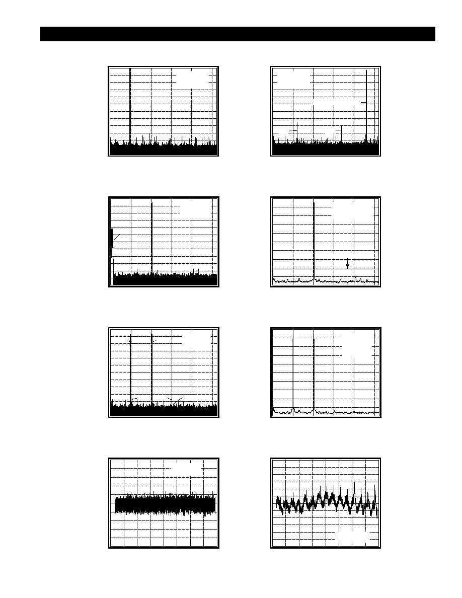
Single-Tone Output Spectrum
w/200KHz Res. BW
Power at the Antenna (dBm)
Frequency (MHz)
-20
-40
-60
-80
-100
Single-Tone Output Spectrum
Power (dBFS)
Frequency (MHz)
0
-20
-40
-60
-80
-100
Single-Tone Output Spectrum (w/Dither)
Power (dBFS)
Frequency (MHz)
0
-20
-40
-60
-80
-100
Dither
Differential Non-Linearity
LSBs
Code
F
s
= 52MSPS
F
in
= 4.9791
0
4000
8000
12000
16000
-1.0
-0.6
-0.2
0.2
0.6
1.0
Integral Non-Linearity
LSBs
Code
3.0
-3.0
0
4000
8000
1.0
0
-2.0
12000
16000
F
s
= 52MSPS
F
in
= 4.9791MHz
2.0
-1.0
Single-Tone Output Spectrum
Power (dBFS)
Frequency (MHz)
0
-20
-40
-60
-80
-100
Two-Tone Output Spec. w/200KHz Res. BW
Power at the Antenna (dBm)
Frequency (MHz)
-20
-40
-60
-80
-100
Two-Tone Output Spectrum
Power (dBFS)
Frequency (MHz)
0
-20
-60
-80
-100
f2
f1
f2-f1
f1+f2
-40
-120
0
5
25
10
15
20
F
s
= 52MSPS
F
in
= 5MHz
A
in
= -0.6dBFS
-120
0
5
25
10
15
20
2nd
3rd
Fundamental = 75MHz
F
s
= 52MSPS
F
in
= 75MHz
A
in
= -3.2dBFS
-120
0
5
25
10
15
20
F
s
= 52MSPS
F
in
= 10MHz
A
in
= -6dBFS
-120
0
5
25
10
15
20
F
s
= 52MSPS
f
1
= 5MHz
f
2
= 10MHz
2f2-f1
-120
0
5
25
10
15
20
F
in1
= 5MHz
F
in2
= 10MHz
A
in1
= -31dBm
A
in2
= -31dBm
-120
0
5
25
10
15
20
Full Scale = -24dBm
F
in
= 10MHz
A
in
= -25dBm
-101dBm reference
CLC5958 Typical Performance Characteristics
(V
cc
= +5V, 52MSPS; unless specified)
5
http://www.national.com
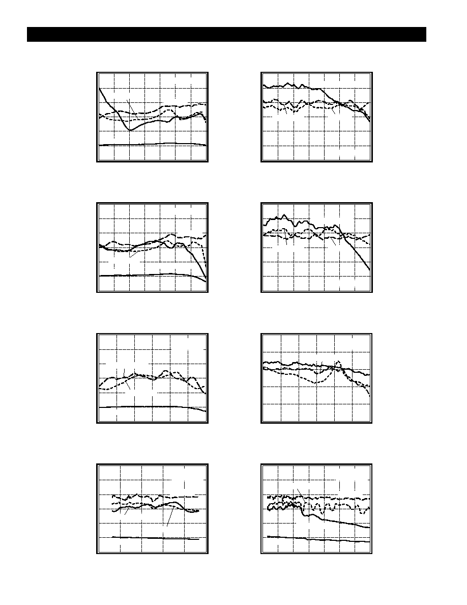
CLC5958 Typical Performance Characteristics
(V
cc
= +5V, 52MSPS; unless specified)
2nd or 3rd Harmonic
Noise and Spurious
vs. Amplitude at F
in
= 10MHz
-dBFS
Amplitude (dBFS)
60
-70
-60
-50
-40
-30
-20
-10
0
120
110
F
s
= 52MSPS
90
80
Other Spurious
Noise Floor
70
Clock Spurious vs. Sample Rate
-dBFS
Sample Rate (MSPS)
120
110
70
10
20
30
40
50
60
70
100
F
in
= 10MHz
A
in
= -0.6dBFS
90
80
"next clock spurs"
fs/4
fs/8
100
F
s
/8 or F
s
/4
Spurious vs. Amplitude
with Dither at F
in
= 10MHz
-dBFS
Amplitude (dBFS)
60
-70
-60
-50
-40
-30
-20
-10
0
120
110
F
s
= 52MSPS
90
80
Other Spurious
70
100
F
s
/8 or F
s
/4
Noise and Spurious
vs. Amplitude at F
in
= 75MHz
-dBFS
Amplitude (dBFS)
60
-70
-60
-50
-40
-30
-20
-10
0
120
110
F
s
= 52MSPS
90
80
Other Spurious
Noise Floor
70
100
F
s
/8 or F
s
/4
Spurious vs. Amplitude
with Dither at F
in
= 75MHz
-dBFS
Amplitude (dBFS)
60
-70
-60
-50
-40
-30
-20
-10
0
120
110
F
s
= 52MSPS
90
80
Other Spurious
70
100
F
s
/8 or F
s
/4
2nd or 3rd Harmonic
2nd or 3rd Harmonic
Noise and Distortion vs. Sample Rate
dBFS
Sample Rate (MSPS)
120
110
60
10
20
30
40
50
60
70
90
80
70
100
Noise and Spurious vs. Input Frequency
-dBFS
120
110
60
0
5
10
15
20
25
90
80
70
100
Noise and Spurious vs. Input Frequency
-dBFS
Input Frequency (MHz)
Input Frequency (MHz)
120
110
60
0
10
30
40
50
60
70
90
80
70
100
F
s
= 52MSPS
A
in
= -0.6dBFS
Other Spurious
Noise Floor
F
s
/8 or F
s
/4
2nd or 3rd Harmonic
20
Noise Floor
F
s
/8 or F
s
/4
2nd or 3rd Harmonic
Other Spurious
2nd or 3rd Harmonic
F
s
= 52MSPS
A
in
= -3.2dBFS
F
in
= 10MHz
A
in
= -0.6dBFS
Other Spurious
Noise Floor
2nd or 3rd Harmonic