 | –≠–ª–µ–∫—Ç—Ä–æ–Ω–Ω—ã–π –∫–æ–º–ø–æ–Ω–µ–Ω—Ç: CLC730019 | –°–∫–∞—á–∞—Ç—å:  PDF PDF  ZIP ZIP |
CLC5665
Low Distortion Amplifier with Disable
General Description
The CLC5665 is a low cost, wideband amplifier that provides
very low 2nd and 3rd harmonic distortion at 1MHz
(-89/-92dBc). The great slew rate of 1800V/µs, bandwidth
of 90MHz (A
V
= +1) and fast disable make it an excellent
choice for many high speed multiplexing applications. Like
all current feedback op amps, the CLC5665 allows the fre-
quency response to be optimized (or adjusted) by the selec-
tion of the feedback resistor. For demanding video applica-
tions, the 0.1 dB bandwidth to 20MHz and differential
gain/phase of 0.05%/0.05∞ make the CLC5665 the preferred
component for broadcast quality NTSC and PAL video sys-
tems.
The large voltage swing (28V
PP
) , continuous output current
(85mA) and slew rate (1800V/µs) provide high fidelity signal
conditioning for applications such as CCDs, transmission
lines and low impedance circuits.
xDSL, video distribution, multimedia and general purpose
applications will benefit from the CLC5665's wide bandwidth
and disable feature. Power is reduced and the output be-
comes a high impedance when disabled. The wide gain
range of the CLC5665 makes this general purpose op amp
an improved solution for circuits such as active filters,
differential-to-single-ended drivers, DAC transimpedance
amplifiers and MOSFET drivers.
Features
n
0.1dB gain flatness to 20MHz (A
V
= +2)
n
90MHz bandwidth (A
V
= +1)
n
Large signal BW 25MHz
n
1800V/µs slew rate
n
0.05%/0.05∞ differential gain/phase
n
±
5V,
±
15V or single supplies
n
200ns disable to high impedance output
n
Wide gain range
n
-89/-92dBc HD2/HD3 (R
L
=500
)
n
Low cost
Applications
n
xDSL driver
n
Twisted pair driver
n
Cable driver
n
Video distribution
n
CCD clock driver
n
Multimedia systems
n
DAC output buffers
n
Imaging systems
Connection Diagram
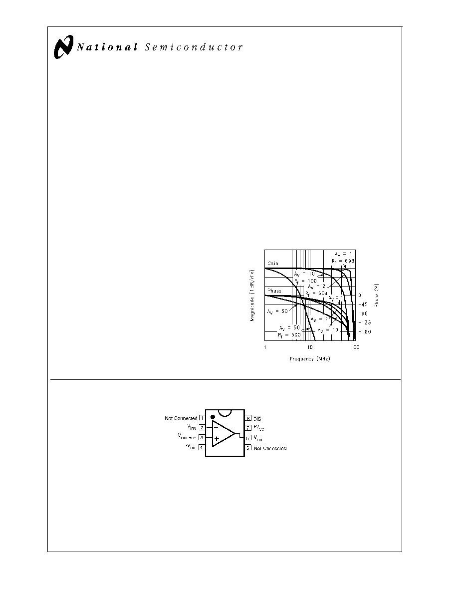
Non-Inverting Frequency Response
DS015015-1
DS015015-3
Pinout
DIP & SOIC
December 2000
CLC5665
Low
Distortion
Amplifier
with
Disable
© 2000 National Semiconductor Corporation
DS015015
www.national.com
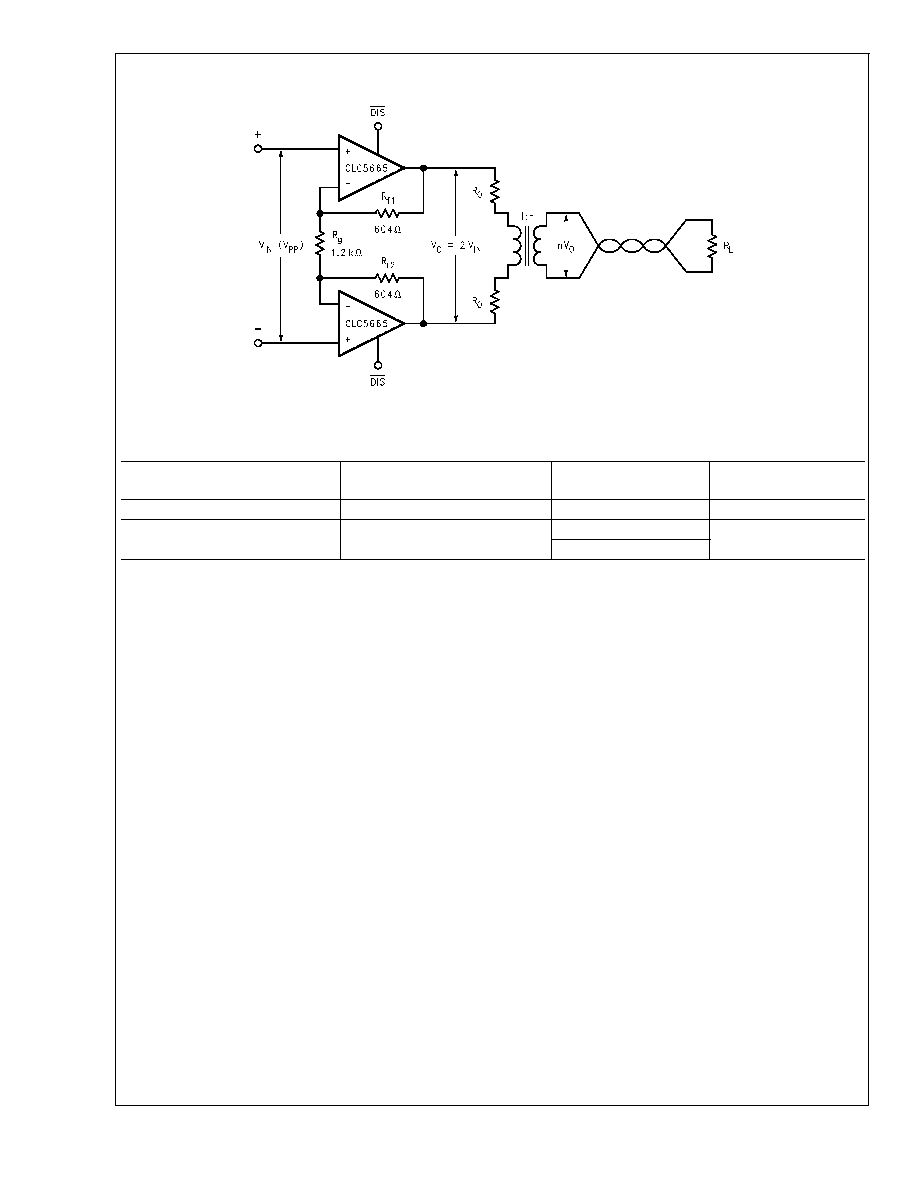
Typical Application
Ordering Information
Package
Temperature Range
Industrial
Packaging
Marking
NSC
Drawing
8-pin plastic DIP
-40∞C to +85∞C
CLC5665IN
N08E
8-pin plastic SOIC
-40∞C to +85∞C
CLC5665IM
M08A
CLC5665IMX
DS015015-2
Differential Line Driver for xDSL
CLC5665
www.national.com
2
Absolute Maximum Ratings
(Note 1)
If Military/Aerospace specified devices are required,
please contact the National Semiconductor Sales Office/
Distributors for availability and specifications.
Supply Voltage
±
16V
Short Circuit Current
(see (Note 4))
Common-Mode Input Voltage
±
V
CC
Maximum Junction Temperature
+150∞C
Storage Temperature Range
-65∞C to +150∞C
Lead Temperature (soldering 10 sec)
+300∞C
Operating Ratings
Thermal Resistance
Package
(
JC
)
(
JA
)
MDIP
65∞C/W
130∞C/W
SOIC
50∞C/W
145∞C/W
Electrical Characteristics
V
CC
=
±
15V, A
V
= +2V/V; R
f
=604
, R
L
=100
; unless specified
Symbol
Parameter
Conditions
V
CC
Typ
Min/Max Ratings
(Note 2)
Units
Ambient Temperature
CLC5665IN/IM
+25∞C
+25∞C
0 to
70∞C
-40 to
85∞C
Frequency Domain Response
Small-Signal Bandwidth
(A
V
= +1)
V
OUT
<
1.0V
PP
±
15
90
MHz
Small-Signal Bandwidth
V
OUT
<
1.0V
PP
±
15
70
MHz
V
OUT
<
1.0V
PP
±
5
50
MHz
0.1dB Bandwidth
V
OUT
<
1.0V
PP
±
15
20
MHz
V
OUT
<
1.0V
PP
±
5
15
MHz
Large-Signal Bandwidth
V
OUT
<
10V
PP
25
MHz
Gain Flatness
V
OUT
<
1.0V
PP
Peaking
DC to 10MHz
0.03
dB
Rolloff
DC to 20MHz
0.1
dB
Linear Phase Deviation
DC to 20MHz
0.7
deg
Differential Gain
R
L
= 150
, 4.43MHz
±
15
0.05
%
R
L
= 150
, 4.43MHz
±
5
0.05
%
Differential Phase
R
L
= 150
, 4.43MHz
±
15
0.05
deg
R
L
= 150
, 4.43MHz
±
5
0.1
deg
Time Domain Response
Rise and Fall Time
2V Step
5
ns
10V Step
10
ns
Settling Time to 0.05%
2V Step
35
ns
Overshoot
2V Step
5
%
Slew Rate
20V Step
1800
V/µs
Distortion And Noise Response
2nd Harmonic DIstortion
1V
PP
,1MHz,
R
L
= 500
-89
dBc
3rd Harmonic Distortion
2V
PP
,1MHz,
R
L
= 500
-92
dBc
Input Voltage Noise
>
1MHz
3.0
nV/
Non-Inverting Input Current
Noise
>
1MHz
3.2
pA/
Inverting Input Current
Noise
>
1MHz
15
pA/
DC Performance
Input Offset Voltage
(Note 3)
±
15
1.0
7.5
9.0
10.0
mV
Average Drift
25
µV/∞C
CLC5665
www.national.com
3
Electrical Characteristics
(Continued)
V
CC
=
±
15V, A
V
= +2V/V; R
f
=604
, R
L
=100
; unless specified
Symbol
Parameter
Conditions
V
CC
Typ
Min/Max Ratings
(Note 2)
Units
DC Performance
Input Bias Current
(Note 3)
Non-Inverting
±
15,
±
5
3
20
20
20
µA
Average Drift
10
nA/∞C
Input Bias Current
(Note 3)
Inverting
±
15,
±
5
3
20
20
20
µA
Average Drift
10
nA/∞C
Power Supply Rejection
Ratio
DC
60
55
50
50
dB
Common-Mode Rejection
Ratio
DC
60
55
50
50
dB
Supply Current (Note 3)
R
L
=
±
15,
±
5
11,8.5
12
14
15
mA
Disabled (Note 3)
R
L
=
±
15,
±
5
1.5
2.5
2.5
2.5
mA
Switching Performance
Turn on Time
400
500
550
550
ns
Turn Off Time
(Note 5)
200
800
800
800
ns
Off Isolation
10MHz
59
56
56
56
dB
High Input Voltage
V
IH
±
15
11.8
12.5
12.7
V
±
5
1.8
2.5
2.7
V
Low Input Voltage
V
IL
±
15
10.8
10.5
10.0
V
±
5
0.8
0.6
0.1
V
Miscellaneous Performance
Non-Inverting Input
Resistance
8.0
3.0
2.5
1.7
M
Non-Inverting Input
Capacitance
0.5
1.0
1.0
1.0
pF
Input Voltage Range
Common Mode
±
15
±
12.5
±
12.3
±
12.1
±
11.8
Common Mode
±
5
±
2.5
±
2.3
±
2.2
±
1.9
V
Output Voltage Range
R
L
=
±
15
±
14
±
13.7
±
13.7
±
13.6
V
R
L
=
±
5
±
4.0
±
3.9
±
3.8
±
3.7
V
Output Current
±
85
±
60
±
50
±
45
mA
Note 1: "Absolute Maximum Ratings" are those values beyond which the safety of the device cannot be guaranteed. They are not meant to imply that the devices
should be operated at these limits. The table of "Electrical Characteristics" specifies conditions of device operation.
Note 2: Min/max ratings are based on product characterization and simulation. Individual parameters are tested as noted. Outgoing quality levels are determined
from tested parameters.
Note 3: AJ-level: spec. is 100% tested at +25∞C.
Note 4: Output is short circuit protected to ground, however maximum reliability is obtained if output current does not exceed 125mA.
Note 5: To
>
50dB attenuation
@
10MHz.
CLC5665
www.national.com
4
Typical Performance Characteristics
(V
CC
=
±
15V, A
V
= +2V/V; R
f
= 604
, R
L
= 100;
unless
specified)
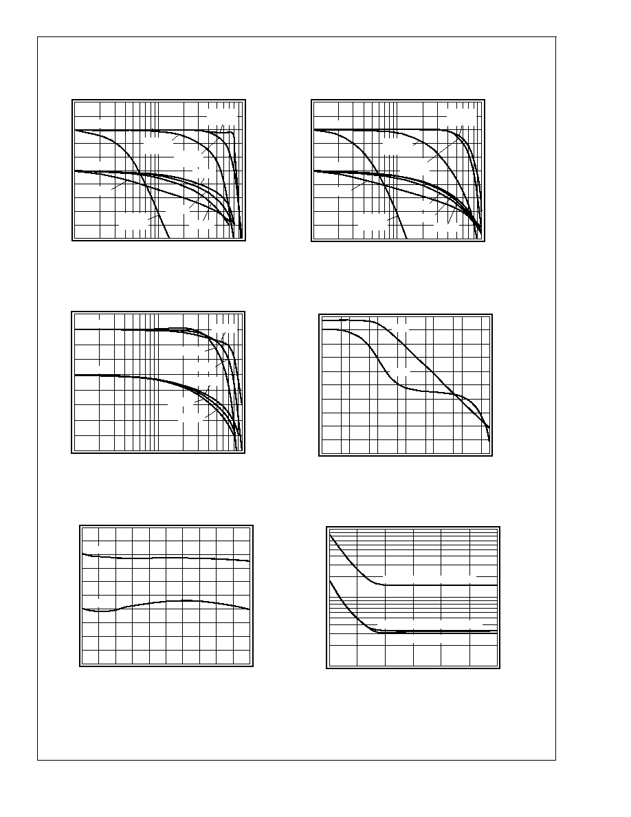
Non-Inverting Frequency Response
Magnitude (1dB/div)
Frequency (MHz)
1
10
100
Gain
Phase (deg)
-90
0
-180
-45
-135
Phase
A
v
= 2
R
f
= 604
A
v
= 1
R
f
= 698
A
v
= 10
R
f
= 100
A
v
= 50
R
f
= 500
A
v
= 1
A
v
= 2
A
v
= 10
A
v
= 50
DS015015-4
Inverting Frequency Response
Magnitude (1dB/div)
Frequency (MHz)
1
10
100
Gain
Phase (deg)
-90
0
-180
-45
-135
Phase
A
v
= -2
R
f
= 500
A
v
= -1
R
f
= 500
A
v
= -10
R
f
= 500
A
v
= -50
R
f
= 2.5k
A
v
= -10
A
v
= -2
A
v
= -1
A
v
= -50
DS015015-5
Frequency Response vs. Load
Magnitude (1dB/div)
Frequency (MHz)
1
10
100
Gain
Phase (deg)
-90
0
-180
-45
-135
Phase
R
L
= 1k
R
L
= 100
R
L
= 50
R
L
= 1k
R
L
= 100
R
L
= 50
DS015015-6
Open-Loop Transimpedance Gain (Zs)
Gain (20 log)
Frequency (MHz)
0.0001
0.001
0.01
1
10
0.1
100
Gain
Phase (deg)
120
160
100
140
40
80
20
60
0
60
40
30
70
50
100
80
110
90
120
130
Phase
DS015015-7
Flatness Gain and Linear Phase
Magnitude (0.1dB/div)
Frequency (MHz)
0
4
8
12
16
20
Gain
Phase (0.2
/div)
Phase
DS015015-8
Equivalent Input Noise
Noise Voltage (nV/
Hz)
Frequency (MHz)
0.1k
1k
10k
100k
1M
100M
Inverting Current 14.8pA/
Hz
Noise Current (pA/
Hz)
Non-Inverting Current 3.2pA/
Hz
Voltage 3.0nV/
Hz
10M
1
10
100
DS015015-9
CLC5665
www.national.com
5