The CLC730024 is an evaluation board intended for the
evaluation of quad Op-Amps in the DIP package. The
CLC730031 is a similar board, but laid out for an SOIC
package.
To obtain optimum performance from a high speed
device, a good Printed Circuit Board (PCB) layout
is essential. The importance of the layout becomes
greater as the frequency of operation increases. Some
of National Semiconductor's quad Op-Amps have
bandwidths in excess of 100MHZ, therefore it is vital that
sound PCB layout techniques be used when designing
with these devices. The CLC730024 and CLC730031
are examples of good PCB layouts which designers are
encouraged to copy.
To minimize capacitive feedthrough and noise, if there
are op-amps not being used, they should be configured
as unity gain buffers (with a resistor in the feedback path
for current feedback devices) and the non-inverting
inputs connected to GND. On devices that are being
used, the ground plane should be removed from beneath
the feedback and gain setting resistors, to minimize
parasitic capacitance on sensitive nodes. Input and out-
put traces should be laid out as transmission lines with
the appropriate termination resistors very near the
device. On a 0.0065" (FR4 or equivalent) a 0.1" wide
trace over ground plane on the opposite side of the board
will exhibit a characteristic impedance of 50
.
Parasitic or load capacitance directly on the output of
an amplifier will introduce additional phase shift in the
device. If excessive, this phase shift can lead to peaking
in the frequency response or, in extreme cases, oscilla-
tion. A small series resistor in series with a capacitive
load effectively decouples it from the buffer output and
removes the undesirable effects of excess phase shift.
Further detail on the selection of these resistors can be
found in the individual amplifier data sheets.
Parts List
R
IN1
, R
IN2
, R
IN3
, R
IN4
,
select for desired input resistance
R
OUT1
,R
OUT2
,R
OUT3
, R
OUT4
select for desired output resistance
R
F1
,R
F2
,R
F3
,R
F4
select according to data sheet and application
R
G1
,R
G2
,R
G3
,R
G4
select according to data sheet and application
C
1
,C
2
0.1
�
F capacitor
C
3
,C
4
6.8
�
F capacitor
L
1
,L
2
Optional ferrite bead inductors
Quad Op Amp Evaluation Boards
Part Number CLC730024, CLC730031
August 1997
� 1997 National Semiconductor Corporation
http://www.national.com
Printed in the U.S.A.
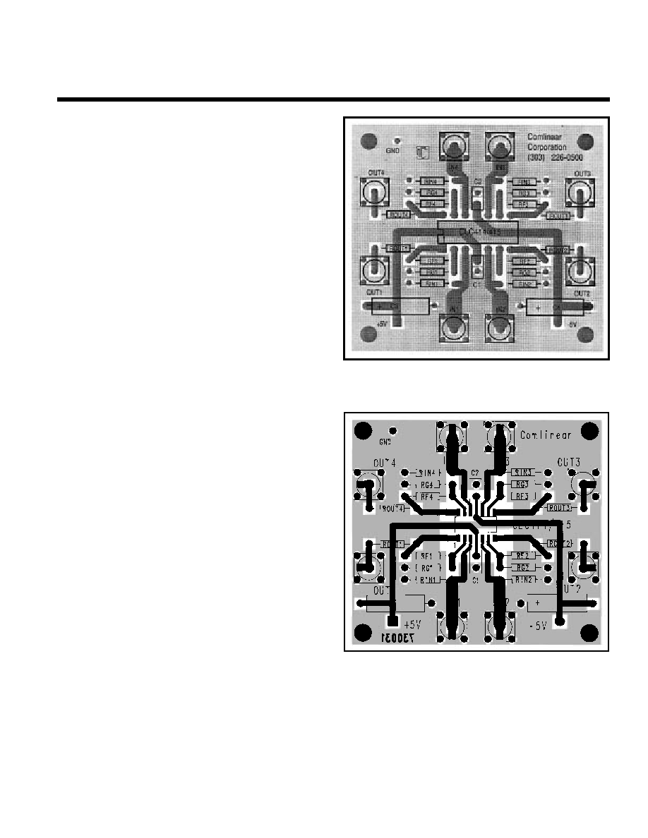
N
Figure 1: 730024 Board Layout and
Component Placement
Figure 2: 730031 Board Layout and
Component Placement
http://www.national.com
2
Lit #660414-002
Customer Design Applications Support
National Semiconductor is committed to design excellence. For sales, literature and technical support, call the National
Semiconductor Customer Response Group at 1-800-272-9959 or fax 1-800-737-7018.
Life Support Policy
National's products are not authorized for use as critical components in life support devices or systems without the express written approval of the
president of National Semiconductor Corporation. As used herein:
1. Life support devices or systems are devices or systems which, a) are intended for surgical implant into the body, or b) support or
sustain life, and whose failure to perform, when properly used in accordance with instructions for use provided in the labeling, can
be reasonably expected to result in a significant injury to the user.
2. A critical component is any component of a life support device or system whose failure to perform can be reasonably expected to
cause the failure of the life support device or system, or to affect its safety or effectiveness.
National Semiconductor
National Semiconductor
National Semiconductor
National Semiconductor
Corporation
Europe
Hong Kong Ltd.
Japan Ltd.
1111 West Bardin Road
Fax: (+49) 0-180-530 85 86
13th Floor, Straight Block
Tel: 81-043-299-2309
Arlington, TX 76017
E-mail: europe.support.nsc.com
Ocean Centre, 5 Canton Road
Fax: 81-043-299-2408
Tel: 1(800) 272-9959
Deutsch Tel: (+49) 0-180-530 85 85
Tsimshatsui, Kowloon
Fax: 1(800) 737-7018
English Tel: (+49) 0-180-532 78 32
Hong Kong
Francais Tel: (+49) 0-180-532 93 58
Tel: (852) 2737-1600
Italiano Tel: (+49) 0-180-534 16 80
Fax: (852) 2736-9960
National does not assume any responsibility for use of any circuitry described, no circuit patent licenses are implied and National reserves the right at any time without notice to change said
circuitry and specifications.
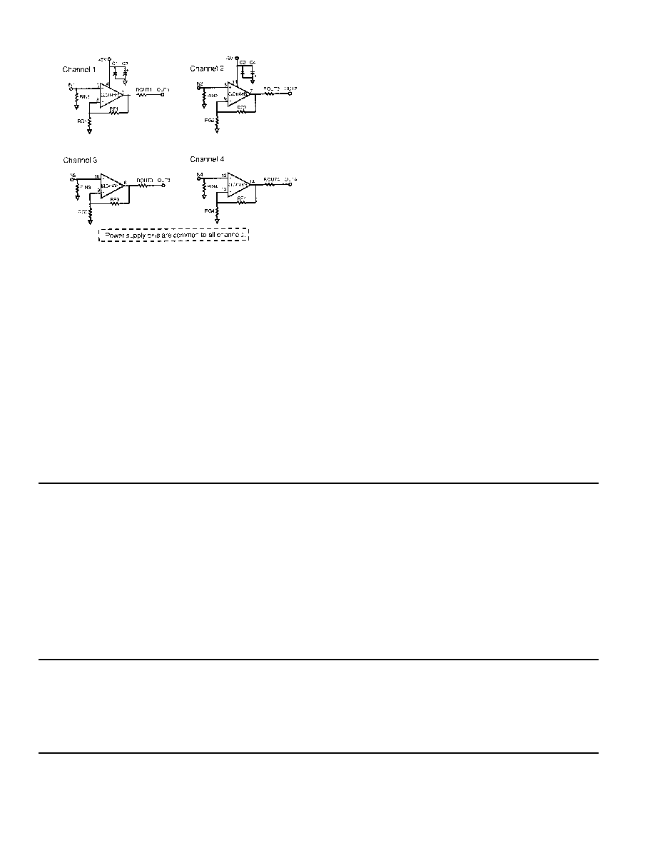
N
Figure 3: Evaluation Board Schematic