 | –≠–ª–µ–∫—Ç—Ä–æ–Ω–Ω—ã–π –∫–æ–º–ø–æ–Ω–µ–Ω—Ç: CLC949A | –°–∫–∞—á–∞—Ç—å:  PDF PDF  ZIP ZIP |
SFDR (dBc)
SNR (dB), SFDR (dBc)
Power Dissipation vs. Conversion Rate
200
150
100
50
0
Power (mW)
0
5
10
15
20
Sample Rate (MSPS)
Features
s
Very low/programmable power
0.07W @ 5MSPS
0.22W @ 20MSPS
0.40W @ 30MSPS
s
Single supply operation (+5V)
s
0.5 LSB differential linearity error
s
Wide dynamic range
72dBc spurious-free dynamic range
68dB signal-to-noise ratio
s
No missing codes
Applications
s
CCD imaging
s
IR imaging
s
FLIR processing
s
Medical imaging
s
High definition video
s
Instrumentation
s
Radar processing
s
Digital communications
General Description
The Comlinear CLC949 is a 12-bit analog-to-digital converter sub-
system including 12-bit quantizer, sample-and-hold amplifier, and
internal reference. The CLC949 has been optimized for low power
operation with high dynamic range. The CLC949 has a unique
feature which allows the user to adjust internal bias levels in the
converter which results in a trade-off between power dissipation
and maximum conversion rate. With bias set for 220mW power
dissipation the converter operates at 20MSPS. Under these
conditions, dynamic performance with a 9.9MHz analog input is
typically 68dB SNR and 72dBc SFDR. When bias is set for only
65mW power dissipation the converter maintains excellent perfor-
mance at 5MSPS. With a 2.4MHz analog input signal the SNR is
70dB and SFDR is 78dBc. This excellent dynamic performance in
the frequency domain without high power requirements make the
part a strong performer for communications and radar applications.
The low input noise of the CLC949, its 0.5LSB differential linearity
error specification, fast settling, and low power dissipation also
lead to excellent performance in imaging systems. All parts are
thoroughly tested to insure that guaranteed specifications are met.
The CLC949 incorporates an input sample-and-hold amplifier
followed by a quantizer which uses a pipelined architecture to min-
imize comparator count and the associated power dissipation
penalty. An on-board voltage reference is provided. Analog input
signals, conversion clock, and a single supply are all that are
required for CLC949 operation.
The CLC949 exhibits very stable performance over the commercial
and industrial temperature ranges. Most parameters shift very
little as the ambient temperature changes from -40∞C to 85∞C. An
exception to this rule is the dynamic performance of the converter.
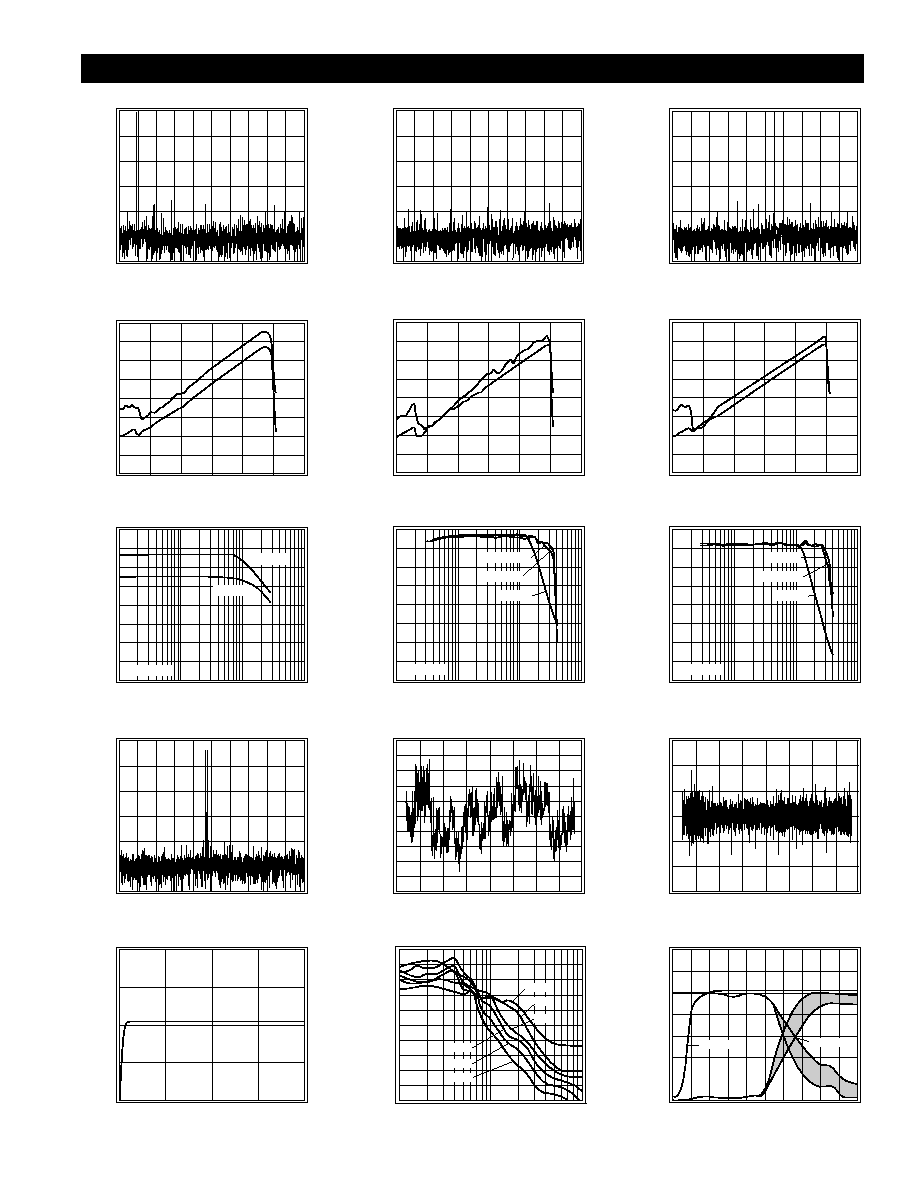
As the temperature is increased, the distortion increases,
especially at higher input frequencies. This can be seen in the plot
on page 3. For input frequencies below 7MHz, there is relatively
little variation in distortion as the temperature is changed, but at
higher input frequencies, it is apparent that the performance
degrades as the temperature is increased.
Note that the reason for this degradation is the reduced ability of
the CLC949 to handle high slew rates at high temperatures. In
applications such as CCD imaging systems, where the slew rate at
the A/D sampling instant is very low, this degradation will not be
nearly so pronounced.
For applications requiring high temperature operation and very low
distortion with high frequency input signals, use of an external
sample-and-hold amplifier may enhance performance by reducing
the slew rates that the CLC949 sees during its sampling period (just
after the falling edge of CLK).
The CLC949 is fabricated in a 0.9
µ
m CMOS technology. The
CLC949ACQ is specified over the commercial temperature range
of 0∞C to +70∞C and the CLC949AJQ is specified over the indus-
trial range of -40∞C to +85∞C. Both are packaged in a 44-pin
Plastic Leaded Chip Carrier (PLCC)
.
Comlinear CLC949
Very Low-Power, 12-Bit,
20MSPS Monolithic A/D Convertter
N
August 1996
Comlinear CLC949
V
ery Low-Power
, 12-Bit, 20MSPS Monolithic Converter
© 1996 National Semiconductor Corporation
http://www.national.com
Printed in the U.S.A.
http://www.national.com
2
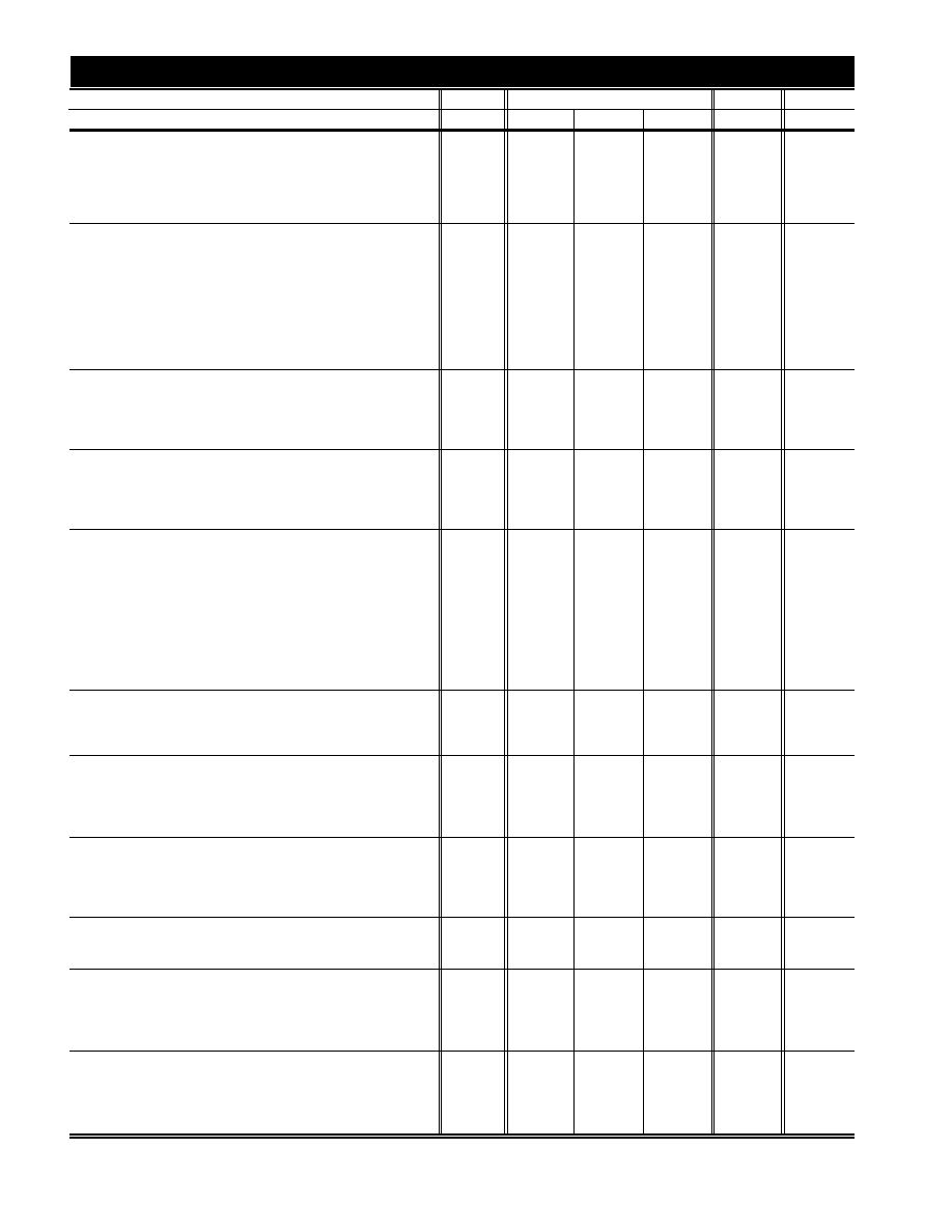
PARAMETERS
CONDITIONS
TYP
MIN/MAX RATINGS
UNITS SYMBOL
Case Temperature
+25∞C
0 to 70∞C -40 to 85∞C
DYNAMIC CHARACTERISTICS
overvoltage recovery V
IN
= 1.5FS
15
25
25
25
ns
OR
effective aperture delay
3.0
6.2
6.2
6.2
ns
TA
aperture jitter
7.0
15
15
15
ps(rms)
AJ
slew rate
400
V/
µ
S
SR
settling time
12
ns
ST
NOISE and DISTORTION (20MSPS)
Signal-to-Noise Ratio (no harmonics)
4.985MHz;
FS
68
66
66
66
dB
SNR2
9.663MHz;
FS
68
66
66
66
dB
SNR3
Spurious-Free Dynamic Range
4.985MHz;
FS -1dB
72
dBc
SFDR2
9.663MHz;
FS -1dB
72
63
58
55
dBc
SFDR3
Intermodulation Distortion
f
1
= 5.58MHz @ FS -7dB; f
2
= 5.70MHz @ FS -7dB
-70
dBc
IMD
3dB bandwidth (full power)
100
MHz
BW
NOISE and DISTORTION (5MSPS, low bias)
Signal-to-Noise Ratio (no harmonics)
2.4MHz;
FS
70
68
68
67
dB
SNR1
Spurious-Free Dynamic Range
2.4MHz;
FS -1dB
78
66
66
64
dBc
SFDR1
NOISE and DISTORTION (25.6MSPS, high bias)
Signal-to-Noise Ratio (no harmonics)
9.894MHz;
FS
67
63
63
63
dB
SNR4
Spurious-Free Dynamic Range
9.894MHz;
FS-1dB
67
59
53
48
dBc
SFDR4
DC ACCURACY and PERFORMANCE
differential non-linearity
dc; FS
0.5
1.0
1.0
1.0
LSB
DNL
integral non-linearity
dc; FS
1.2
3.5
3.5
3.5
LSB
INL
common mode rejection ratio
dc
60
dB
CMRR
missing codes
0
0
0
0
codes
MC
mid-scale offset
5.0
25
25
25
mV
VIO
temperature coefficient
15
µ
V/∞C
DVIO
gain error
1.0
5.0
5.0
5.0
%FS
GE
power supply rejection
V
dda
dc
55
dB
PSRA
V
ddd
dc
50
dB
PSRD
VOLTAGE REFERENCE CHARACTERISTICS
positive reference voltage (internal)
3.25
3.24-3.26
3.24-3.26
3.24-3.26
V
VREFP
negative reference voltage (internal)
1.25
1.24-1.26
1.24-1.26
1.24-1.26
V
VREFN
differential reference voltage (Vrefp - Vrefn)
2.0
1.98-2.02
1.98-2.02
1.98-2.02
V
VDIFF
ANALOG INPUT PERFORMANCE
common mode range
2 - 3
V
VCM
differential range
± 2
V
VDM
analog input bias current
±0.1
±1.0
±1.0
±1.0
µ
A
IBN
analog input capacitance
5.0
10
10
10
pF
CIN
DIGITAL INPUTS
CMOS input voltage
logic LOW
1
1
1
V
VIL
logic HIGH
4.0
4.0
4.0
V
VIH
CMOS input current
logic LOW
±0.1
±1.0
±1.0
±1.0
µ
A
IIL
logic HIGH
±0.1
±1.0
±1.0
±1.0
µ
A
IIH
DIGITAL OUTPUTS
CMOS output voltage
logic LOW
0.25
0.5
0.5
0.5
V
VOL
logic HIGH
4.8
4.5
4.5
4.5
V
VOH
TIMING
maximum conversion rate
30
30
30
30
MSPS
CR
minimum conversion rate
10
10
10
10
KSPS
CRM
data hold time
7.0
4.5
4.5
4.5
ns
THLD
pipeline delay
6.5
6.5
6.5
6.5
clocks
POWER REQUIREMENTS
supply current (+V
dd
)
44
60
60
60
mA
IDD
power dissipation
20MSPS
220
300
300
300
mW
PDM
power dissipation (low bias)
5MSPS
65
mW
PDL
power dissipation (high bias)
30MSPS
400
mW
PDH
Min/max ratings are based on product characterization and simulation. Individual parameters are tested as noted. Outgoing quality levels
are determined from tested parameters.
CLC949 Electrical Characteristics
(+V
DD
= + 5V, Medium Bias (200
µ
A): unless specified)
3
http://www.national.com
CLC949 Typical Performance Characteristics
(+V
DD
= + 5V, Med Bias, F
s
= 20MSPS: unless specified)
Output Spectrum 1MHz
Output Level (dBFS)
Frequency (MHz)
0
-40
0
2
4
-120
-80
10
6
8
-20
-60
-100
Output Spectrum 9MHz
Output Level (dBFS)
Frequency (MHz)
0
-40
0
2
4
-120
-80
10
6
8
-20
-60
-100
Output Spectrum 15MHz
Output Level (dBFS)
Frequency (MHz)
0
-40
0
2
4
-120
-80
10
6
8
-20
-60
-100
SNR & SFDR vs. Input Amplitude 1MHz
SNR (dB) & SFDR (dBc)
Input Amplitude (dBFS)
80
60
-50
-30
-10
20
0
40
SNR
SFDR
10
-40
-20
0
SNR & SFDR vs. Input Amplitude 5MHz
SNR (dB) & SFDR (dBc)
Input Amplitude (dBFS)
80
60
-50
-30
-10
20
0
40
SNR
SFDR
10
-40
-20
0
SNR & SFDR vs. Input Amplitude 9MHz
SNR (dB) & SFDR (dBc)
Input Amplitude (dBFS)
80
60
-50
-30
-10
20
0
40
SNR
SFDR
10
-40
-20
0
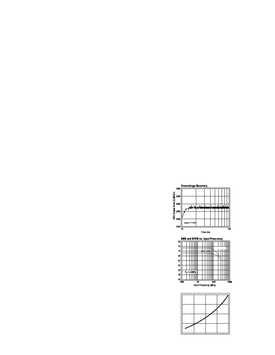
SNR & SFDR vs. Input Frequency
SNR (dB), SFDR (dBc)
Input Frequency (MHz)
80
100k
10M
100M
50
0
60
70
1M
F
S
= 20MHz
SFDR (dBc)
SNR (dB)
SNR vs. Sample Rate vs. Bias
SNR (dB)
Sample Rate (MSPS)
70
60
0.1
1.0
10
40
30
50
100
Low Bias
High Bias
Medium Bias
F
in
= 5MHz
SFDR vs. Sample Rate vs. Bias
SFDR (dBc)
Sample Rate (MSPS)
80
70
0.1
1.0
10
50
40
60
100
Low Bias
Medium Bias
High Bias
F
in
= 5MHz
Two Tone Intermodulation Distortion
Output Level (dBFS)
Frequency (MHz)
0
-40
0
2
4
-120
-80
10
6
8
-20
-60
-100
Integral Non-Linearity
INL (LSBs)
Output Code
2.5
1.5
0
1000
2000
-2.5
0.5
3000
4000
2
1
0
-0.5
-1
-1.5
-2
Differential Non-Linearity
DNL (LSBs)
Output Code
1.5
0.5
0
1000
2000
-1.5
-0.5
3000
4000
1
0
-1
Pulse Settling Response
ADC Output Code
Time (ns)
4000
0
100
150
1000
0
2000
200
3000
50
SFDR vs. Input Frequency
40
∞
C
80
∞
C
60
∞
C
0
∞
C
20
∞
C
-20
∞
C
SFDR (dBc)
Input Frequency (MHz)
80
76
72
68
64
60
1
10
100
I/O Timing (Convert CLK & Bit Skew)
p(
)
Time (ns)
400
300
0
4
16
100
0
200
20
8
12
Output Data
Convert
http://www.national.com
4
Recommended Operating Conditions
Absolute Maximum Ratings*
s
upply voltage (V
DD
)
+5V ± 5%
differential voltage between any two GND's
<10mV
analog input voltage range (full scale)
1.25 ≠ 3.25V
digital input voltage range
0 to V
DD
operating temperature range
0∞C to 70∞C
clock pulse-width high (C
pwh
)
> 25ns
supply voltage (V
DD
)
-0.5V to +7V
differential voltage between any two GND's
200mV
analog input voltage range
-0.5V to +V
DD
digital input voltage range
-0.5V to +V
DD
output short circuit duration (one pin to gnd)
infinite
junction temperature
+175∞C
storage temperature range
-65∞C to +150∞C
lead solder duration (+300∞C)
10 sec
*NOTE: Absolute maximum ratings are limiting values, to be applied individually, and beyond which the serviceability of the circuit may be impaired.
Functional operability under any of these conditions is not necessarily implied. Exposure to maximum ratings for extended periods may affect device
reliability.
Pinout & Pin Description and Usage
References (V
REFN
, V
REFP
, V
REFNO
, V
REFPO
, V
REFNC
,
V
REFPC
, V
REFMO
)
To use the internal references, connect V
REFPO
to V
REFP
and V
REFNO
to V
REFN
. The nominal value for V
REFPO
is
3.25V and for V
REFNO
is 1.25V. V
REFPC
and V
REFNC
are
internal reference points which should be bypassed to
GND with a 0.1
µ
F capacitor. V
REFMO
is an output
voltage that is equal to the mid point of the reference
range and can be used to apply the appropriate offset to
the analog inputs. For a more detailed discussion on
references, see the paragraph on references in the
applications section of this datasheet.
Analog Input (V
INP
, V
INN
)
The analog input to the CLC949 is a differential signal
applied to V
INP
and V
INN
. For more detail on driving the
inputs, see the paragraphs in the applications section of
this datasheet.
Power Supplies and Grounds (V
DDA
, V
DDD
, GND
A
, GND
D
)
The power and ground pins of the CLC949 are split into
those that supply the analog portions of the integrated
circuit (V
DDA
, GND
A
) and the digital portions of the chip
(V
DDD
, GND
D
). If your system uses separate power and
ground planes, then performance can be improved by
making use of the appropriate pins. In many systems,
the power pins will all be tied together and the GND pins
will all be tied together. For more detailed discussion,
please refer to the paragraph on power and grounds in
the applications section of the databook.
Clock (CLK)
The CLK accepts a CMOS clock input. Samples are
taken on the falling edges of the CLK and data emerges
6 1/2 clock cycles later, on to the rising edge of the CLK.
Output Data (D1-D12, MSBINV, OE\)
The data emerges from the CLC949 as CMOS level
digital data on D1(MSB) through D12(LSB). The
outputs can be put into a high impedance state by
bringing OE\ high. There is an internal pulldown
resistor so that if this input is left open, the output data is
enabled. MSBINV will invert the MSB of the output data.
With MSBINV in the high state, the output data is two's
complement, when low, the output data format is offset
binary. An internal pulldown resistor makes the output
default to offset binary if MSBINV is left open.
Bias Control (BCO, BC1, BIASC)
The DC bias current of the CLC949 is controlled by three
pins: BCO, BC1, and BIASC. BC0 and BC1 are digital
CMOS inputs and set the bias current in accordance with
the truth table below:
BC0
BC1
Bias Current
PD@10MSPS
0
0
Default: Med Bias (200
µ
A)
200mW
1
0
Analog Mode
Variable
0
1
High Bias (400
µ
A)
350mW
1
1
Low Bias (50
µ
A)
75mW
In the analog mode, the user provides a bias current
through the BIASC pin of the CLC949. As the bias
current is increased, the power dissipation of the CLC949
is increased and the part becomes capable of increased
conversion rates.
NC
No connection - leave these pins open.
44-Pin PLCC
TOP VIEW
1
2
3
4
5
6
44 43 42 41 40
V
DDD
V
DDD
V
DDD
NC
CLK
BC1
V
DDA
V
DDA
V
DDA
V
REFNO
V
REFPO
23
22
21
20
19
18
24 25 26 27 28
GND
D
GND
D
MSBINV
OE\
D1(MSB)
D2
GND
D
GND
A
GND
A
GND
A
GND
A
12
11
10
9
8
7
13
14
15
16
17
NC
BIASC
GND
A
V
INP
V
INN
GND
A
V
REFNC
V
REFPC
V
REFN
V
REFP
V
REFMO
34
35
36
37
38
39
33
32
31
30
29
D8
D7
D6
D5
D4
D3
D9
D10
D11
D12(LSB)
BCO
5
http://www.national.com
CLC949 OPERATION
Application
In a high speed data acquisition system, the overall
performance is often determined by the A/D converter
and its surrounding circuitry. You should pay special
attention to the data converter and its support circuitry if
you want to obtain the best possible performance. The
information on these pages is intended to help you
design the circuitry surrounding the CLC949 in such
a way as to achieve superior results. Additional
information is available in the form of Comlinear
applications notes. Especially useful are AD-01 and
AD-02.
Circuit Description
The CLC949 ADC consists of an input Sample-and-Hold
Amplifier (SHA) followed by a pipelined quantizer.
Internal reference sources and output data latches
complete the major functions required of an A/D
converter. Digital error correction in the quantizer helps
to provide accurate conversions of high speed dynamic
signals. The speed of the analog circuitry is determined
in part by the internal bias currents applied. The CLC949
allows you to make this important tradeoff between
power and performance through settings on two digital
control pins and for fine adjustments through the use of
an external resistor.
Timing and CLK Generation
The falling edge of the CLK pulse causes the input sam-
ple-and-hold amplifier to transition into the hold mode.
The sample is taken approximately 3ns after this falling
edge. The digitized data is presented to the output latch-
es 6 1/2 clock cycles later and is held until after the next
rising edge of CLK. This timing is shown in the timing
diagram, Figure 1.
Figure 1: Timing Diagram
The CLC949 is designed to operate with a CMOS clock
signal. To obtain the lowest possible noise when
digitizing a high frequency input, more care must be
taken in the generation of this clock than is usually
accorded to CMOS Clocks. To minimize aperture jitter
induced errors, the CLK needs to have as low a
jitter as possible and as fast an edge rate as possible. To
obtain a very low jitter clock from a sinusoidal source, the
circuit shown in Figure 2 is recommended.
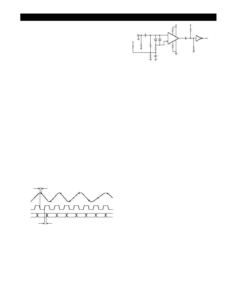
Figure 2: Clock Generation
Here the CLC006 cable driver is used as a comparator to
generate a high speed clock. The CLC006 has less than
2ps of jitter and has rise and fall times less than 1ns. The
CLC006 output is then buffered by a 74AC04 which
maintains fast edge rates and provides CMOS levels for
the CLC949. If there is excessive jitter in the CLK, then
the digitized signal will exhibit an excessive amount of
noise, especially for high frequency inputs. For a more
detailed description of this phenomenon, please read the
Comlinear Application Note AD-03.
In addition to the circuitry generating the clock, the
layout of the clock distribution network can affect the
overall performance of the converter. To obtain the best
possible performance, a clock driver with very low output
impedance and fast edge rates such as the 74AC04,
should be placed as close as possible to the CLC949
clock input pin. Additional length in the circuit trace for
the clock will cause an increase in the jitter seen by the
converter.
On the CLC949 evaluation board, the
E949PCASM, there is less than 1/16th of an inch
between the 74AC04 that is driving the clock input and
the input to the CLC949. If the system has several
CLC949s, and jitter is liable to generate problems, then
use a separate clock driver for each CLC949. Each
driver should be placed as close to the converter that it is
driving as is practicable.
Driving the Differential Input
The CLC949 has a differential input with a common
mode voltage of 2.25V. Since not all applications have a
signal preconditioned in this manner there is often a need
to do a single-ended-to-differential conversion and to add
offset. In systems which do not need to be DC coupled,
the best method for doing this is with an RF transformer
such as the Minicircuits TMO1-1T. This is an RF
transformer with a center tapped secondary which will
operate over a frequency range of 50kHz to 200MHz.
You can offset the input and split the phases simply by
connecting the center tap to the mid scale reference
output (V
REFMO
) as shown in Figure 3.
This set up can be realized on the CLC949 evaluation
board by enabling option 1. See E949PCASM data
sheet for details. A transformer coupled input will allow
the CLC949 to exhibit the best possible distortion
performance for high frequency input signals.
Analog
Input
CLK
Output
Data
Effective Aperture Delay
Output Hold Time
Sample 0
Sample 1
Sample 2
Sample
3
Sample 4
Sample
5
Sample 6
Sample 7
Sample
-3 Valid
Sample
-2 Valid
Sample
-1 Valid
Sample
0 Valid
Sinusoisal
Clock Input
50
9
3
1
4
6
+5V
+
-
50
CLC006
1k
0.1
µ
F
10k
0.1
µ
F
2.2k
2.2k
8
5
10k
10k
+5V
0.1
µ
F
74AC04
To CLC949
Clock
1k
+5V