 | –≠–ª–µ–∫—Ç—Ä–æ–Ω–Ω—ã–π –∫–æ–º–ø–æ–Ω–µ–Ω—Ç: COP225C | –°–∫–∞—á–∞—Ç—å:  PDF PDF  ZIP ZIP |
TL DD 8422
COP224CCOP225CCOP226CCOP244CCOP245C
Single-Chip
1k
and
2k
CMOS
Microcontrollers
May 1992
COP224C COP225C COP226C COP244C COP245C
Single-Chip 1k and 2k CMOS Microcontrollers
General Description
The COP224C
COP225C
COP226C
COP244C and
COP245C fully static Single-Chip CMOS Microcontrollers
are members of the COPS
TM
family fabricated using dou-
ble-poly silicon gate microCMOS technology These Con-
troller Oriented Processors are complete microcomputers
containing all system timing internal logic ROM RAM and
I O necessary to implement dedicated control functions in a
variety of applications Features include single supply oper-
ation a variety of output configuration options with an in-
struction set internal architecture and I O scheme de-
signed to facilitate keyboard input display output and BCD
data manipulation The COP224C and COP244C are 28 pin
chips The COP225C and COP245C are 24-pin versions (4
inputs removed) and COP226C is 20-pin version with 15 I O
lines Standard test procedures and reliable high-density
techniques provide the medium to large volume customers
with a customized microcontroller at a low end-product cost
These microcontrollers are appropriate choices in many de-
manding control environments especially those with human
interface
COPS
TM
Microbus
TM
and MICROWIRE
TM
are trademarks of National Semiconductor Corp
TRI-STATE
is a registered trademark of National Semiconductor Corp
Features
Y
Lowest power dissipation (600 mW typical)
Y
Fully static (can turn off the clock)
Y
Power saving IDLE state and HALT mode
Y
4 4 ms instruction time
Y
2k x 8 ROM 128 x 4 RAM (COP244C COP245C)
Y
1k x 8 ROM
64 x 4 RAM (COP224C COP225C
COP226C)
Y
23 I O lines (COP244C and COP224C)
Y
True vectored interrupt plus restart
Y
Three-level subroutine stack
Y
Single supply operation (4 5V to 5 5V)
Y
Programmable read write 8-bit timer event counter
Y
Internal binary counter register with MICROWIRE
TM
serial I O capability
Y
General purpose and TRI-STATE
outputs
Y
LSTTL CMOS output compatible
Y
Software hardware compatible with COP400 family
Y
Military temperature (
b
55 C to
a
125 C) operation
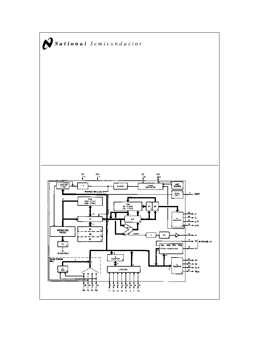
Block Diagram
Not available on COP226C
TL DD 8422 ≠ 1
FIGURE 1
C1995 National Semiconductor Corporation
RRD-B30M105 Printed in U S A
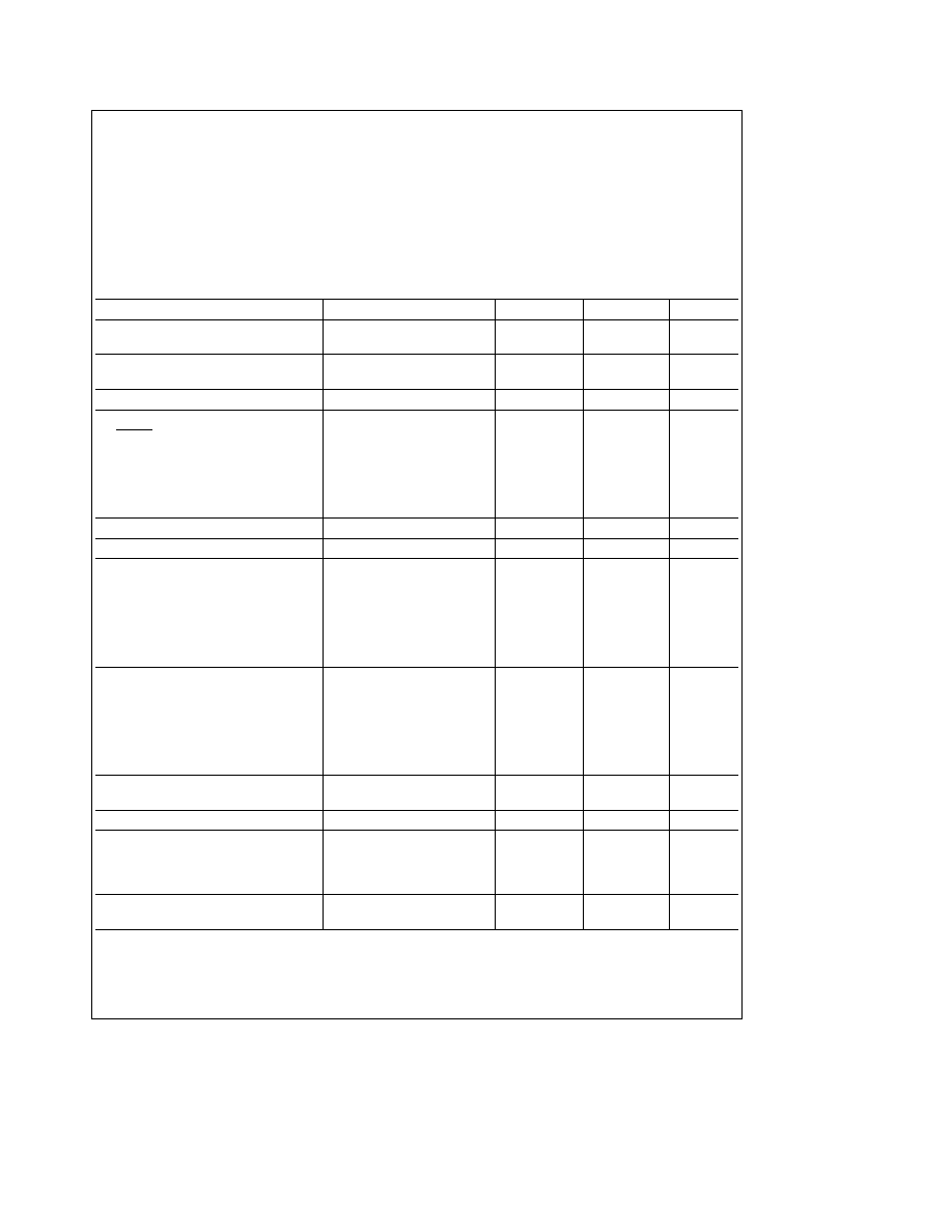
Absolute Maximum Ratings
If Military Aerospace specified devices are required
please contact the National Semiconductor Sales
Office Distributors for availability and specifications
Supply Voltage (V
CC
)
6V
Voltage at any Pin
b
0 3V to V
CC
a
0 3V
Total Allowable Source Current
25 mA
Total Allowable Sink Current
25 mA
Total Allowable Power Dissipation
150 mW
Operating Temperature Range
b
55 C to
a
125 C
Storage Temperature Range
b
65 C to
a
150 C
Lead Temperature
(soldering 10 seconds)
300 C
Note
Absolute maximum ratings indicate limits beyond
which damage to the device may occur DC and AC electri-
cal specifications are not ensured when operating the de-
vice at absolute maximum ratings
DC Electrical Characteristics
b
55 C
s
T
A
s
a
125 C
a
4 5V
s
V
CC
s
a
5 5V unless otherwise specified
Parameter
Conditions
Min
Max
Units
Operating Voltage
4 5
5 5
V
Power Supply Ripple (Notes 4 5)
Peak to Peak
0 25 V
CC
V
Supply Current
V
CC
e
5 0V tc
e
4 4 ms
5
mA
(Note 1)
(tc is instruction cycle time)
HALT Mode Current (Note 2)
V
CC
e
5 0V F
IN
e
0 kHz
200
m
A
Input Voltage Levels
RESET CKI D
0
(clock input)
Logic High
0 9 V
CC
V
Logic Low
0 1 V
CC
V
All Other Inputs
Logic High
0 7 V
CC
V
Logic Low
0 2 V
CC
V
Hi-Z Input Leakage
b
10
a
10
m
A
Input Capacitance (Note 4)
7
pF
Output Voltage Levels (except CKO)
Standard Outputs
LSTTL Operation
V
CC
e
5 0V
g
10%
Logic High
I
OH
e b
100 mA
2 7
V
Logic Low
I
OL
e
400 mA
0 6
V
CMOS Operation
Logic High
I
OH
e b
10 mA
V
CC
b
0 2
V
Logic Low
I
OL
e
10 mA
0 2
V
CKO Current Levels (As Clock Out)
Sink
d
4
0 2
mA
d
8
CKI
e
V
CC
V
OUT
e
V
CC
0 4
mA
d
16
(
0 8
mA
Source
d
4
b
0 2
mA
d
8
CKI
e
0V V
OUT
e
0V
b
0 4
mA
d
16
(
b
0 8
mA
Allowable Sink Source Current per Pin
5
mA
(Note 6)
Allowable Loading on CKO (as HALT)
50
pF
Current Needed to Over-Ride HALT
(Note 3)
To Continue
V
IN
e
0 2 V
CC
2 0
mA
To Halt
V
IN
e
0 7 V
CC
3 0
mA
TRI-STATE or Open Drain
Leakage Current
b
10
a
10
m
A
2
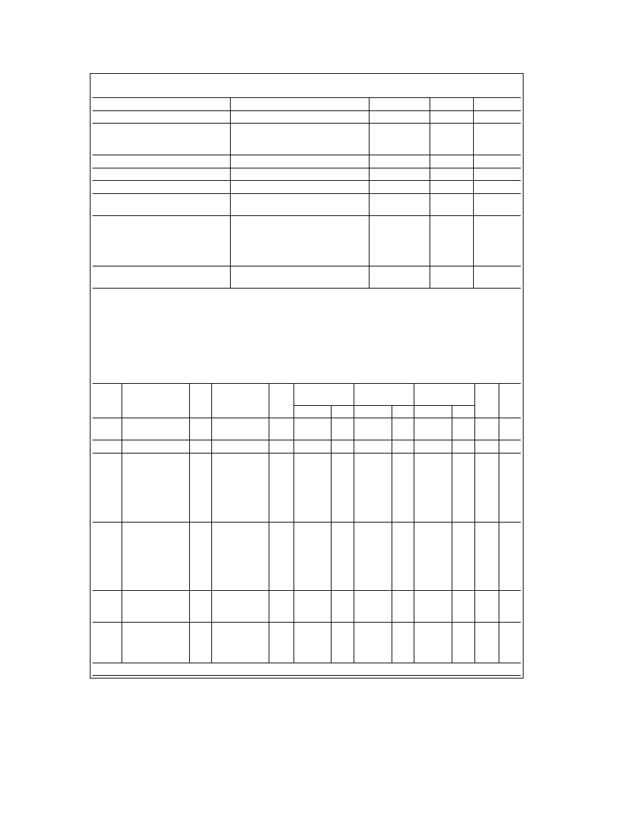
AC Electrical Characteristics
b
55 C
s
T
A
s
a
125 C
a
4 5V
s
V
CC
s
a
5 5V unless otherwise specified
Parameter
Conditions
Min
Max
Units
Instruction Cycle Time (tc)
4 4
DC
m
s
Operating CKI
d
4 mode
DC
0 9
MHz
Frequency
d
8 mode
DC
1 8
MHz
d
16 mode
(
DC
3 6
MHz
Duty Cycle (Note 4)
f
1
e
3 6 MHz
40
60
%
Rise Time (Note 4)
f
1
e
3 6 MHz External Clock
60
ns
Fall Time (Note 4)
f
1
e
3 6 MHz External Clock
40
ns
Instruction Cycle Time
R
e
30k
g
5%
RC Oscillator (Note 4)
C
e
82 pF
g
5% (
d
4 Mode)
6
18
m
s
Inputs (See
Figure 3 ) (Note 4)
t
SETUP
G Inputs
tc 4
a
0 8
m
s
SI Input
0 33
m
s
All Others
1 9
m
s
t
HOLD
0 4
m
s
Output Propagation Delay
V
OUT
e
1 5V C
L
e
100 pF R
L
e
5k
t
PD1
t
PD0
1 4
m
s
Note 1
Supply current is measured after running for 2000 cycle times with a square-wave clock on CKI CKO open and all other pins pulled up to V
CC
with 5k
resistors See current drain equation on page 13
Note 2
The HALT mode will stop CKI from oscillating in the RC and crystal configurations Test conditions all inputs tied to V
CC
L lines in TRI-STATE mode and
tied to ground all outputs low and tied to ground
Note 3
When forcing HALT current is only needed for a short time (approx 200 ns) to flip the HALT flip-flop
Note 4
This parameter is not tested but guaranteed by design Variation due to the device included
Note 5
Voltage change must be less than 0 25 volts in a 1 ms period
Note 6
SO output sink current must be limited to keep V
OL
less than 0 2 V
CC
when part is running in order to prevent entering test mode
RETS COP244CX DC Parameters
Test Conditions 5 3V
s
V
CC
s
3V Unless Otherwise Specified
Symbol
Parameter
(Note 1)
V
CC
Conditions
Test
SBGRP 1
SBGRP 2
SBGRP 3
Limits
(25 C)
Drift
Units
a
25 C
a
125 C
b
55 C
Min
Max
Min
Max
Min
Max
I
DD1
Supply Current
V
DD
e
4V
85
155
85
m
A
F
IN
e
64 kHz
I
DD2
Halt Current
V
DD
e
4V
35
125
35
m
A
Input Voltage
Reset CKI
V
IH1
Logic High
9 V
CC
9 V
CC
9 V
CC
V
V
IL1
Logic Low
1 V
CC
1 V
CC
1 V
CC
V
All Other Inputs
V
IH2
Logic High
7 V
CC
7 V
CC
7 V
CC
V
V
IL2
Logic Low
2 V
CC
2 V
CC
2 V
CC
V
Output Voltage
LSTTL Operation
V
OH1
Logic High
4 75V I
OH
e b
100 mA
2 7
2 7
2 7
V
V
OL1
Logic Low
4 75V I
OL
e
400 mA
0 4
0 4
0 4
V
CMOS Operation
V
OH2
Logic High
4 75V I
OH
e b
10 mA
V
CC
b
0 2
V
CC
b
0 2
V
CC
b
0 2
V
V
OL2
Logic Low
4 75V I
OL
e
10 mA
0 2
0 2
0 2
V
Output Current
I
OH
Logic High
3V
V
e
0V
b
100
b
100
b
100
m
A
I
OL
Logic Low
3V
V
e
3V
200
200
200
m
A
Input Leakage
I
IN1
High-Z
b
2 5
2 5
b
2 5
2 5
b
2 5
2 5
m
A
I
IN2
TRI-STATE or
b
4
4
b
4
4
b
4
4
m
A
Open Drain
RETS COP244CX
DEVICE COP244C-XXX 883
FUNCTION 4-BIT CMOS MICROCONTROLLER
3
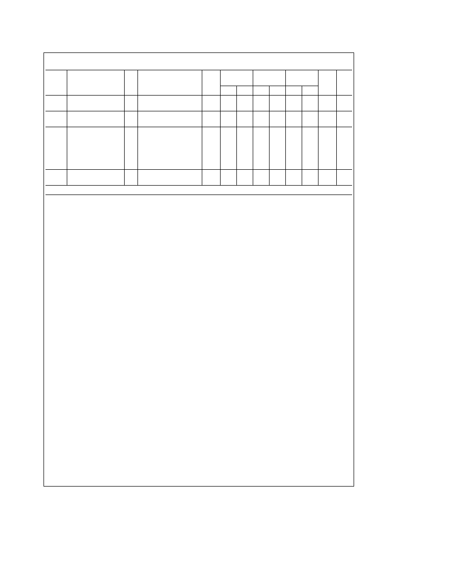
RETS COP244CX AC Parameters
Test Conditions 5 3V
s
V
CC
s
3V Unless Otherwise Specified
Symbol
Parameter
V
CC
Conditions
Test
SBGRP 9
SBGRP 10
SBGRP 11
Limits
(25 C)
Drift
Units
a
25 C
a
125 C
b
55 C
Min
Max
Min
Max
Min
Max
t
CC
Instruction Cycle
Mode Divided by 8
80
125
80
125
80
125
m
s
Time (Note 1)
V
DD
e
3V
F
IN
Operating Clock
V
DD
e
3V
64
100
64
100
64
100
kHz
Frequency (Note 1)
30%
s
Duty Cycle
s
50%
Inputs
t
SETUP
(Note 2)
V
e
4 5V
2
2
2
m
s
t
SETUP-G
Inputs
32
32
32
m
s
For SKGZ
SKGBZ
(Note 2)
t
HOLD
(Note 1)
0 6
0 6
0 6
m
s
t
PD1
Output Prop Delay
4 5V
R
L
e
5k C
L
e
100 pF
6
6
6
m
s
t
PD2
(Note 1)
V
OUT
e
1 5V
6
6
6
m
s
RETS COP244CX
DEVICE COP244C-XXXD 883
FUNCTION 4-BIT CMOS MICROCONTROLLER
Note 1
Parameter tested go-no-go only
Note 2
Guaranteed by design and not tested
4
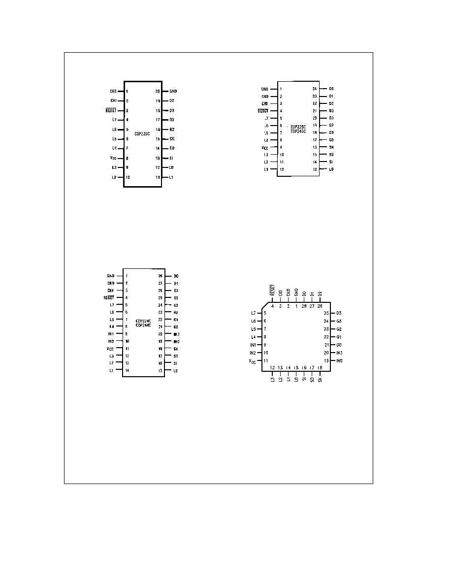
Connection Diagrams
S O Wide and DIP
Top View
TL DD 8422 ≠ 2
Order Number COP226C-XXX N
See NS Molded Package Number N20A
Order Number COP226C-XXX D
See NS Hermetic Package Number D20A
Order Number COP226C-XXX WM
See NS Surface Mount Package Number M20B
S O Wide and DIP
Top View
TL DD 8422 ≠ 3
Order Number COP225C-XXX N
or COP245C-XXX N
See NS Molded Package Number N24A
Order Number COP225C-XXX D
or COP245C-XXX D
See NS Hermetic Package Number D24C
DIP
Top View
TL DD 8422 ≠ 4
Order Number COP224C-XXX N
or COP244C-XXX N
See NS Molded Package Number N28B
Order Number COP224C-XXX D
or COP244C-XXX D
See NS Hermetic Package Number D28C
28 PLCC
TL DD 8422 ≠ 13
Order Number COP224C-XXX V
or COP244C-XXX V
See NS PLCC Package Number V28A
FIGURE 2
5