 | –≠–ª–µ–∫—Ç—Ä–æ–Ω–Ω—ã–π –∫–æ–º–ø–æ–Ω–µ–Ω—Ç: COP310L | –°–∫–∞—á–∞—Ç—å:  PDF PDF  ZIP ZIP |
TL DD 6919
COP410LCOP411LCOP310LCOP311L
Single-Chip
N-Channel
Microcontrollers
March 1992
COP410L COP411L COP310L COP311L
Single-Chip N-Channel Microcontrollers
General Description
The COP410L and COP411L Single-Chip N-Channel Micro-
controllers are members of the COPS
TM
family fabricated
using N-channel silicon gate MOS technology These Con-
troller Oriented Processors are complete microcomputers
containing all system timing internal logic ROM RAM and
I O necessary to implement dedicated control functions in a
variety of applications Features include single supply oper-
ation a variety of output configuration options with an in-
struction set internal architecture and I O scheme de-
signed to facilitate keyboard input display output and BCD
data manipulation
The COP411L is identical to the
COP410L but with 16 I O lines instead of 19 They are an
appropriate choice for use in numerous human interface
control environments Standard test procedures and reliable
high-density fabrication techniques provide the medium to
large volume customers with a customized Controller Ori-
ented Processor at a low end-product cost
The COP310L and COP311L are exact functional equiva-
lents but extended temperature versions of COP410L and
COP411L respectively
The COP401L should be used for exact emulation
Features
Y
Low cost
Y
Powerful instruction set
Y
512 x 8 ROM 32 x 4 RAM
Y
19 I O lines (COP410L)
Y
Two-level subroutine stack
Y
16 ms instruction time
Y
Single supply operation (4 5V ≠ 6 3V)
Y
Low current drain (6 mA max)
Y
Internal binary counter register with MICROWIRE
TM
se-
rial I O capability
Y
General purpose and TRI-STATE
outputs
Y
LSTTL CMOS compatible in and out
Y
Direct drive of LED digit and segment lines
Y
Software hardware compatible with other members of
COP400 family
Y
Extended temperature range device
COP310L COP311L (
b
40 C to
a
85 C)
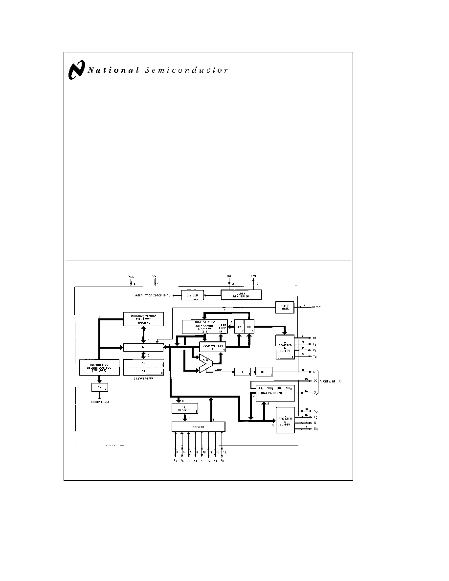
Block Diagram
TL DD 6919 ≠ 1
FIGURE 1 COP410L
COPS
TM
and MICROWIRE
TM
are trademarks of National Semiconductor Corporation
TRI-STATE
is a registered trademark of National Semiconductor Corporation
C1995 National Semiconductor Corporation
RRD-B30M105 Printed in U S A

COP410L COP411L
Absolute Maximum Ratings
If Military Aerospace specified devices are required
please contact the National Semiconductor Sales
Office Distributors for availability and specifications
Voltage at Any Pin Relative to GND
b
0 5V to
a
10V
Ambient Operating Temperature
0 C to
a
70 C
Ambient Storage Temperature
b
65 C to
a
150 C
Lead Temperature
(Soldering 10 seconds)
300 C
Power Dissipation
COP410L
0 75W at 25 C
0 4W at 70 C
COP411L
0 65W at 25 C
0 3W at 70 C
Total Source Current
120 mA
Total Sink Current
100 mA
Note
Absolute maximum ratings indicate limits beyond
which damage to the device may occur DC and AC electri-
cal specifications are not ensured when operating the de-
vice at absolute maximum ratings
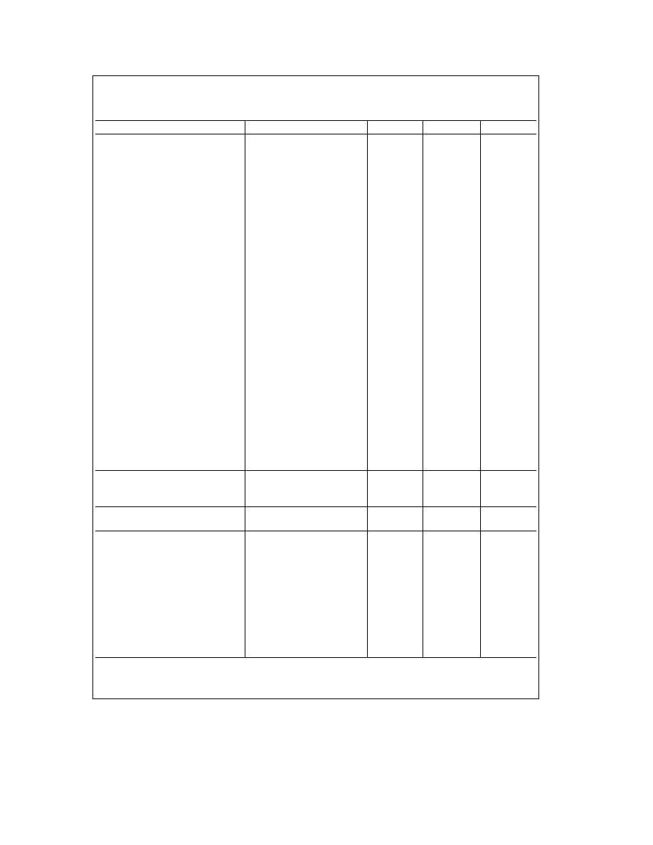
DC Electrical Characteristics
0 C
s
T
A
s
a
70 C 4 5V
s
V
CC
s
6 3V unless otherwise noted
Parameter
Conditions
Min
Max
Units
Standard Operating Voltage (V
CC
)
4 5
6 3
V
Power Supply Ripple (Notes 1 4)
Peak to Peak
0 5
V
Operating Supply Current
All Inputs and Outputs Open
6
mA
Input Voltage Levels
CKI Input Levels
Ceramic Resonator Input (
d
8)
Logic High (V
IH
)
V
CC
e
Max
3 0
V
Logic High (V
IH
)
V
CC
e
5V
g
5%
2 0
V
Logic Low (V
IL
)
b
0 3
0 4
V
Schmitt Trigger Input (
d
4)
Logic High (V
IH
)
0 7 V
CC
V
Logic Low (V
IL
)
b
0 3
0 6
V
RESET Input Levels
(Schmitt Trigger Input)
Logic High
0 7 V
CC
V
Logic Low
b
0 3
0 6
V
SO Input Level (Test Mode)
(Note 2)
2 0
2 5
V
All Other Inputs
Logic High
V
CC
e
Max
3 0
V
Logic High
With TTL Trip Level Options
2 0
V
Logic Low
Selected V
CC
e
5V
g
5%
b
0 3
0 8
V
Logic High
With High Trip Level Options
3 6
V
Logic Low
Selected
b
0 3
1 2
V
Input Capacitance (Note 4)
7
pF
Hi-Z Input Leakage
b
1
a
1
m
A
Output Voltage Levels
LSTTL Operation
V
CC
e
5V
g
10%
Logic High (V
OH
)
I
OH
e b
25 mA
2 7
V
Logic Low (V
OL
)
I
OL
e
0 36 mA
0 4
V
CMOS Operation (Note 3)
Logic High
I
OH
e b
10 mA
V
CC
b
1
V
Logic Low
I
OL
e a
10 mA
0 2
V
Note 1
V
CC
voltage change must be less than 0 5V in a 1 ms period to maintain proper operation
Note 2
SO output ``0'' level must be less than 0 8V for normal operation
Note 3
TRI-STATE
and LED configurations are excluded
Note 4
This parameter is only sampled and not 100% tested Variation due to the device included
2
COP410L COP411L
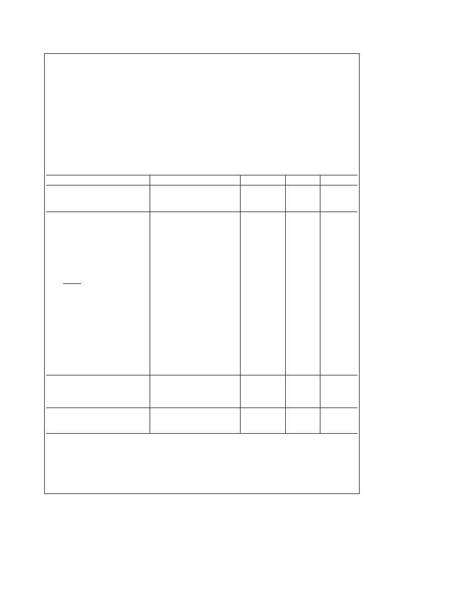
DC Electrical Characteristics
0 C
s
T
A
s
a
70 C 4 5V
s
V
CC
s
6 3V unless otherwise noted (Continued)
Parameter
Conditions
Min
Max
Units
Output Current Levels
Output Sink Current
SO and SK Outputs (I
OL
)
V
CC
e
6 3V V
OL
e
0 4V
1 2
mA
V
CC
e
4 5V V
OL
e
0 4V
0 9
mA
L
0
≠ L
7
Outputs G
0
≠ G
3
and
V
CC
e
6 3V V
OL
e
0 4V
0 4
mA
LSTTL D
0
≠ D
3
Outputs (I
OL
)
V
CC
e
4 5V V
OL
e
0 4V
0 4
mA
D
0
≠ D
3
Outputs with High
V
CC
e
6 3V V
OL
e
1 0V
11
mA
Current Options (I
OL
)
V
CC
e
4 5V V
OL
e
1 0V
7 5
mA
D
0
≠ D
3
Outputs with Very
V
CC
e
6 3V V
OL
e
1 0V
22
mA
High Current Options (I
OL
)
V
CC
e
4 5V V
OL
e
1 0V
15
mA
CKI (Single-Pin RC Oscillator)
V
CC
e
4 5V V
IH
e
3 5V
2
mA
CKO
V
CC
e
4 5V V
OL
e
0 4V
0 2
mA
Output Source Current
Standard Configuration
V
CC
e
6 3V V
OH
e
2 0V
b
75
b
480
m
A
All Outputs (I
OH
)
V
CC
e
4 5V V
OH
e
2 0V
b
30
b
250
m
A
Push-Pull Configuration
V
CC
e
6 3V V
OH
e
2 4V
b
1 4
mA
SO and SK Outputs (I
OH
)
V
CC
e
4 5V V
OH
e
1 0V
b
1 2
mA
LED Configuration L
0
≠ L
7
V
CC
e
6 0V V
OH
e
2 0V
b
1 5
b
13
mA
Outputs Low Current
Driver Option (I
OH
)
LED Configuration L
0
≠ L
7
V
CC
e
6 0V V
OH
e
2 0V
b
3 0
b
25
mA
Outputs High Current
Driver Option (I
OH
)
TRI-STATE Configuration
V
CC
e
6 3V V
OH
e
3 2V
b
0 8
mA
L
0
≠ L
7
Outputs Low
V
CC
e
4 5V V
OH
e
1 5V
b
0 9
mA
Current Driver Option (I
OH
)
TRI-STATE Configuration
V
CC
e
6 3V V
OH
e
3 2V
b
1 6
mA
L
0
≠ L
7
Outputs High
V
CC
e
4 5V V
OH
e
1 5V
b
1 8
mA
Current Driver Option (I
OH
)
Input Load Source Current
V
CC
e
5 0V V
IL
e
0V
b
10
b
140
m
A
CKO Output
RAM Power Supply Option
V
R
e
3 3V
1 5
mA
Power Requirement
TRI-STATE Output Leakage
b
2 5
a
2 5
m
A
Current
Total Sink Current Allowed
All Outputs Combined
100
mA
D Port
100
mA
L
7
≠ L
4
G Port
4
mA
L
3
≠ L
0
4
mA
Any Other Pin
2 0
mA
Total Source Current Allowed
All I O Combined
120
mA
L
7
≠ L
4
60
mA
L
3
≠ L
0
60
mA
Each L Pin
25
mA
Any Other Pin
1 5
mA
3
COP310L COP311L
Absolute Maximum Ratings
If Military Aerospace specified devices are required
please contact the National Semiconductor Sales
Office Distributors for availability and specifications
Voltage at Any Pin Relative to GND
b
0 5V to
a
10V
Ambient Operating Temperature
b
40 C to
a
85 C
Ambient Storage Temperature
b
65 C to
a
150 C
Lead Temperature
(Soldering 10 seconds)
300 C
Power Dissipation
COP310L
0 75W at 25 C
0 25W at 85 C
COP311L
0 65W at 25 C
0 20W at 85 C
Total Source Current
120 mA
Total Sink Current
100 mA
Note
Absolute maximum ratings indicate limits beyond
which damage to the device may occur DC and AC electri-
cal specifications are not ensured when operating the de-
vice at absolute maximum ratings
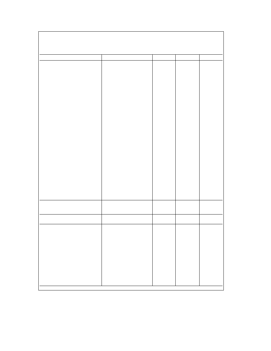
DC Electrical Characteristics
b
40 C
s
T
A
s
a
85 C 4 5V
s
V
CC
s
5 5V unless otherwise noted
Parameter
Conditions
Min
Max
Units
Standard Operating Voltage (V
CC
)
4 5
5 5
V
Power Supply Ripple (Notes 1 4)
Peak to Peak
0 5
V
Operating Supply Current
All Inputs and Outputs Open
8
mA
Input Voltage Levels
Ceramic Resonator Input (
d
8)
Crystal Input
Logic High (V
IH
)
V
CC
e
Max
3 0
V
Logic High (V
IH
)
V
CC
e
5V
g
5%
2 2
V
Logic Low (V
IL
)
b
0 3
0 3
V
Schmitt Trigger Input (
d
4)
Logic High (V
IH
)
0 7 V
CC
V
Logic Low (V
IL
)
b
0 3
0 4
V
RESET Input Levels
(Schmitt Trigger Input)
Logic High
0 7 V
CC
V
Logic Low
b
0 3
0 4
V
SO Input Level (Test Mode)
(Note 2)
2 2
2 5
V
All Other Inputs
Logic High
V
CC
e
Max
3 0
V
Logic High
With TTL Trip Level Options
2 2
V
Logic Low
Selected V
CC
e
5V
g
5%
b
0 3
0 6
V
Logic High
With High Trip Level Options
3 6
V
Logic Low
Selected
b
0 3
1 2
V
Input Capacitance (Note 4)
7
pF
Hi-Z Input Leakage
b
2
a
2
m
A
Output Voltage Levels
LSTTL Operation
V
CC
e
5V
g
10%
Logic High (V
OH
)
I
OH
e b
20 mA
2 7
V
Logic Low (V
OL
)
I
OL
e
0 36 mA
0 4
V
CMOS Operation (Note 3)
Logic High
I
OH
e b
10 mA
V
CC
b
1
V
Logic Low
I
OL
e a
10 mA
0 2
V
Note 1
V
CC
voltage change must be less than 0 5V in a 1 ms period to maintain proper operation
Note 2
SO output ``0'' level must be less than 0 6V for normal operation
Note 3
TRI-STATE and LED configurations are excluded
Note 4
This parameter is only sampled and not 100% tested Variation due to the device included
4
COP310L COP311L
DC Electrical Characteristics
(Continued)
b
40 C
s
T
A
s
a
85 C 4 5V
s
V
CC
s
5 5V unless othewise noted
Parameter
Conditions
Min
Max
Units
Output Current Levels
Output Sink Current
SO and SK Outputs (I
OL
)
V
CC
e
5 5V V
OL
e
0 4V
1 0
mA
V
CC
e
4 5V V
OL
e
0 4V
0 8
mA
L
0
≠ L
7
Outputs G
0
≠ G
3
and
V
CC
e
5 5V V
OL
e
0 4V
0 4
mA
LSTTL D
0
≠ D
3
Outputs (I
OL
)
V
CC
e
4 5V V
OL
e
0 4V
0 4
mA
D
0
≠ D
3
Outputs with High
V
CC
e
5 5V V
OL
e
1 0V
9
mA
Current Options (I
OL
)
V
CC
e
4 5V V
OL
e
1 0V
7
mA
D
0
≠ D
3
Outputs with Very
V
CC
e
5 5V V
OL
e
1 0V
18
mA
High Current Options (I
OL
)
V
CC
e
4 5V V
OL
e
1 0V
14
mA
CKI (Single-Pin RC Oscillator)
V
CC
e
4 5V V
IH
e
3 5V
1 5
mA
CKO
V
CC
e
4 5V V
OL
e
0 4V
0 2
mA
Output Source Current
Standard Configuration
V
CC
e
5 5V V
OH
e
2 0V
b
55
b
600
m
A
All Outputs (I
OH
)
V
CC
e
4 5V V
OH
e
2 0V
b
28
b
350
m
A
Push-Pull Configuration
V
CC
e
5 5V V
OH
e
2 0V
b
1 1
mA
SO and SK Outputs (I
OH
)
V
CC
e
4 5V V
OH
e
1 0V
b
1 2
mA
LED Configuration L
0
≠ L
7
V
CC
e
5 5V V
OH
e
2 0V
b
0 7
b
15
m
A
Outputs Low Current
Driver Option (I
OH
)
LED Configuration L
0
≠ L
7
V
CC
e
5 5V V
OH
e
2 0V
b
1 4
b
30
m
A
Outputs High Current
Driver Option (I
OH
)
TRI-STATE Configuration
V
CC
e
5 5V V
OH
e
2 7V
b
0 6
mA
L
0
≠ L
7
Outputs Low
V
CC
e
4 5V V
OH
e
1 5V
b
0 9
mA
Current Driver Option (I
OH
)
TRI-STATE Configuration
V
CC
e
5 5V V
OH
e
2 7V
b
1 2
mA
L
0
≠ L
7
Outputs High
V
CC
e
4 5V V
OH
e
1 5V
b
1 8
mA
Current Driver Option (I
OH
)
Input Load Source Current
V
CC
e
5 0V V
IL
e
0V
b
10
b
200
m
A
CKO Output
RAM Power Supply Option
V
R
e
3 3V
2 0
mA
Power Requirement
TRI-STATE Output Leakage
b
5
a
5
m
A
Current
Total Sink Current Allowed
All Outputs Combined
100
mA
D Port
100
mA
L
7
≠ L
4
G Port
4
mA
L
3
≠ L
0
4
mA
Any Other Pins
1 5
mA
Total Source Current Allowed
All I O Combined
120
mA
L
7
≠ L
4
60
mA
L
3
≠ L
0
60
mA
Each L Pin
25
mA
Any Other Pins
1 5
mA
5