TL DD 5259
COP424C
COP425C
COP426C
COP324C
COP325C
COP326C
and
COP444C
COP445C
COP344C
COP345C
Single-Chip
1k
and
2k
CMOS
Microcontrollers
April 1992
COP424C COP425C COP426C COP324C COP325C
COP326C and COP444C COP445C COP344C COP345C
Single-Chip 1k and 2k CMOS Microcontrollers
General Description
The COP424C
COP425C
COP426C
COP444C and
COP445C fully static Single-Chip CMOS Microcontrollers
are members of the COPS
TM
family fabricated using dou-
ble-poly silicon gate microCMOS technology These Con-
troller Oriented Processors are complete microcomputers
containing all system timing internal logic ROM RAM and
I O necessary to implement dedicated control functions in a
variety of applications Features include single supply oper-
ation a variety of output configuration options with an in-
struction set internal architecture and I O scheme de-
signed to facilitate keyboard input display output and BCD
data manipulation The COP424C and COP444C are 28 pin
chips The COP425C and COP445C are 24-pin versions (4
inputs removed) and COP426C is 20-pin version with 15 I O
lines Standard test procedures and reliable high-density
techniques provide the medium to large volume customers
with a customized microcontroller at a low end-product cost
These microcontrollers are appropriate choices in many de-
manding control environments especially those with human
interface
The COP424C is an improved product which replaces the
COP420C
COPS
TM
Microbus
TM
and MICROWIRE
TM
are trademarks of National Semiconductor Corp
TRI-STATE
is a registered trademark of National Semiconductor Corp
Features
Y
Lowest power dissipation (50 mW typical)
Y
Fully static (can turn off the clock)
Y
Power saving IDLE state and HALT mode
Y
4 ms instruction time plus software selectable clocks
Y
2k x 8 ROM 128 x 4 RAM (COP444C COP445C)
Y
1k x 8 ROM
64 x 4 RAM (COP424C COP425C
COP426C)
Y
23 I O lines (COP444C and COP424C)
Y
True vectored interrupt plus restart
Y
Three-level subroutine stack
Y
Single supply operation (2 4V to 5 5V)
Y
Programmable read write 8-bit timer event counter
Y
Internal binary counter register with MICROWIRE
TM
serial I O capability
Y
General purpose and TRI-STATE
outputs
Y
LSTTL CMOS output compatible
Y
Microbus
TM
compatible
Y
Software hardware compatible with COP400 family
Y
Extended temperature range devices COP324C
COP325C COP326C and COP344C COP345C (
b
40 C
to
a
85 C)
Y
Military devices (
b
55 C to
a
125 C) to be available
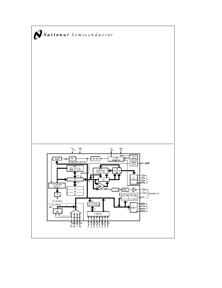
Block Diagram
Not available on COP426C COP326C
TL DD 5259 � 1
FIGURE 1
C1995 National Semiconductor Corporation
RRD-B30M105 Printed in U S A
COP424C COP425C COP426C and COP444C COP445C
Absolute Maximum Ratings
Supply Voltage (V
CC
)
6V
Voltage at any Pin
b
0 3V to V
CC
a
0 3V
Total Allowable Source Current
25 mA
Total Allowable Sink Current
25 mA
Operating Temperature Range
0 C to
a
70 C
Storage Temperature Range
b
65 C to
a
150 C
Lead Temperature
(soldering 10 seconds)
300 C
Note
Absolute maximum ratings indicate limits beyond
which damage to the device may occur DC and AC electri-
cal specifications are not ensured when operating the de-
vice at absolute maximum ratings
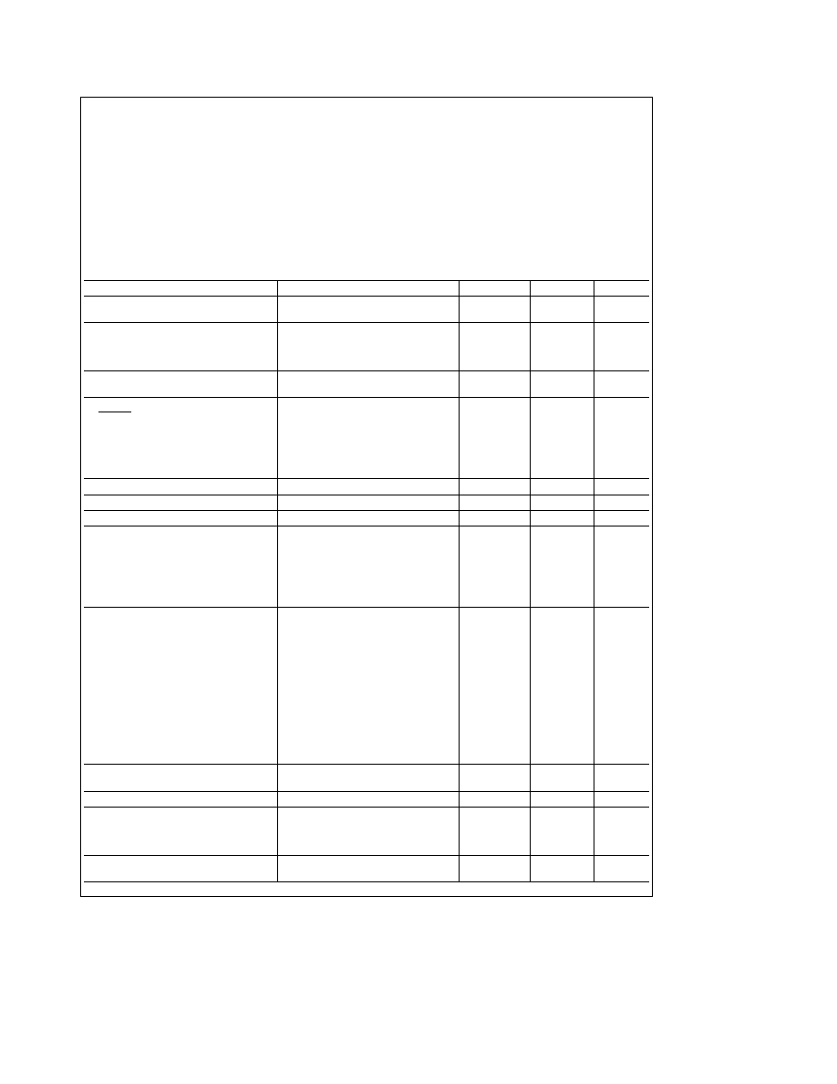
DC Electrical Characteristics
0 C
s
T
A
s
70 C unless otherwise specified
Parameter
Conditions
Min
Max
Units
Operating Voltage
2 4
5 5
V
Power Supply Ripple (Notes 4 5)
Peak to Peak
0 1 V
CC
V
Supply Current
V
CC
e
2 4V tc
e
64 ms
120
m
A
(Note 1)
V
CC
e
5 0V tc
e
16 ms
700
m
A
V
CC
e
5 0V tc
e
4 ms
3000
m
A
(tc is instruction cycle time)
HALT Mode Current
V
CC
e
5 0V F
IN
e
0 kHz
40
m
A
(Note 2)
V
CC
e
2 4V F
IN
e
0 kHz
12
m
A
Input Voltage Levels
RESET CKI D
0
(clock input)
Logic High
0 9 V
CC
V
Logic Low
0 1 V
CC
V
All Other Inputs
Logic High
0 7 V
CC
V
Logic Low
0 2 V
CC
V
Input Pull-Up Current
V
CC
e
4 5V V
IN
e
0
b
30
b
330
m
A
Hi-Z Input Leakage
b
1
a
1
m
A
Input Capacitance (Note 4)
7
pF
Output Voltage Levels
Standard Outputs
LSTTL Operation
V
CC
e
5 0V
g
10%
Logic High
I
OH
e b
100 mA
2 7
V
Logic Low
I
OL
e
400 mA
0 4
V
CMOS Operation
Logic High
I
OH
e b
10 mA
V
CC
b
0 2
V
Logic Low
I
OL
e
10 mA
0 2
V
Output Current Levels (except CKO)
Sink (Note 6)
V
CC
e
4 5V V
OUT
e
V
CC
1 2
mA
V
CC
e
2 4V V
OUT
e
V
CC
0 2
mA
Source (Standard Option)
V
CC
e
4 5V V
OUT
e
0V
b
0 5
mA
V
CC
e
2 4V V
OUT
e
0V
b
0 1
mA
Source (Low Current Option)
V
CC
e
4 5V V
OUT
e
0V
b
30
b
330
m
A
V
CC
e
2 4V V
OUT
e
0V
b
6
b
80
m
A
CKO Current Levels (As Clock Out)
Sink
d
4
0 3
mA
d
8
V
CC
e
4 5V CKI
e
V
CC
V
OUT
e
V
CC
0 6
mA
d
16
(
1 2
mA
Source
d
4
b
0 3
mA
d
8
V
CC
e
4 5V CKI
e
0V V
OUT
e
0V
b
0 6
mA
d
16
(
b
1 2
mA
Allowable Sink Source Current per Pin
5
mA
(Note 6)
Allowable Loading on CKO (as HALT)
100
pF
Current Needed to Over-Ride HALT
(Note 3)
To Continue
V
CC
e
4 5V V
IN
e
0 2V
CC
0 7
mA
To Halt
V
CC
e
4 5V V
IN
e
0 7V
CC
1 6
mA
TRI-STATE or Open Drain
Leakage Current
b
2 5
a
2 5
m
A
2
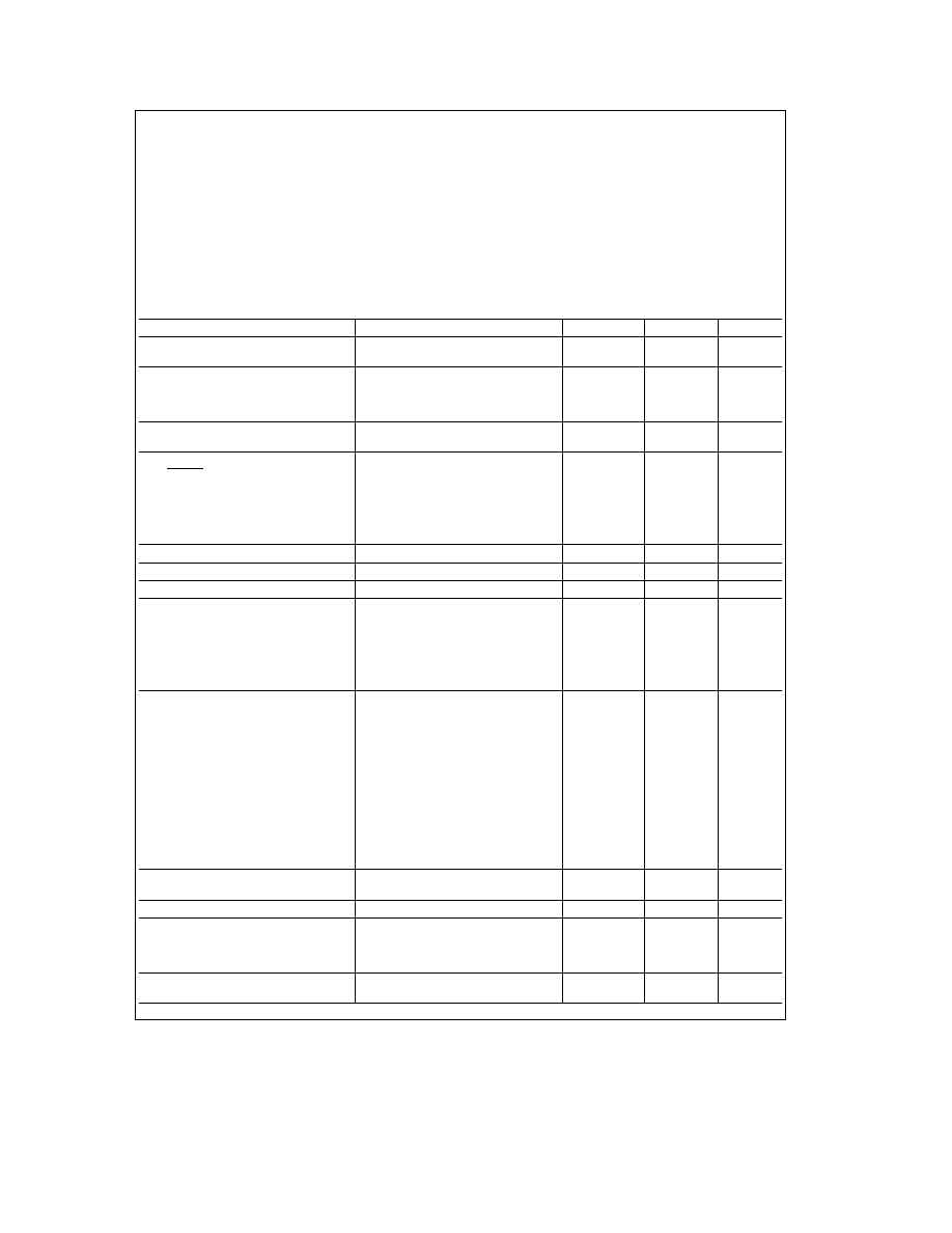
COP324C COP325C COP326C and COP344C COP345C
Absolute Maximum Ratings
Supply Voltage
6V
Voltage at any Pin
b
0 3V to V
CC
a
0 3V
Total Allowable Source Current
25 mA
Total Allowable Sink Current
25 mA
Operating Temperature Range
b
40 C to
a
85 C
Storage Temperature Range
b
65 C to
a
150 C
Lead Temperature
(soldering 10 seconds)
300 C
Note
Absolute maximum ratings indicate limits beyond
which damage to the device may occur DC and AC electri-
cal specifications are not ensured when operating the de-
vice at absolute maximum ratings
DC Electrical Characteristics
b
40 C
s
T
A
s
a
85 C unless otherwise specified
Parameter
Conditions
Min
Max
Units
Operating Voltage
3 0
5 5
V
Power Supply Ripple (Notes 4 5)
Peak to Peak
0 1 V
CC
V
Supply Current
V
CC
e
3 0V tc
e
64 ms
180
m
A
(Note 1)
V
CC
e
5 0V tc
e
16 ms
800
m
A
V
CC
e
5 0V tc
e
4 ms
3600
m
A
(tc is instruction cycle time)
HALT Mode Current
V
CC
e
5 0V F
IN
e
0 kHz
60
m
A
(Note 2)
V
CC
e
3 0V F
IN
e
0 kHz
30
m
A
Input Voltage Levels
RESET CKI D
O
(clock input)
Logic High
0 9 V
CC
V
Logic Low
0 1 V
CC
V
All Other Inputs
Logic High
0 7 V
CC
V
Logic Low
0 2 V
CC
V
Input Pull-Up Current
V
CC
e
4 5V V
IN
e
0
b
30
b
440
m
A
Hi-Z Input Leakage
b
2
a
2
m
A
Input Capacitance (Note 4)
7
pF
Output Voltage Levels
Standard Outputs
LSTTL Operation
V
CC
e
5 0V
g
10%
Logic High
I
OH
e b
100 mA
2 7
V
Logic Low
I
OL
e
400 mA
0 4
V
CMOS Operation
Logic High
I
OH
e b
10 mA
V
CC
b
0 2
V
Logic Low
I
OL
e
10 mA
0 2
V
Output Current Levels (except CKO)
Sink (Note 6)
V
CC
e
4 5V V
OUT
e
V
CC
1 2
mA
V
CC
e
3 0V V
OUT
e
V
CC
0 2
mA
Source (Standard Option)
V
CC
e
4 5V V
OUT
e
0V
b
0 5
mA
V
CC
e
3 0V V
OUT
e
0V
b
0 1
mA
Source (Low Current Option)
V
CC
e
4 5V V
OUT
e
0V
b
30
b
440
m
A
V
CC
e
3 0V V
OUT
e
0V
b
8
b
200
m
A
CKO Current Levels (As Clock Out)
Sink
d
4
0 3
mA
d
8
V
CC
e
4 5V CKI
e
V
CC
V
OUT
e
V
CC
0 6
mA
d
16
(
1 2
mA
Source
d
4
b
0 3
mA
d
8
V
CC
e
4 5V CKI
e
0V V
OUT
e
0V
b
0 6
mA
d
16
(
b
1 2
mA
Allowable Sink Source Current per
5
mA
Pin (Note 6)
Allowable Loading on CKO (as HALT)
100
pF
Current Needed to Over-Ride HALT
(Note 3)
To Continue
V
CC
e
4 5V V
IN
e
0 2V
CC
0 9
mA
To Halt
V
CC
e
4 5V V
IN
e
0 7V
CC
2 1
mA
TRI-STATE or Open Drain
Leakage Current
b
5
a
5
m
A
3
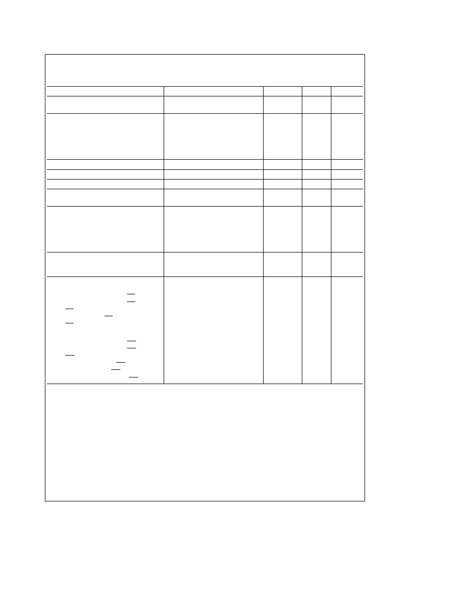
COP424C COP425C COP426C and COP444C COP445C
AC Electrical Characteristics
0 C
s
T
A
s
70 C unless otherwise specified
Parameter
Conditions
Min
Max
Units
Instruction Cycle Time (tc)
V
CC
t
4 5V
4
DC
m
s
4 5V
l
V
CC
t
2 4V
16
DC
m
s
Operating CKI
d
4 mode
DC
1 0
MHz
Frequency
d
8 mode
V
CC
t
4 5V
DC
2 0
MHz
d
16 mode
(
DC
4 0
MHz
d
4 mode
DC
250
kHz
d
8 mode
4 5V
l
V
CC
t
2 4V
DC
500
kHz
d
16 mode
(
DC
1 0
MHz
Duty Cycle (Note 4)
f
1
e
4 MHz
40
60
%
Rise Time (Note 4)
f
1
e
4 MHz External Clock
60
ns
Fall Time (Note 4)
f
1
e
4 MHz External Clock
40
ns
Instruction Cycle Time
R
e
30k
g
5% V
CC
e
5V
5
11
m
s
RC Oscillator (Note 4)
C
e
82 pF
g
5% (
d
4 Mode)
Inputs (See
Figure 3 )
t
SETUP
G Inputs
tc 4
a
7
m
s
SI Input
V
CC
t
4 5V
0 3
m
s
All Others
(
1 7
m
s
t
HOLD
V
CC
t
4 5V
0 25
m
s
4 5V
l
V
CC
t
2 4V
1 0
m
s
Output Propagation Delay
V
OUT
e
1 5V C
L
e
100 pF R
L
e
5k
t
PD1
t
PD0
V
CC
t
4 5V
1 0
m
s
t
PD1
t
PD0
4 5V
l
V
CC
t
2 4V
4 0
m
s
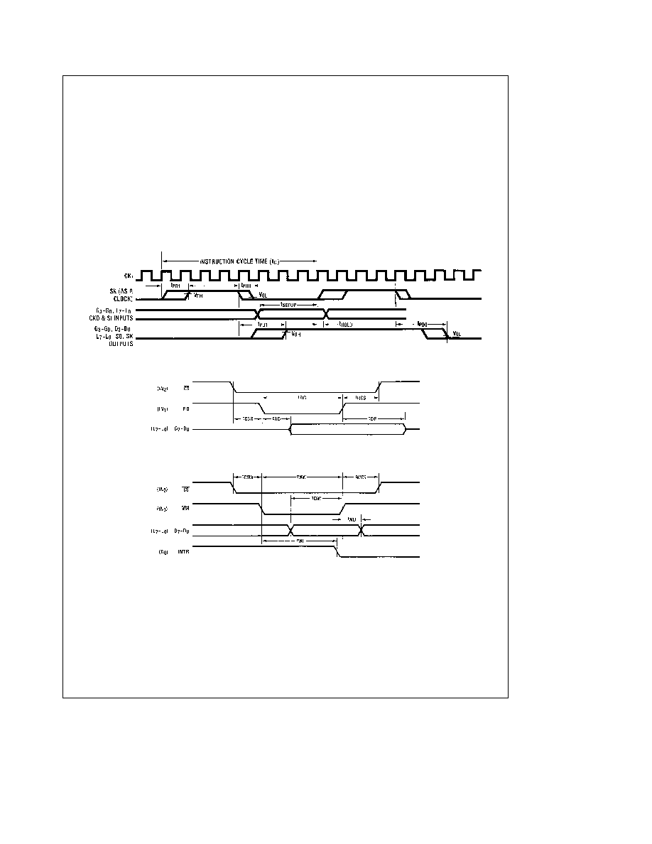
Microbus Timing
CL
e
50 pF V
CC
e
5V
g
5%
Read Operation (
Figure 4 )
Chip Select Stable before RD
b
t
CSR
65
ns
Chip Select Hold Time for RD
b
t
RCS
20
ns
RD Pulse Width
b
t
RR
400
ns
Data Delay from RD
b
t
RD
375
ns
RD to Data Floating
b
t
DF
(Note 4)
250
ns
Write Operation (
Figure 5 )
Chip Select Stable before WR
b
t
CSW
65
ns
Chip Select Hold Time for WR
b
t
WCS
20
ns
WR Pulse Width
b
t
WW
400
ns
Data Set-Up Time for WR
b
t
DW
320
ns
Data Hold Time for WR
b
t
WD
100
ns
INTR Transition Time from WR
b
t
WI
700
ns
Note 1
Supply current is measured after running for 2000 cycle times with a square-wave clock on CKI CKO open and all other pins pulled up to V
CC
with 5k
resistors See current drain equation on page 17
Note 2
The HALT mode will stop CKI from oscillating in the RC and crystal configurations Test conditions all inputs tied to V
CC
L lines in TRI-STATE mode and
tied to ground all outputs low and tied to ground
Note 3
When forcing HALT current is only needed for a short time (approx 200 ns) to flip the HALT flip-flop
Note 4
This parameter is only sampled and not 100% tested Variation due to the device included
Note 5
Voltage change must be less than 0 5 volts in a 1 ms period
Note 6
SO output sink current must be limited to keep V
OL
less than 0 2V
CC
when part is running in order to prevent entering test mode
4
COP324C COP325C COP326C and COP344C COP345C
AC Electrical Characteristics
b
40 C
s
T
A
s
a
85 C unless otherwise specified
Parameter
Conditions
Min
Max
Units
Instruction Cycle Time (tc)
V
CC
t
4 5V
4
DC
m
s
4 5V
l
V
CC
t
3 0V
16
DC
m
s
Operating CKI
d
4 mode
DC
1 0
MHz
Frequency
d
8 mode
V
CC
t
4 5V
DC
2 0
MHz
d
16 mode
(
DC
4 0
MHz
d
4 mode
DC
250
kHz
d
8 mode
4 5V
l
V
CC
t
3 0V
DC
500
kHz
d
16 mode
(
DC
1 0
MHz
Duty Cycle (Note 4)
f
1
e
4 MHz
40
60
%
Rise Time (Note 4)
f
1
e
4 MHz external clock
60
ns
Fall Time (Note 4)
f
1
e
4 MHz external clock
40
ns
Instruction Cycle Time
R
e
30k
g
5% V
CC
e
5V
5
11
m
s
RC Oscillator (Note 4)
C
e
82 pF
g
5% (
d
4 Mode)
Inputs (See
Figure 3 )
t
SETUP
G Inputs
tc 4
a
7
m
s
SI Inputs
V
CC
t
4 5V
0 3
m
s
All Others
(
1 7
m
s
t
HOLD
V
CC
t
4 5V
0 25
m
s
4 5V
l
V
CC
t
3 0V
1 0
m
s
Output Propagation Delay
V
OUT
e
1 5V C
L
e
100 pF R
L
e
5k
t
PD1
t
PD0
V
CC
t
4 5V
1 0
m
s
t
PD1
t
PD0
4 5V
l
V
CC
t
3 0V
4 0
m
s
Microbus Timing
C
L
e
50 pF V
CC
e
5V
g
5%
Read Operation (
Figure 4 )
Chip Select Stable before RD
b
t
CSR
65
ns
Chip Select Hold Time for RD
b
t
RCS
20
ns
RD Pulse Width
b
t
RR
400
ns
Data Delay from RD
b
t
RD
375
ns
RD to Data Floating
b
t
DF
(Note 4)
250
ns
Write Operation (
Figure 5 )
Chip Select Stable before WR
b
t
CSW
65
ns
Chip Select Hold Time for WR
b
t
WCS
20
ns
WR Pulse Width
b
t
WW
400
ns
Data Set-Up Time for WR
b
t
DW
320
ns
Data Hold Time for WR
b
t
WD
100
ns
INTR Transition Time from WR
b
t
WI
700
ns
Note 1
Supply current is measured after running for 2000 cycle times with a square-wave clock on CKI CKO open and all other pins pulled up to V
CC
with 5k
resistors See current drain equation on page 17
Note 2
The HALT mode will stop CKI from oscillating in the RC and crystal configurations Test conditions all inputs tied to V
CC
L lines in TRI-STATE mode and
tied to ground all outputs low and tied to ground
Note 3
When forcing HALT current is only needed for a short time (approx 200 ns) to flip the HALT flip-flop
Note 4
This parameter is only sampled and not 100% tested Variation due to the device included
Note 5
Voltage change must be less than 0 5 volts in a 1 ms period
Note 6
SO output sink current must be limited to keep V
OL
less than 0 2V
CC
when part is running in order to prevent entering test mode
5
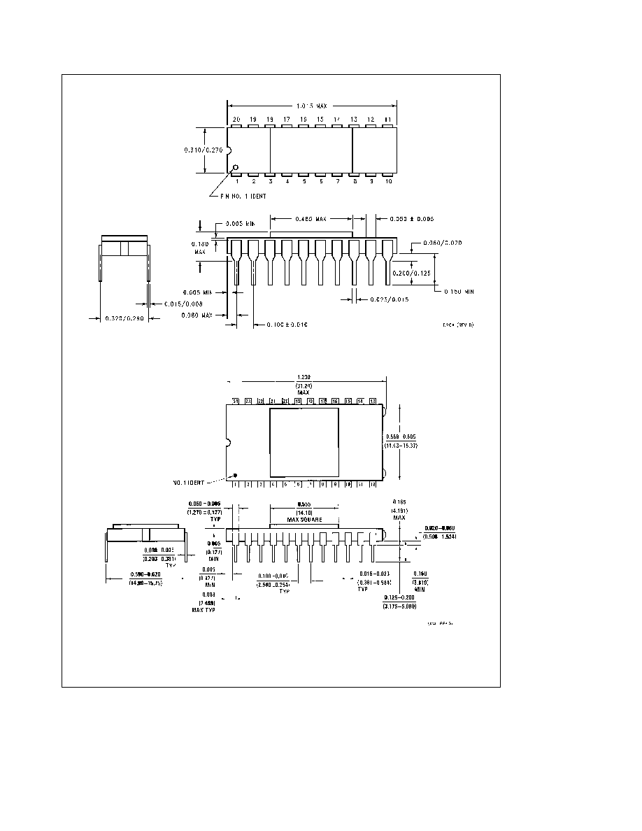
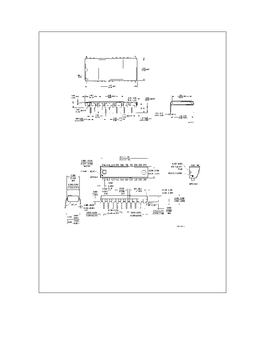
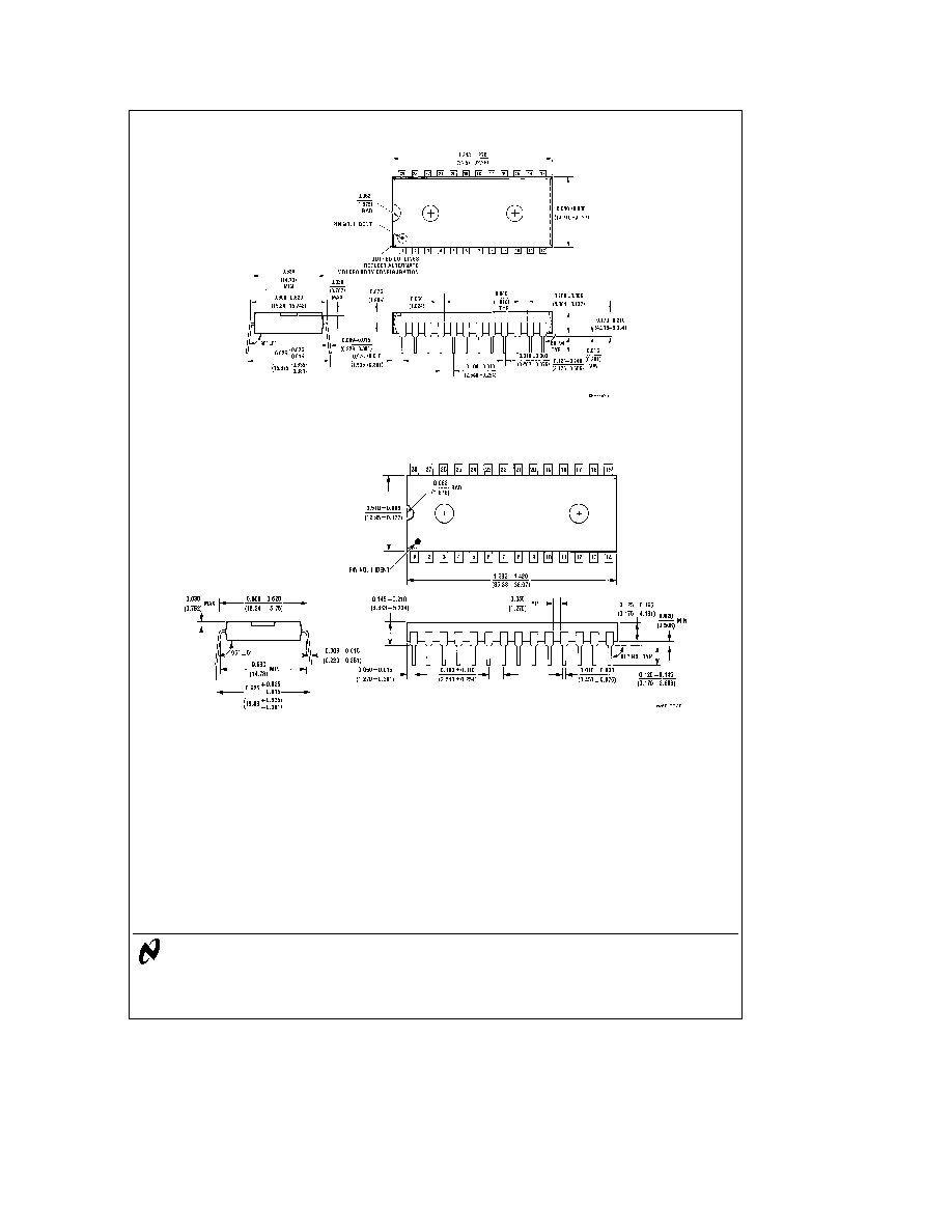
Connection Diagrams
DIP and S O Wide
TL DD 5259 � 16
Top View
Order Number COP326C-XXX D
or COP426C-XXX D
See NS Hermetic Package D20A
(Prototype Package Only)
Order Number COP326C-XXX N
or COP426C-XXX N
See NS Molded Package N20A
Order Number COP326C-XXX WM
or COP426C-XXX WM
See NS Surface Mount Package M20B
DIP and S O Wide
TL DD 5259 � 2
Top View
Order Number COP325C-XXX D COP445C-XXX D
COP425C-XXX D or COP345C-XXX D
See NS Hermetic Package D24C
(Prototype Package Only)
Order Number COP325C-XXX N COP345C-XXX N
COP425C-XXX N or COP445C-XXX N
See NS Molded Package N24A
Order Number COP325C-XXX WM COP345C-XXX WM
COP425C-XXX WM or COP445C-XXX WM
See NS Surface Mount Package M24B
Dual-In-Line Package
TL DD 5259 � 3
Top View
Order Number COP324C-XXX D COPC324-XXX WM COP344C-XXX D
COP424C-XXX D COPC424-XXX WM or COP444C-XXX D
See NS Hermetic Package D28C
(Prototype Package Only)
Order Number COP324C-XXX N COP344C-XXX N COPC344-XXX WM
COP424C-XXX N COP444C-XXX N or COPC444-XXX WM
See NS Molded Package N28B
FIGURE 2
Pin
Description
L7 � L0
8-bit bidirectional port with TRI-STATE
G3 � G0
4-bit bidirectional I O port
D3 � D0
4-bit output port
IN3 � IN0
4-bit input port (28-pin package only)
SI
Serial input or counter input
SO
Serial or general purpose output
Pin
Description
SK
Logic controlled clock output
CKI
Chip oscillator input
CKO
Oscillator output HALT I O port or general
purpose input
RESET
Reset input
V
CC
Most positive power supply
GND
Ground
6

Functional Description
The internal architecture is shown in
Figure 1 Data paths
are illustrated in simplified form to depict how the various
logic elements communicate with each other in implement-
ing the instruction set of the device Positive logic is used
When a bit is set it is a logic ``1'' when a bit is reset it is a
logic ``0''
For ease of reading only the COP424C 425C COP426C
444C 445C are referenced however all such references
apply equally to COP324C 325C COP326C 344C 345C
PROGRAM MEMORY
Program Memory consists of ROM 1024 bytes for the
COP424C 425C 426C and 2048 bytes for the COP444C
445C These bytes of ROM may be program instructions
constants or ROM addressing data
ROM addressing is accomplished by a 11-bit PC register
which selects one of the 8-bit words contained in ROM A
new address is loaded into the PC register during each in-
struction cycle Unless the instruction is a transfer of control
instruction the PC register is loaded with the next sequen-
tial 11-bit binary count value
Three levels of subroutine nesting are implemented by a
three level deep stack Each subroutine call or interrupt
pushes the next PC address into the stack Each return
pops the stack back into the PC register
DATA MEMORY
Data memory consists of a 512-bit RAM for the COP444C
445C organized as 8 data registers of 16
c
4-bit digits
RAM addressing is implemented by a 7-bit B register whose
upper 3 bits (Br) select 1 of 8 data registers and lower 4 bits
(Bd) select 1 of 16 4-bit digits in the selected data register
Data memory consists of a 256-bit RAM for the COP424C
425C 426C organized as 4 data registers of 16
c
4-bits
digits The B register is 6 bits long Upper 2 bits (Br) select 1
of 4 data registers and lower 4 bits (Bd) select 1 of 16 4-bit
digits in the selected data register While the 4-bit contents
of the selected RAM digit (M) are usually loaded into or
from or exchanged with the A register (accumulator) it
may also be loaded into or from the Q latches or T counter
or loaded from the L ports RAM addressing may also be
performed directly by the LDD and XAD instructions based
upon the immediate operand field of these instructions
The Bd register also serves as a source register for 4-bit
data sent directly to the D outputs
INTERNAL LOGIC
The processor contains its own 4-bit A register (accumula-
tor) which is the source and destination register for most I O
arithmetic logic and data memory access operations It can
also be used to load the Br and Bd portions of the B regis-
ter to load and input 4 bits of the 8-bit Q latch or T counter
to input 4 bits of L I O ports data to input 4-bit G or IN
ports and to perform data exchanges with the SIO register
A 4-bit adder performs the arithmetic and logic functions
storing the results in A It also outputs a carry bit to the 1-bit
C register most often employed to indicate arithmetic over-
flow The C register in conjunction with the XAS instruction
and the EN register also serves to control the SK output
The 8-bit T counter is a binary up counter which can be
loaded to and from M and A using CAMT and CTMA instruc-
tions When the T counter overflows an overflow flag will be
set (see SKT and IT instructions below) The T counter is
cleared on reset A functional block diagram of the timer
counter is illustrated in
Figure 10a
Four general-purpose inputs IN3-IN0 are provided IN1
IN2 and IN3 may be selected by a mask-programmable op-
tion as Read Strobe Chip Select and Write Strobe inputs
respectively for use in Microbus application
The D register provides 4 general-purpose outputs and is
used as the destination register for the 4-bit contents of Bd
In the dual clock mode D0 latch controls the clock selection
(see dual oscillator below)
The G register contents are outputs to a 4-bit general-pur-
pose bidirectional I O port G0 may be mask-programmed
as an output for Microbus applications
The Q register is an internal latched 8-bit register used to
hold data loaded to or from M and A as well as 8-bit data
from ROM Its contents are outputted to the L I O ports
when the L drivers are enabled under program control With
the Microbus option selected Q can also be loaded with the
8-bit contents of the L I O ports upon the occurrence of a
write strobe from the host CPU
The 8 L drivers when enabled output the contents of
latched Q data to the L I O port Also the contents of L may
be read directly into A and M As explained above the
Microbus option allows L I O port data to be latched into the
Q register
7
Functional Description
(Continued)
The SIO register functions as a 4-bit serial-in serial-out shift
register for MICROWIRE I O and COPS peripherals or as a
binary counter (depending on the contents of the EN regis-
ter) Its contents can be exchanged with A
The XAS instruction copies C into the SKL latch In the
counter mode SK is the output of SKL in the shift register
mode SK outputs SKL ANDed with the clock
EN is an internal 4-bit register loaded by the LEI instruction
The state of each bit of this register selects or deselects the
particular feature associated with each bit of the EN regis-
ter
0 The least significant bit of the enable register EN0 se-
lects the SIO register as either a 4-bit shift register or a
4-bit binary counter With EN0 set SIO is an asynchro-
nous binary counter decrementing its value by one upon
each low-going pulse (``1'' to ``0'') occurring on the SI
input Each pulse must be at least two instruction cycles
wide SK outputs the value of SKL The SO output equals
the value of EN3 With EN0 reset SIO is a serial shift
register left shifting 1 bit each instruction cycle time The
data present at SI goes into the least significant bit of
SIO SO can be enabled to output the most significant bit
of SIO each cycle time The SK outputs SKL ANDed with
the instruction cycle clock
1 With EN1 set interrupt is enabled Immediately following
an interrupt EN1 is reset to disable further interrupts
2 With EN2 set the L drivers are enabled to output the data
in Q to the L I O port Resetting EN2 disables the L driv-
ers placing the L I O port in a high-impedance input
state
TL DD 5259 � 4
FIGURE 3 Input Output Timing Diagrams (divide by 8 mode)
TL DD 5259 � 5
FIGURE 4 Microbus Read Operation Timing
TL DD 5259 � 6
FIGURE 5 Microbus Write Operation Timing
8
Functional Description
(Continued)
3 EN3 in conjunction with EN0 affects the SO output With
EN0 set (binary counter option selected) SO will output
the value loaded into EN3 With EN0 reset (serial shift
register option selected) setting EN3 enables SO as the
output of the SIO shift register outputting serial shifted
data each instruction time Resetting EN3 with the serial
shift register option selected disables SO as the shift reg-
ister output data continues to be shifted through SIO and
can be exchanged with A via an XAS instruction but SO
remains set to ``0''
INTERRUPT
The following features are associated with interrupt proce-
dure and protocol and must be considered by the program-
mer when utilizing interrupts
a The interrupt
once recognized as explained below
pushes the next sequential program counter address
(PC
a
1) onto the stack Any previous contents at the bot-
tom of the stack are lost The program counter is set to
hex address 0FF (the last word of page 3) and EN1 is
reset
b An interrupt will be recognized only on the following con-
ditions
1 EN1 has been set
2 A low-going pulse (``1'' to ``0'') at least two instruction
cycles wide has occurred on the IN
1
input
3 A currently executing instruction has been completed
4 All successive transfer of control instructions and suc-
cessive LBIs have been completed (e g if the main
program is executing a JP instruction which transfers
program control to another JP instruction the interrupt
will not be acknowledged until the second JP instruc-
tion has been executed)
c Upon acknowledgement of an interrupt the skip logic
status is saved and later restored upon popping of the
stack For example if an interrupt occurs during the exe-
cution of ASC (Add with Carry Skip on Carry) instruction
which results in carry the skip logic status is saved and
program control is transferred to the interrupt servicing
routine at hex address 0FF At the end of the interrupt
routine a RET instruction is executed to pop the stack
and return program control to the instruction following the
original ASC At this time the skip logic is enabled and
skips this instruction because of the previous ASC carry
Subroutines should not be nested within the interrupt
service routine since their popping of the stack will en-
able any previously saved main program skips interfering
with the orderly execution of the interrupt routine
d The instruction at hex address 0FF must be a NOP
e An LEI instruction may be put immediately before the
RET instruction to re-enable interrupts
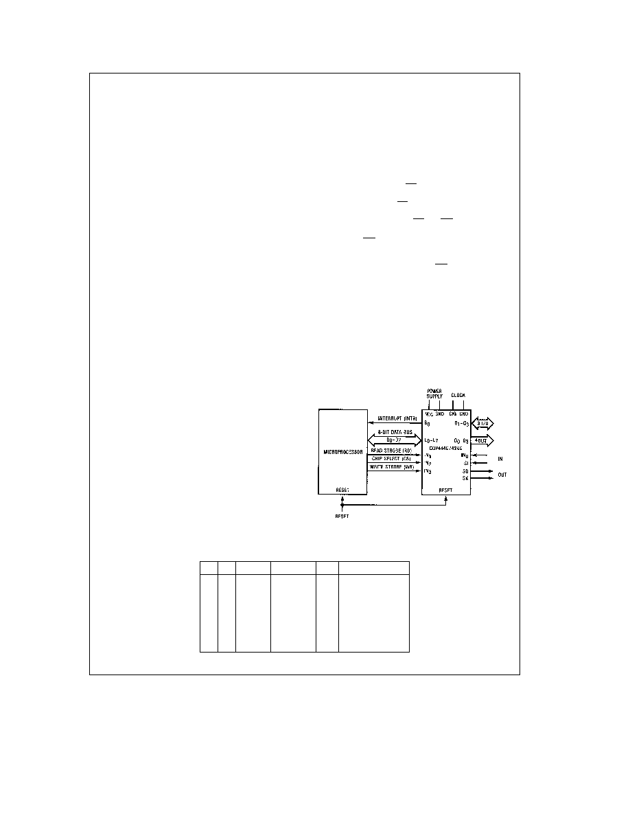
MICROBUS INTERFACE
The COP444C 424C has an option which allows it to be
used as a peripheral microprocessor device inputting and
outputting data from and to a host microprocessor (mP)
IN1 IN2 and IN3 general purpose inputs become Microbus
compatible read-strobe chip-select and write-strobe lines
respectively IN1 becomes RD
a logic ``0'' on this input
will cause Q latch data to be enabled to the L ports for input
to the uP IN2 becomes CS
a logic ``0'' on this line se-
lects the COP444C 424C as the uP peripheral device by
enabling the operation of the RD and WR lines and allows
for the selection of one of several peripheral components
IN3 becomes WR
a logic ``0'' on this line will write bus
data from the L ports to the Q latches for input to the
COP444C 424C G0 becomes INTR a ``ready'' output reset
by a write pulse from the uP on the WR line providing the
``handshaking'' capability necessary for asynchronous data
transfer between the host CPU and the COP444C 424C
This option has been designed for compatibility with Nation-
al's Microbus
a standard interconnect system for 8-bit
parallel data transfer between MOS LSI CPUs and interfac-
ing devices (See Microbus National Publication ) The func-
tioning and timing relationships between the signal lines af-
fected by this option are as specified for the Microbus inter-
face and are given in the AC electrical characteristics and
shown in the timing diagrams (
Figures 4 and 5 ) Connection
of the COP444C 424C to the Microbus is shown in
Figure 6
TL DD 5259 � 7
FIGURE 6 Microbus Option Interconnect
TABLE I Enable Register Modes
Bits EN0 and EN3
EN0 EN3
SIO
SI
SO
SK
0
0
Shift
Input to Shift
0
If SKL
e
1 SK
e
clock
Register
Register
If SKL
e
0 SK
e
0
0
1
Shift
Input to Shift Serial If SKL
e
1 SK
e
clock
Register
Register
out
If SKL
e
0 SK
e
0
1
0
Binary
Input to
0
SK
e
SKL
Counter
Counter
1
1
Binary
Input to
1
SK
e
SKL
Counter
Counter
9
Functional Description
(Continued)
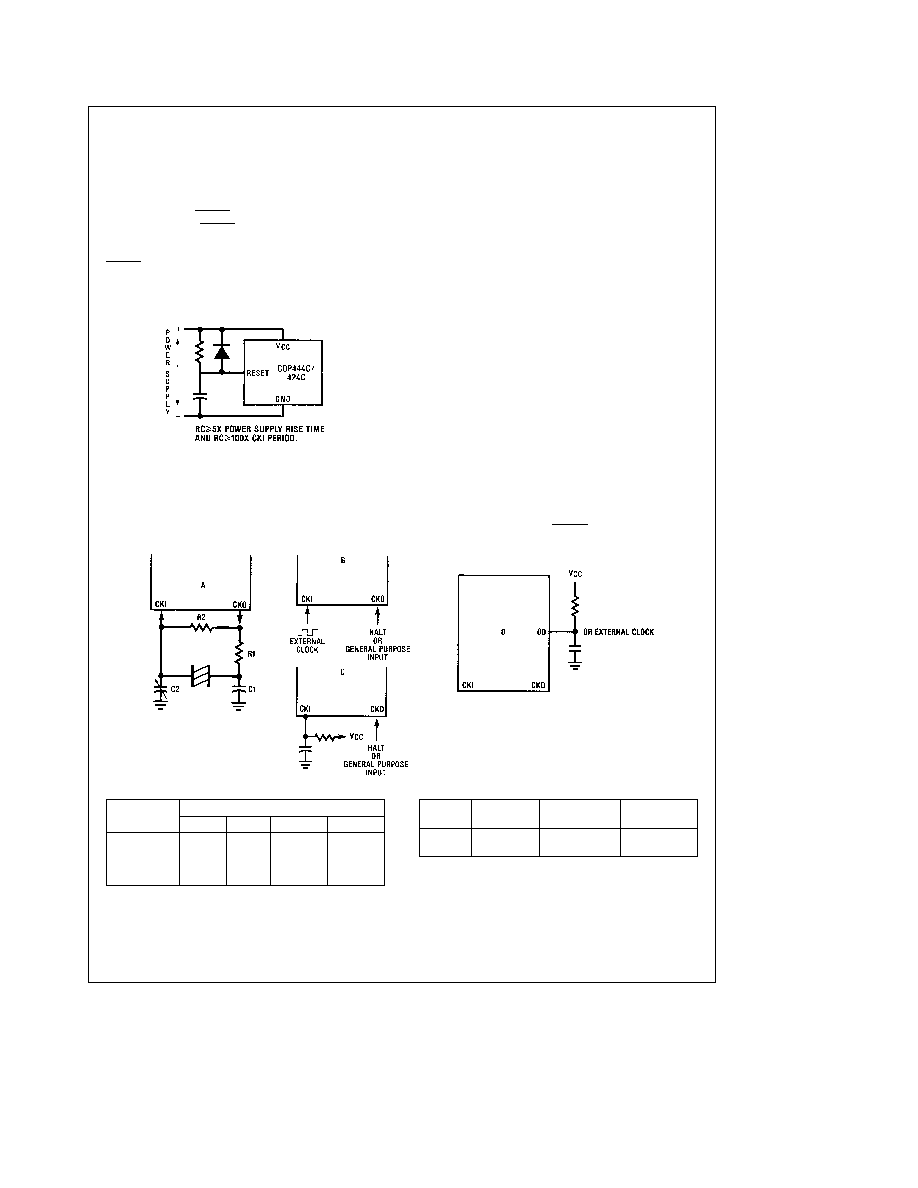
INITIALIZATION
The internal reset logic will initialize the device upon power-
up if the power supply rise time is less than 1 ms and if the
operating frequency at CKI is greater than 32 kHz other-
wise the external RC network shown in
Figure 7 must be
connected to the RESET pin (the conditions in
Figure 7
must be met) The RESET pin is configured as a Schmitt
trigger input If not used it should be connected to V
CC
Initialization will occur whenever a logic ``0'' is applied to the
RESET input providing it stays low for at least three instruc-
tion cycle times
Note
If CKI clock is less than 32 kHz the internal reset logic (option
29
e
1) MUST be disabled and the external RC circuit must be used
TL DD 5259 � 8
FIGURE 7 Power-Up Circuit
Upon initialization the PC register is cleared to 0 (ROM ad-
dress 0) and the A B C D EN IL T and G registers are
cleared The SKL latch is set thus enabling SK as a clock
output Data Memory (RAM) is not cleared upon initializa-
tion The first instruction at address 0 must be a CLRA
(clear A register)
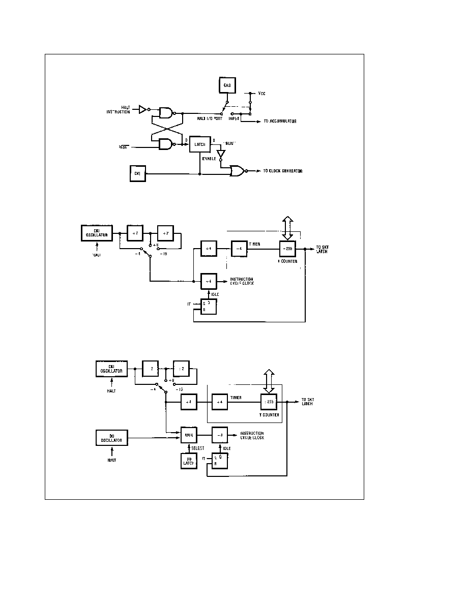
TIMER
The timer can be operated as a time-base counter
The instruction cycle frequency generated from CKI passes
through a 2-bit divide-by-4 prescaler The output of this pre-
scaler increments the 8-bit T counter thus providing a 10-bit
timer The pre-scaler is cleared during execution of a CAMT
instruction and on reset
For example using a 4 MHz crystal with a divide-by-16 op-
tion the instruction cycle frequency of 250 kHz increments
the 10-bit timer every 4 ms By presetting the counter and
detecting overflow
accurate timeouts between 16 ms
(4 counts) and 4 096 ms (1024 counts) are possible Longer
timeouts can be achieved by accumulating under software
control multiple overflows
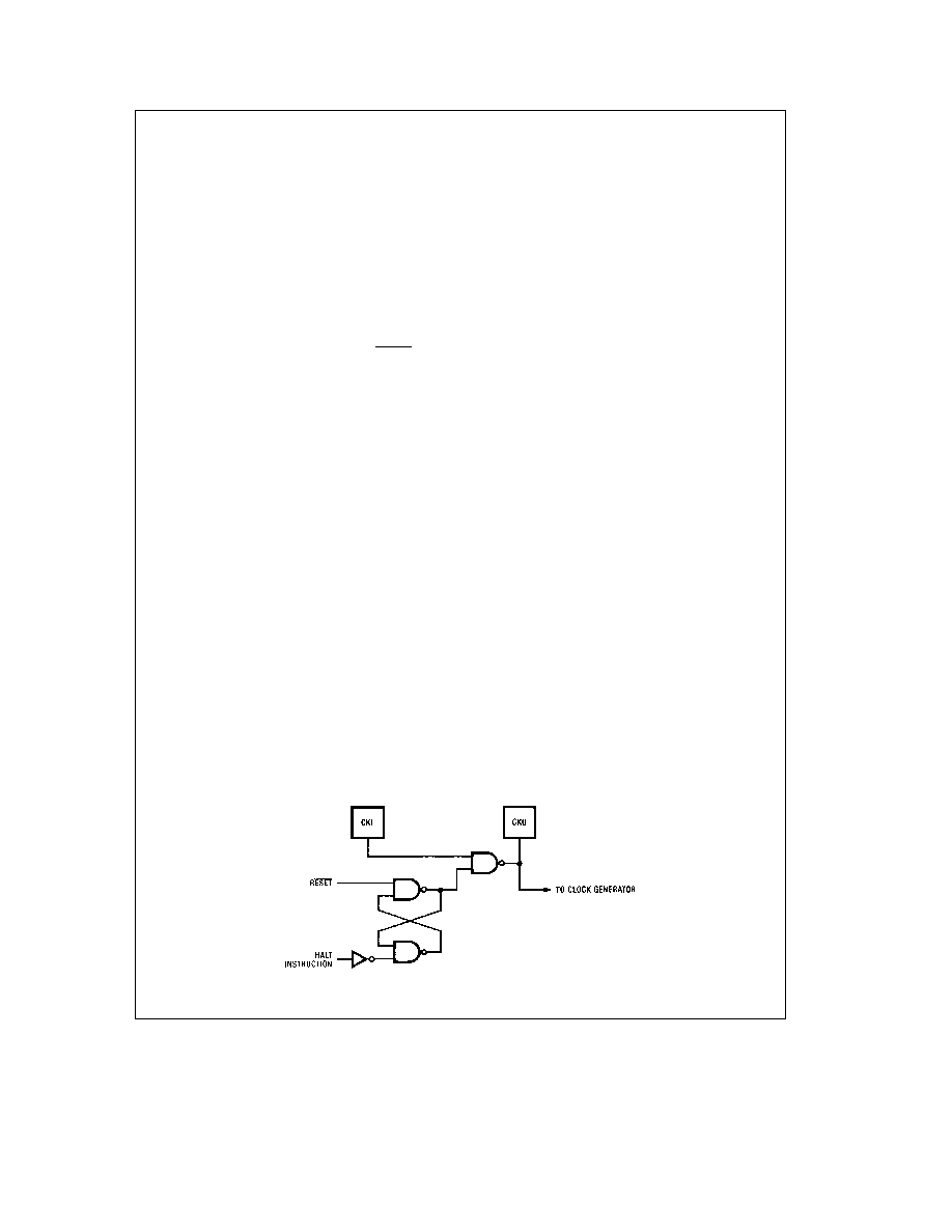
HALT MODE
The COP444C 445C 424C 425C 426C is a FULLY STAT-
IC circuit therefore the user may stop the system oscillator
at any time to halt the chip The chip may also be halted by
the HALT instruction or by forcing CKO high when it is
mask-programmed as an HALT I O port Once in the HALT
mode the internal circuitry does not receive any clock sig-
nal and is therefore frozen in the exact state it was in when
halted All information is retained until continuing The chip
may be awakened by one of two different methods
Continue function by forcing CKO low if it mask-pro-
grammed as an HALT I O port the system clock is re-
enabled and the circuit continues to operate from the
point where it was stopped
Restart by forcing the RESET pin low (see Initializa-
tion)
TL DD 5259 � 9
Crystal or Resonator
Crystal
Component Values
Value
R1
R2
C1(pF)
C2(pF)
32 kHz
220k
20M
30
6 � 36
455 kHz
5k
10M
80
40
2 096 MHz
2k
1M
30
6 � 36
4 0 MHz
1k
1M
30
6 � 36
RC Controlled Oscillator (
g
5% R
g
5% C)
R
C
Cycle
V
CC
Time
30k
82 pF
5 � 11 ms
t
4 5V
60k
100 pF
12 � 24 ms
2 4 � 4 5V
Note
15k
s
R
s
150k
50 pF
s
C
s
150 pF
FIGURE 8 Oscillator Component Values
10
Functional Description
(Continued)
The HALT mode is the minimum power dissipation state
Note If the user has selected dual-clock with D0 as external
oscillator (option 30
e
2) AND the COP444C 424C is
running with the D0 clock the HALT mode
either
hardware or software
will NOT be entered Thus
the user should switch to the CKI clock to HALT Al-
ternatively the user may stop the D0 clock to mini-
mize power
CKO PIN OPTIONS
a Two-pin oscillator
(Crystal) See
Figure 9A
In a crystal controlled oscillator system CKO is used as
an output to the crystal network The HALT mode may be
entered by program control (HALT instruction) which
forces CKO high thus inhibiting the crystal network The
circuit can be awakened only by forcing the RESET pin to
a logic ``0'' (restart)
b One-pin oscillator
(RC or external) See
Figure 9B
If a one-pin oscillator system is chosen two options are
available for CKO
CKO can be selected as the HALT I O port In that
case it is an I O flip-flop which is an indicator of the
HALT status An external signal can over-ride this pin
to start and stop the chip By forcing a high level to
CKO the chip will stop as soon as CKI is high and
CKO output will stay high to keep the chip stopped if
the external driver returns to high impedance state
By forcing a low level to CKO the chip will continue
and CKO will stay low
As another option CKO can be a general purpose in-
put read into bit 2 of A (accumulator) upon execution
of an INIL instruction
OSCILLATOR OPTIONS
There are four basic clock oscillator configurations available
as shown by
Figure 8
a Crystal Controlled Oscillator CKI and CKO are connect-
ed to an external crystal The instruction cycle time equals
the crystal frequency optionally divided by 4 8 or 16
b External Oscillator The external frequency is optionally
divided by 4 8 or 16 to give the instruction cycle time
CKO is the HALT I O port or a general purpose input
c RC Controlled Oscillator CKI is configured as a single pin
RC controlled Schmitt trigger oscillator The instruction
cycle equals the oscillation frequency divided by 4 CKO
is the HALT I O port or a general purpose input
d Dual oscillator By selecting the dual clock option pin D0
is now a single pin oscillator input Two configurations are
available RC controlled Schmitt trigger oscillator or exter-
nal oscillator
The user may software select between the D0 oscillator
(in that case the instruction cycle time equals the D0
oscillation frequency divided by 4) by setting the D0 latch
high or the CKI (CKO) oscillator by resetting D0 latch low
Note that even in dual clock mode the counter if mask-
programmed as a time-base counter is always connect-
ed to the CKI oscillator
For example the user may connect up to a 1 MHz RC
circuit to D0 for faster processing and a 32 kHz watch
crystal to CKI and CKO for minimum current drain and
time keeping
Note CTMA instruction is not allowed when chip is running
from D0 clock
Figures 10A and 10B show the clock and timer diagrams
with and without Dual clock
COP445C AND COP425C 24-PIN PACKAGE OPTION
If the COP444C 424C is bonded in a 24-pin package it be-
comes the COP445C 425C illustrated in
Figure 2 Connec-
tion diagrams Note that the COP445C 425C does not con-
tain the four general purpose IN inputs (IN3 � IN0) Use of
this option precludes of course use of the IN options in-
terrupt feature external event counter feature and the
Microbus option which uses IN1 � IN3 All other options are
available for the COP445C 425C
Note If user selects the 24-pin package options 9 10 19
and 20 must be selected as a ``0'' (load to V
CC
on the
IN inputs) See option list
COP426C 20-PIN PACKAGE OPTION
If the COP425C is bonded as 20-pin device it becomes the
COP426C
Note that the COP426C contains all the
COP425C pins except D
0
D
1
G
0
and G
1
Block Diagram
(Continued)
TL DD 5259 � 10
FIGURE 9A Halt Mode
Two-Pin Oscillator
11
Block Diagram
(Continued)
TL DD 5259 � 11
FIGURE 9B Halt Mode
One-Pin Oscillator
TL DD 5259 � 12
FIGURE 10A Clock and Timer without Dual-Clock
TL DD 5259 � 13
FIGURE 10B Clock and Timer with Dual-Clock
12
Instruction Set
Table II is a symbol table providing internal architecture in-
struction operan and operation symbols used in the instruc-
tion set table
TABLE II Instruction Set Table Symbols
Symbol
Definition
Internal Architecture Symbols
A
4-bit accumulator
B
7-bit RAM address register (6-bit for COP424C)
Br
Upper 3 bits of B (register address)
(2-bit for COP424C)
Bd
Lower 4 bits of B (digit address)
C
1-bit carry register
D
4-bit data output port
EN
4-bit enable register
G
4-bit general purpose I O port
IL
two 1-bit (IN0 and IN3) latches
IN
4-bit input port
L
8-bit TRI-STATE I O port
M
4-bit contents of RAM addressed by B
PC
11-bit ROM address program counter
Q
8-bit latch for L port
SA SB SC 11-bit 3-level subroutine stack
SIO
4-bit shift register and counter
SK
Logic-controlled clock output
SKL
1-bit latch for SK output
T
8-bit timer
Table III provides the mnemonic operand machine code
data flow skip conditions and description of each instruc-
tion
Instruction Operand Symbols
d
4-bit operand field 0 � 15 binary (RAM digit select)
r
3(2)-bit operand field 0 � 7(3) binary
(RAM register select)
a
11-bit operand field 0 � 2047 (1023)
y
4-bit operand field 0 � 15 (immediate data)
RAM(x) RAM addressed by variable x
ROM(x) ROM addressed by variable x
Operational Symbols
a
Plus
b
Minus
x
Replaces
Is exchanged with
e
Is equal to
A
One's complement of A
Z
Exclusive-or
Range of values
TABLE III COP444C 445C Instruction Set
Machine
Mnemonic
Operand
Hex
Language
Data Flow
Skip
Description
Code
Code
Conditions
(Binary)
ARITHMETIC INSTRUCTIONS
ASC
30
0011 0000
A
a
C
a
RAM(B)
x
A
Carry
Add with Carry Skip on
Carry
x
C
Carry
ADD
31
0011 0001
A
a
RAM(B)
x
A
None
Add RAM to A
ADT
4A
0100 1010
A
a
10
10
x
A
None
Add Ten to A
AISC
y
5
b
0101
y
A
a
y
x
A
Carry
Add Immediate Skip on
Carry (y
i
0)
CASC
10
0001 0000
A
a
RAM(B)
a
C
x
A
Carry
Complement and Add with
Carry
x
C
Carry Skip on Carry
CLRA
00
0000 0000
0
x
A
None
Clear A
COMP
40
0100 0000
A
x
A
None
Ones complement of A to A
NOP
44
0100 0100
None
None
No Operation
RC
32
0011 0010
``0''
x
C
None
Reset C
SC
22
0010 0010
``1''
x
C
None
Set C
XOR
02
0000 0010
A
Z
RAM(B)
x
A
None
Exclusive-OR RAM with A
13
Instruction Set
(Continued)
Table III COP444C 445C Instruction Set
(Continued)
Machine
Mnemonic
Operand
Hex
Language
Data Flow
Skip
Description
Code
Code
Conditions
(Binary)
TRANSFER CONTROL INSTRUCTIONS
JID
FF
1111 1111
ROM (PC
10 8
A M)
x
PC
7 0
None
Jump Indirect (Notes 1 3)
JMP
a
6
b
0110 0 a
10 8
a
x
PC
None
Jump
b b
a
7 0
JP
a
b b
1
a
6 0
a
x
PC
6 0
None
Jump within Page (Note 4)
(pages 2 3 only)
or
b b
11
a
5 0
a
x
PC
5 0
(all other pages)
JSRP
a
b b
10
a
5 0
PC
a
1
x
SA
x
SB
x
SC
None
Jump to Subroutine Page
00010
x
PC
10 6
(Note 5)
a
x
PC
5 0
JSR
a
6
b
0110 1 a
10 8
PC
a
1
x
SA
x
SB
x
SC
None
Jump to Subroutine
b b
a
7 0
a
x
PC
RET
48
0100 1000
SC
x
SB
x
SA
x
PC
None
Return from Subroutine
RETSK
49
0100 1001
SC
x
SB
x
SA
x
PC
Always Skip
Return from Subroutine
on Return
then Skip
HALT
33
0011 0011
None
HALT Processor
38
0011 1000
IT
33
0011 0011
IDLE till Timer
39
0011 1001
None
Overflows then Continues
MEMORY REFERENCE INSTRUCTIONS
CAMT
33
0011 0011
A
x
T
7 4
3F
0011 1111
RAM(B)
x
T
3 0
None
Copy A RAM to T
CTMA
33
0011 0011
T
7 4
x
RAM(B)
2F
0010 1111
T
3 0
x
A
None
Copy T to RAM A (Note 9)
CAMQ
33
0011 0011
A
x
Q
7 4
None
Copy A RAM to Q
3C
0011 1100
RAM(B)
x
Q
3 0
CQMA
33
0011 0011
Q
7 4
x
RAM(B)
None
Copy Q to RAM A
2C
0010 1100
Q
3 0
x
A
LD
r
b
5
00 r 0101
RAM(B)
x
A
None
Load RAM into A
(r
e
0 3)
Br
Z
r
x
Br
Exclusive-OR Br with r
LDD
r d
23
0010 0011
RAM(r d)
x
A
None
Load A with RAM pointed
b b
0
r
d
to directly by r d
LQID
BF
1011 1111
ROM(PC
10 8
A M)
x
Q
None
Load Q Indirect (Note 3)
SB
x
SC
RMB
0
4C
0100 1100
0
x
RAM(B)
0
None
Reset RAM Bit
1
45
0100 0101
0
x
RAM(B)
1
2
42
0100 0010
0
x
RAM(B)
2
3
43
0100 0011
0
x
RAM(B)
3
SMB
0
4D
0100 1101
1
x
RAM(B)
0
None
Set RAM Bit
1
47
0100 0111
1
x
RAM(B)
1
2
46
0100 0110
1
x
RAM(B)
2
3
4B
0100 1011
1
x
RAM(B)
3
14
Instruction Set
(Continued)
Table III COP444C 445C Instruction Set
(Continued)
Machine
Mnemonic
Operand
Hex
Language
Data Flow
Skip
Description
Code
Code
Conditions
(Binary)
MEMORY REFERENCE INSTRUCTIONS
(Continued)
STII
y
7
b
0111
y
y
x
RAM(B)
None
Store Memory Immediate
Bd
a
1
x
Bd
1 and Increment Bd
X
r
b
6
00
r
0110
RAM(B)
A
None
Exchange RAM with A
(r
e
0 3)
Br
Z
r
x
Br
Exclusive-OR Br with r
XAD
r d
23
0010 0011
RAM(r d)
A
None
Exchange A with RAM
b b
1 r
d
Pointed to Directly by r d
XDS
r
b
7
00 r 0111
RAM(B)
A
Bd
Exchange RAM with A
(r
e
0 3)
Bd
b
1
x
Bd
decrements
and Decrement Bd
Br
Z
r
x
Br
past 0
Exclusive-OR Br with r
XIS
r
b
4
00
r
0100
RAM(B)
A
Bd
Exchange RAM with A
(r
e
0 3)
Bd
a
1
x
Bd
increments
and Increment Bd
Br
Z
r
x
Br
past 15
Exclusive-OR Br with r
REGISTER REFERENCE INSTRUCTIONS
CAB
50
0101 0000
A
x
Bd
None
Copy A to Bd
CBA
4E
0100 1110
Bd
x
A
None
Copy Bd to A
LBI
r d
b b
00 r (d � 1)
r d
x
B
Skip until
Load B Immediate with r d
(r
e
0 3
not a LBI
(Note 6)
d
e
0 9 15)
or
33
0011 0011
b b
1
r
d
(any r any d)
LEI
y
33
0011 0011
y
x
EN
None
Load EN Immediate (Note 7)
6
b
0110
y
XABR
12
0001 0010
A
Br
None
Exchange A with Br (Note 8)
TEST INSTRUCTIONS
SKC
20
0010 0000
C
e
``1''
Skip if C is True
SKE
21
0010 0001
A
e
RAM(B)
Skip if A Equals RAM
SKGZ
33
0011 0011
G
3 0
e
0
Skip if G is Zero
21
0010 0001
(all 4 bits)
SKGBZ
33
0011 0011
1st byte
Skip if G Bit is Zero
0
01
0000 0001
G
0
e
0
1
11
0001 0001
G
1
e
0
2
03
0000 0011
2nd byte
G
2
e
0
3
13
0001 0011
*
G
3
e
0
SKMBZ
0
01
0000 0001
RAM(B)
0
e
0
Skip if RAM Bit is Zero
1
11
0001 0001
RAM(B)
1
e
0
2
03
0000 0011
RAM(B)
2
e
0
3
13
0001 0011
RAM(B)
3
e
0
SKT
41
0100 0001
A time-base
Skip on Timer
counter carry
(Note 3)
has occurred
since last test
15
Instruction Set
(Continued)
Table III COP444C 445C Instruction Set
(Continued)
Machine
Mnemonic
Operand
Hex
Language
Data Flow
Skip
Description
Code
Code
Conditions
(Binary)
INPUT OUTPUT INSTRUCTIONS
ING
33
0011 0011
G
x
A
None
Input G Ports to A
2A
0010 1010
ININ
33
0011 0011
IN
x
A
None
Input IN Inputs to A
28
0010 1000
(Note 2)
INIL
33
0011 0011
IL
3
CKO ``0'' IL
0
x
A
None
Input IL Latches to A
29
0010 1001
(Note 3)
INL
33
0011 0011
L
7 4
x
RAM(B)
None
Input L Ports to RAM A
2E
0010 1110
L
3 0
x
A
OBD
33
0011 0011
Bd
x
D
None
Output Bd to D Outputs
3E
0011 1110
OGI
y
33
0011 0011
y
x
G
None
Output to G Ports
5
b
0101
y
Immediate
OMG
33
0011 0011
RAM(B)
x
G
None
Output RAM to G Ports
3A
0011 1010
XAS
4F
0100 1111
A
SIO C
x
SKL
None
Exchange A with SIO
(Note 3)
Note 1
All subscripts for alphabetical symbols indicate bit numbers unless explicitly defined (e g Br and Bd are explicitly defined) Bits are numbered 0 to N where
0 signifies the least significant bit (low-order right-most bit) For example A
3
indicates the most significant (left-most) bit of the 4-bit A register
Note 2
The ININ instruction is not available on the 24-pin packages since these devices do not contain the IN inputs
Note 3
For additional information on the operation of the XAS JID LQID INIL and SKT instructions see below
Note 4
The JP instruction allows a jump while in subroutine pages 2 or 3 to any ROM location within the two-page boundary of pages 2 or 3 The JP instruction
otherwise permits a jump to a ROM location within the current 64-word page JP may not jump to the last word of a page
Note 5
A JSRP transfers program control to subroutine page 2 (0010 is loaded into the upper 4 bits of P) A JSRP may not be used when in pages 2 or 3 JSRP
may not jump to the last word in page 2
Note 6
LBI is a single-byte instruction if d
e
0 9 10 11 12 13 14 or 15 The machine code for the lower 4 bits equals the binary value of the ``d'' data
minus 1
e g to load the lower four bits of B(Bd) with the value 9 (1001
2
) the lower 4 bits of the LBI instruction equal 8 (1000
2
) To load 0 the lower 4 bits of the LBI
instruction should equal 15 (1111
2
)
Note 7
Machine code for operand field y for LEI instruction should equal the binary value to be latched into EN where a ``1'' or ``0'' in each bit of EN corresponds
with the selection or deselection of a particular function associated with each bit (See Functional Description EN Register )
Note 8
For 2K ROM devices A
Br (0
x
A3) For 1K ROM devices A
Br (0 0
x
A3 A2)
Note 9
Do not use CTMA instruction when dual-clock option is selected and part is running from D
0
clocks
16

Description of Selected Instructions
XAS INSTRUCTION
XAS (Exchange A with SIO) copies C to the SKL latch and
exchanges the accumulator with the 4-bit contents of the
SIO register The contents of SIO will contain serial-in seri-
al-out shift register or binary counter data depending on the
value of the EN register If SIO is selected as a shift register
an XAS instruction can be performed once every 4 instruc-
tion cycles to effect a continuous data stream
LQID INSTRUCTION
LQID (Load Q Indirect) loads the 8-bit Q register with the
contents
of
ROM
pointed
to
by
the
11-bit
word
PC10 PC8 A M LQID can be used for table lookup or code
conversion such as BCD to seven-segment The LQID in-
struction ``pushes'' the stack (PC
a
1
x
SA
x
SB
x
SC)
and replaces the least significant 8 bits of the PC as follows
A
x
PC(7 4) RAM(B)
x
PC(3 0) leaving PC(10) PC(9)
and PC(8) unchanged The ROM data pointed to by the new
address is fetched and loaded into the Q latches Next the
stack is ``popped'' (SC
x
SB
x
SA
x
PC) restoring the
saved value of PC to continue sequential program execu-
tion Since LQID pushes SB
x
SC the previous contents
of SC are lost
Note
LQID uses 2 instruction cycles if executed one if skipped
JID INSTRUCTION
JID (Jump Indirect) is an indirect addressing instruction
transferring program control to a new ROM location pointed
to indirectly by A and M It loads the lower 8 bits of the ROM
address register PC with the contents of ROM addressed by
the 11-bit word PC10 8 A M PC10 PC9 and PC8 are not
affected by JID
Note
JID uses 2 instruction cycles if executed one if skipped
SKT INSTRUCTION
The SKT (Skip On Timer) instruction tests the state of the T
counter overflow latch (see internal logic above) executing
the next program instruction if the latch is not set If the
latch has been set since the previous test the next program
instruction is skipped and the latch is reset The features
associated with this instruction allow the processor to gen-
erate its own time-base for real-time processing rather than
relying on an external input signal
Note
If the most significant bit of the T counter is a 1 when a CAMT instruc-
tion loads the counter the overflow flag will be set The following
sample of codes should be used when loading the counter
load T counter
CAMT
skip if overflow flag is set and reset it
SKT
NOP
IT INSTRUCTION
The IT (idle till timer) instruction halts the processor and
puts it in an idle state until the time-base counter overflows
This idle state reduces current drain since all logic (except
the oscillator and time base counter) is stopped
INIL INSTRUCTION
INIL (Input IL Latches to A) inputs 2 latches IL3 and IL0
CKO and 0 into A The IL3 and IL0 latches are set if a low-
going pulse (``1'' to ``0'') has occurred on the IN3 and IN0
inputs since the last INIL instruction provided the input
pulse stays low for at least two instruction cycles Execution
of an INIL inputs IL3 and IL0 into A3 and A0 respectively
and resets these latches to allow them to respond to subse-
quent low-going pulses on the IN3 and IN0 lines If CKO is
mask programmed as a general purpose input an INIL will
input the state of CKO into A2 If CKO has not been so
programmed a ``1'' will be placed in A2 A0 is input into A1
IL latches are cleared on reset IL latches are not available
on the COP445C 425C and COP426C
INSTRUCTION SET NOTES
a The first word of a program (ROM address 0) must be a
CLRA (Clear A) instruction
b Although skipped instructions are not executed they are
still fetched from the program memory Thus program
paths take the same number of cycles whether instruc-
tions are skipped or executed except for JID and LQID
c The ROM is organized into pages of 64 words each The
Program Counter is a 11-bit binary counter and will count
through page boundaries If a JP JSRP JID or LQID is
the last word of a page it operates as if it were in the next
page For example a JP located in the last word of a
page will jump to a location in the next page Also a JID
or LQID located in the last word of every fourth page (i e
hex address 0FF 1FF 2FF 3FF 4FF etc ) will access
data in the next group of four pages
Note
The COP424C 425C 426C needs only 10 bits to address its ROM
Therefore the eleventh bit (P10) is ignored
Power Dissipation
The lowest power drain is when the clock is stopped As the
frequency increases so does current Current is also lower
at lower operating voltages Therefore the user should run
at the lowest speed and voltage that his application will al-
low The user should take care that all pins swing to full
supply levels to insure that outputs are not loaded down and
that inputs are not at some intermediate level which may
draw current Any input with a slow rise or fall time will draw
additional current A crystal or resonator generated clock
input will draw additional current An R C oscillator will draw
even more current since the input is a slow rising signal
If using an external squarewave oscillator the following
equation can be used to calculate operating current drain
I
CO
e
I
Q
a
V
c
40
c
Fi
a
V
c
1400
c
Fi Dv
where I
CO
e
chip operating current drain in microamps
quiescent leakage current (from curve)
CKI frequency in MegaHertz
chip V
CC
in volts
divide by option selected
For example at 5 volts V
CC
and 400 kHz (divide by 4)
I
CO
e
20
a
5
c
40
c
0 4
a
5
c
1400
c
0 4 4
I
CO
e
20
a
80
a
700
e
800 mA
At 2 4 volts V
CC
and 30 kHz (divide by 4)
I
CO
e
6
a
2 4
c
40
c
0 03
a
2 4
c
1400
c
0 03 4
I
CO
e
6
a
2 88
a
25 2
e
34 08 mA
17
Power Dissipation
(Continued)
If an IT instruction is executed the chip goes into the IDLE
mode until the timer overflows In IDLE mode the current
drain can be calculated from the following equation
Ici
e
I
Q
a
V
c
40
c
Fi
For example at 5 volts V
CC
and 400 kHz
Ici
e
20
a
5
c
40
c
0 4
e
100 mA
The total average current will then be the weighted average
of the operating current and the idle current
Ita
e
I
CO
c
To
To
a
Ti
a
Ici
c
Ti
To
a
Ti
where
Ita
e
total average current
I
CO
e
operating current
Ici
e
idle current
To
e
operating time
Ti
e
idle time
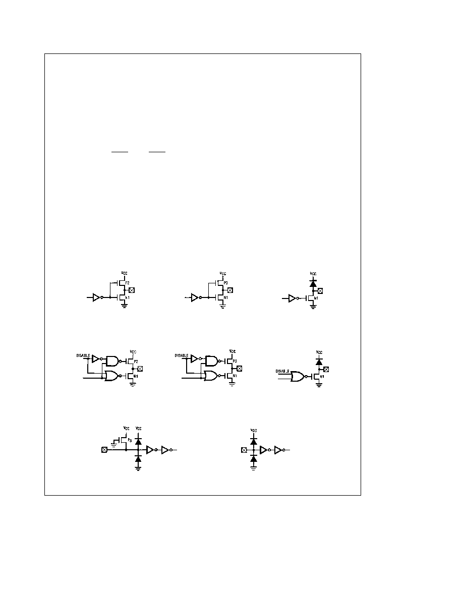
I O OPTIONS
Outputs have the following optional configurations illustrat-
ed in
Figure 11
a Standard
A CMOS push-pull buffer with an N-channel
device to ground in conjunction with a P-channel device
to V
CC
compatible with CMOS and LSTTL
b Low Current
This is the same configuration as a
above except that the sourcing current is much less
c Open Drain
An N-channel device to ground only allow-
ing external pull-up as required by the user's application
d Standard TRI-STATE L Output
A CMOS output buffer
similar to a which may be disabled by program control
e Low-Current TRI-STATE L Output
This is the same as
d above except that the sourcing current is much less
f Open-Drain TRI-STATE L Output
This has the N-chan-
nel device to ground only
All inputs have the following options
g Input with on chip load device to V
CC
h Hi-Z input which must be driven by the users logic
When using either the G or L I O ports as inputs a pull-up
device is necessary This can be an external device or the
following alternative is available Select the low-current out-
put option Now by setting the output registers to a logic
``1'' level the P-channel devices will act as the pull-up load
Note that when using the L ports in this fashion the Q regis-
ters must be set to a logic ``1'' level and the L drivers MUST
BE ENABLED by an LEI instruction (see description above)
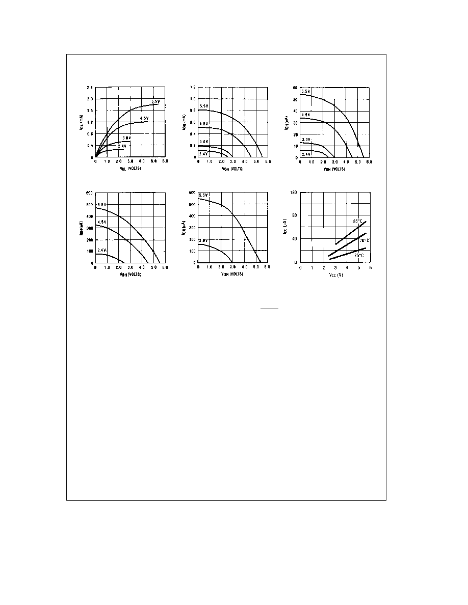
All output drivers use one or more of three common devices
numbered 1 to 3 Minimum and maximum current (I
OUT
and
V
OUT
) curves are given in
Figure 12 for each of these de-
vices to allow the designer to effectively use these I O con-
figurations
a Standard Push-Pull Output
b Low Current Push-Pull Output
c Open-Drain Output
d Standard TRI-STATE ``L'' Output
e Low Current TRI-STATE
``L'' Output
f Open Drain TRI-STATE
``L'' Output
TL DD 5259 � 14
g Input with Load
h Hi-Z Input
FIGURE 11 Input Output Configurations
18
Power Dissipation
(Continued)
Minimum Sink Current
Standard
Minimum Source Current
Low Current Option
Minimum Source Current
COP444C 424C 445C 425C
Low Current Option
Maximum Source Current
COP344C 345C 324C 325C
Low Current Option
Maximum Source Current
Maximum Quiescent Current
TL DD 5259 � 15
FIGURE 12 Input Output Characteristics
Option List
The
COP444C 445C 424C 425C COP426C
mask-pro-
grammable options are assigned numbers which corre-
spond with the COP444C 424C pins
The following is a list of options The options are pro-
grammed at the same time as the ROM pattern to provide
the user with the hardware flexibility to interface to various
I O components using little or no external circuitry
PLEASE FILL OUT THE OPTION TABLE on the next page
Xerox the option data and send it in with your disk or
EPROM
Option 1
e
0 Ground Pin
no options available
Option 2 CKO Pin
e
0 clock generator output to crystal resonator
e
1 HALT I O port
e
2 general purpose input with load device to V
CC
e
3 general purpose input high-Z
Option 3 CKI input
e
0 Crystal controlled oscillator input divide by 4
e
1 Crystal controlled oscillator input divide by 8
e
2 Crystal controlled oscillator input divide by 16
e
4 Single-pin RC controlled oscillator (divide by 4)
e
5 External oscillator input divide by 4
e
6 External oscillator input divide by 8
e
7 External oscillator input divide by 16
Option 4 RESET input
e
0 load device to V
CC
e
1 Hi-Z input
Option 5 L7 Driver
e
0 Standard TRI-STATE push-pull output
e
1 Low-current TRI-STATE push-pull output
e
2 Open-drain TRI-STATE output
Option 6 L6 Driver
(same as option 5)
Option 7 L5 Driver
(same as option 5)
Option 8 L4 Driver
(same as option 5)
Option 9 IN1 input
e
0 load device to V
CC
e
1 Hi-Z input
Option 10 IN2 input
(same as option 9)
Option 11
e
0 V
CC
Pin
no option available
Option 12 L3 Driver
(same as option 5)
Option 13 L2 Driver
(same as option 5)
Option 14 L1 Driver
(same as option 5)
Option 15 L0 Driver
(same as option 5)
Option 16 SI input
(same as option 9)
Option 17 SO Driver
e
0 Standard push-pull output
e
1 Low-current push-pull output
e
2 Open-drain output
19

Option List
(Continued)
Option 18 SK Driver
(same as option 17)
Option 19 IN0 Input
(same as option 9)
Option 20 IN3 Input
(same as option 9)
Option 21 G0 I O Port
(same as option 17)
Option 22 G1 I O Port
(same as option 17)
Option 23 G2 I O Port
(same as option 17)
Option 24 G3 I O Port
(same as option 17)
Option 25 D3 Output
(same as option 17)
Option 26 D2 Output
(same as option 17)
Option 27 D1 Output
(same as option 17)
Option 28 D0 Output
(same as option 17)
Option 29 Internal Initialization Logic
e
0 Normal operation
e
1 No internal initialization logic
Option 30 Dual Clock
e
0 Normal operation
e
1 Dual Clock D0 RC oscillator
e
2 Dual Clock D0 ext clock input
(
(opt
28 must
e
2)
Option 31 Timer
e
0 No Option Available
Option 32 Microbus
e
0 Normal
e
1 Microbus (opt
31 must
e
0)
Option 33 COP bonding
(1k and 2K Microcontroller)
e
0 28-pin package
e
1 24-pin package
e
2 Same die purchased in both
24 and 28 pin version
(1K Microcontroller only)
e
3 20-pin package
e
4 28- and 20-pin package
e
5 24- and 20-pin package
e
6 28- 24- and 20-pin package
Note
if opt
33
e
1 or 2 then opt
9 10 19 20 and 32
must
e
0
if opt
33
e
3 4 5 or 6 then opt
9 10 19
20 21 22 30 and 32 must
e
0
Option Table
The following option information is to be sent to National along with the EPROM
OPTION DATA
OPTION
1 VALUE
e
0
IS GROUND PIN
OPTION
2 VALUE
e
IS CKO PIN
OPTION
3 VALUE
e
IS CKI INPUT
OPTION
4 VALUE
e
IS RESET INPUT
OPTION
5 VALUE
e
IS L(7) DRIVER
OPTION
6 VALUE
e
IS L(6) DRIVER
OPTION
7 VALUE
e
IS L(5) DRIVER
OPTION
8 VALUE
e
IS L(4) DRIVER
OPTION
9 VALUE
e
IS IN1 INPUT
OPTION 10 VALUE
e
IS IN2 INPUT
OPTION 11 VALUE
e
IS VCC PIN
OPTION 12 VALUE
e
IS L(3) DRIVER
OPTION 13 VALUE
e
IS L(2) DRIVER
OPTION 14 VALUE
e
IS L(1) DRIVER
OPTION 15 VALUE
e
IS L(0) DRIVER
OPTION 16 VALUE
e
IS SI INPUT
OPTION DATA
OPTION 17 VALUE
e
IS SO DRIVER
OPTION 18 VALUE
e
IS SK DRIVER
OPTION 19 VALUE
e
IS IN0 INPUT
OPTION 20 VALUE
e
IS IN3 INPUT
OPTION 21 VALUE
e
IS G0 I O PORT
OPTION 22 VALUE
e
IS G1 I O PORT
OPTION 23 VALUE
e
IS G2 I O PORT
OPTION 24 VALUE
e
IS G3 I O PORT
OPTION 25 VALUE
e
IS D3 OUTPUT
OPTION 26 VALUE
e
IS D2 OUTPUT
OPTION 27 VALUE
e
IS D1 OUTPUT
OPTION 28 VALUE
e
IS D0 OUTPUT
OPTION 29 VALUE
e
IS INT INIT LOGIC
OPTION 30 VALUE
e
IS DUAL CLOCK
OPTION 31 VALUE
e
0
IS TIMER
OPTION 32 VALUE
e
IS MICROBUS
OPTION 33 VALUE
e
IS COP BONDING
20

21
Physical Dimensions
inches (millimeters)
20-Lead Hermetic Dual-In-Line Package (D)
Order Number COP326C-XXX D COP426C-XXX D
NS Package Number D20A
24-Lead Hermetic Dual-In-Line Package (D)
Order Number COP425C-XXX D COP325C-XXX D
COP445C-XXX D COP345C-XXX D
NS Package Number D24C
22
Physical Dimensions
inches (millimeters) (Continued)
28-Lead Hermetic Dual-In-Line Package (D)
Order Number COP424C-XXX D COP324C-XXX D
COP444C-XXX D COP344C-XXX D
NS Package Number D28C
20-Lead Molded Dual-In-Line Package (N)
Order Number COP426C-XXX N and COP326C-XXX N
NS Package Number N20A
23
COP424C
COP425C
COP426C
COP324C
COP325C
COP326C
and
COP444C
COP445C
COP344C
COP345C
Single-Chip
1k
and
2k
CMOS
Microcontrollers
Physical Dimensions
inches (millimeters) (Continued)
24-Lead Molded Dual-In-Line Package (N)
Order Number COP425C-XXX N COP325C-XXX N
COP445C-XXX N COP345C-XXX N
NS Package Number N24A
28-Lead Molded Dual-In-Line Package (N)
Order Number COP424C-XXX N COP324C-XXX N
COP444C-XXX N COP344C-XXX N
NS Package Number N28B
LIFE SUPPORT POLICY
NATIONAL'S PRODUCTS ARE NOT AUTHORIZED FOR USE AS CRITICAL COMPONENTS IN LIFE SUPPORT
DEVICES OR SYSTEMS WITHOUT THE EXPRESS WRITTEN APPROVAL OF THE PRESIDENT OF NATIONAL
SEMICONDUCTOR CORPORATION As used herein
1 Life support devices or systems are devices or
2 A critical component is any component of a life
systems which (a) are intended for surgical implant
support device or system whose failure to perform can
into the body or (b) support or sustain life and whose
be reasonably expected to cause the failure of the life
failure to perform when properly used in accordance
support device or system or to affect its safety or
with instructions for use provided in the labeling can
effectiveness
be reasonably expected to result in a significant injury
to the user
National Semiconductor
National Semiconductor
National Semiconductor
National Semiconductor
Corporation
Europe
Hong Kong Ltd
Japan Ltd
1111 West Bardin Road
Fax (a49) 0-180-530 85 86
13th Floor Straight Block
Tel 81-043-299-2309
Arlington TX 76017
Email cnjwge tevm2 nsc com
Ocean Centre 5 Canton Rd
Fax 81-043-299-2408
Tel 1(800) 272-9959
Deutsch Tel (a49) 0-180-530 85 85
Tsimshatsui Kowloon
Fax 1(800) 737-7018
English
Tel (a49) 0-180-532 78 32
Hong Kong
Fran ais Tel (a49) 0-180-532 93 58
Tel (852) 2737-1600
Italiano
Tel (a49) 0-180-534 16 80
Fax (852) 2736-9960
National does not assume any responsibility for use of any circuitry described no circuit patent licenses are implied and National reserves the right at any time without notice to change said circuitry and specifications