 | –≠–ª–µ–∫—Ç—Ä–æ–Ω–Ω—ã–π –∫–æ–º–ø–æ–Ω–µ–Ω—Ç: COP404CN | –°–∫–∞—á–∞—Ç—å:  PDF PDF  ZIP ZIP |
TL DD 5530
COP404C
ROMless
CMOS
Microcontrollers
April 1992
COP404C ROMless CMOS Microcontrollers
General Description
The COP404C ROMless Microcontroller is a member of the
COPS
TM
family fabricated using double-poly silicon gate
CMOS (microCMOS) technology The COP404C contains
CPU RAM I O and is identical to a COP444C device ex-
cept the ROM has been removed and pins have been add-
ed to output the ROM address and to input the ROM data
The COP404C can be configured by means of external
pins
to function as a COP444C
a COP424C
or a
COP410C Pins have been added to allow the user to select
the various functional options that are available on the fami-
ly of mask-programmed CMOS parts The COP404C is pri-
marily intended for use in the development and debug of a
COP program for the COP444C 445C COP424C 425C
and COP410C 411C devices prior to masking the final part
The COP404C is also appropriate in low volume applica-
tions or when the program might be changing
MICROBUS
TM
and MICROWIRE
TM
are trademarks of National Semiconductor Corporation
TRI-STATE
is a registered trademark of National Semiconductor Corporation
Features
Y
Accurate emulation of the COP444C COP424C and
COP410C
Y
Lowest Power Dissipation (50 mW typical)
Y
Fully static (can turn off the clock)
Y
Power saving IDLE state and HALT mode
Y
4 ms instruction time plus software selectable clocks
Y
128
c
4 RAM addresses 2k
c
8 ROM
Y
True vectored interrupt plus restart
Y
Three-level subroutine stack
Y
Single supply operation (2 4V to 5 5V)
Y
Programmable read write 8-bit timer event counter
Y
Internal binary counter register with MICROWIRE
TM
serial I O capability
Y
General purpose and TRI-STATE
outputs
Y
LSTTL CMOS compatible
Y
MICROBUS
TM
compatible
Y
Software hardware compatible with other members of
the COP400 family
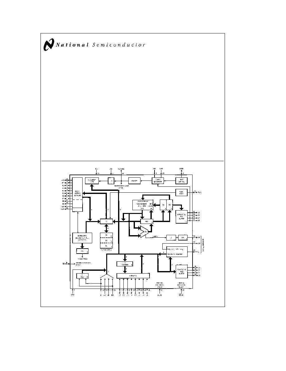
Block Diagram
TL DD 5530 ≠ 1
FIGURE 1 Block Diagram
C1995 National Semiconductor Corporation
RRD-B30M105 Printed in U S A
Absolute Maximum Ratings
Supply Voltage
6V
Voltage at any pin
b
0 3V to V
CC
a
0 3V
Total Allowable Source Current
25 mA
Total Allowable Sink Current
25 mA
Operating temperature range
0 to
a
70 C
Storage temperature range
b
65 C to
a
150 C
Lead temperature (soldering 10 sec )
300 C
DC Electrical Characteristics
0 C
s
T
a
s
70 C unless otherwise specified
Parameter
Conditions
Min
Max
Units
Operating Voltage
V
Power Supply Ripple
peak to peak
V
CC
V
Notes
Supply Current
V
CC
e
V t
c
e
m
s
m
A
Note
V
CC
e
V t
c
e
m
s
m
A
V
CC
e
V t
c
e
m
s
m
A
T
c
is instruction cycle time
HALT Mode Current
V
CC
e
V F
IN
e
kHz T
A
e
C
m
A
Note
V
CC
e
V F
IN
e
kHz T
A
e
C
m
A
Input Voltage Levels
RESET D
clock input
CKI
Logic High
V
CC
V
Logic Low
V
CC
V
All other inputs Note
Logic High
V
CC
V
Logic Low
V
CC
V
Input Pull up
current
V
CC
e
V V
IN
e
m
A
Hi Z input leakage
b
a
m
A
Input capacitance
pF
Note
Output Voltage Levels
Standard outputs
LSTTL Operation
V
CC
e
V
g
Logic High
I
OH
e b
m
A
V
Logic Low
I
OL
e
m
A
V
CMOS Operation
Logic High
I
OH
e b
m
A
V
CC
b
V
Logic Low
I
OL
e
m
A
V
Output current levels
Sink Note
V
CC
e
V V
OUT
e
V
CC
mA
V
CC
e
V V
OUT
e
V
CC
mA
Source Standard option
V
CC
e
V V
OUT
e
V
mA
V
CC
e
V V
OUT
e
V
mA
Source Low current option
V
CC
e
V V
OUT
e
V
m
A
V
CC
e
V V
OUT
e
V
m
A
Allowable Sink Source current per pin
mA
Note
Allowable Loading on CKOH
pF
Current needed to over ride HALT
Note
To continue
V
CC
e
V V
IN
e
V
CC
mA
To halt
V
CC
e
V V
IN
e
V
CC
mA
TRI STATE leakage current
b
a
m
A
Note
Absolute maximum ratings indicate limits beyond which damage to the device may occur DC and AC electrical specifications are not ensured when
operating the device at absolute maximum ratings
2
COP404C
AC Electrical Characteristics
0 C
s
T
A
s
70 C unless otherwise specified
Parameter
Conditions
Min
Max
Units
Instruction Cycle
V
CC
t
V
DC
m
s
Time t
c
V
l
V
CC
t
V
DC
m
s
Operating CKI
V
CC
t
V
DC
MHz
Frequency
V
l
V
CC
t
V
DC
kHz
Duty Cycle Note
f
e
MHz
Rise Time Note
f
e
MHz external clock
ns
Fall Time Note
ns
Instruction Cycle
R
e
k V
CC
e
V
Time using D as a
C
e
pF
m
s
RC Oscillator Dual
Clock Input Note
INPUTS See
Fig
t
SETUP
G Inputs
T
c
a
m
s
SI Input
V
CC
t
V
m
s
IP Input
m
s
All Others
*
m
s
t
HOLD
V
CC
t
V
m
s
V
l
V
CC
t
V
m
s
OUTPUT
PROPAGATION DELAY
V
OUT
e
V C
L
e
pF R
L
e
K
IP
IP
A
A
SKIP
t
PD
t
PD
V
CC
t
V
m
s
V
l
V
CC
t
V
m
s
AD DATA
t
PD
t
PD
V
CC
t
V
ns
V
l
V
CC
t
V
m
s
ALL OTHER OUTPUTS
t
PD
t
PD
V
CC
l
V
m
s
V
l
V
CC
t
V
m
s
MICROBUS TIMING
C
L
e
pF V
CC
e
V
g
Read Operation
Fig
Chip select stable before RD
b
t
CSR
ns
Chip select hold time for RD
b
t
RCS
ns
RD pulse width
b
t
RR
ns
Data delay from RD
b
t
RD
ns
RD to data floating
b
t
DF
Note
ns
Write Operation
Fig
Chip select stable before WR
b
t
CSW
ns
Chip select hold time for WR
b
t
WCS
ns
WR pulse width
b
t
WW
ns
Data set up time for WR
b
t
DW
ns
Data hold time for WR
b
t
WD
ns
INTR transition time from WR
b
t
WI
ns
Note 1
Supply current is measured after running for 2000 cycle times with a square-wave clock on CKI and all other pins pulled up to V
CC
with 20k resistors See
current drain equation on page 16
Note 2
Test conditions All inputs tied to V
CC
L lines in TRI-STATE mode and tied to Ground all outputs tied to Ground
Note 3
When forcing HALT current is only needed for a short time (approx 200 ns) to flip the HALT flip-flop
Note 4
This parameter is only sampled and not 100% tested Variation due to the device included
Note 5
Voltage change must be less than 0 1 V
CC
in a 1 ms period
Note 6
SO output sink current must be limited to keep V
OL
less than 0 2 V
CC
to prevent entering test mode
Note 7
MB TIN DUAL SEL10 SEL20 input levels at V
CC
or V
SS
3
Connection Diagram
Dual-In-Line Package
TL DD 5530 ≠ 2
Order Number COP404CN
See NS Package Number N48A
Pin Descriptions
Pin
Description
V
CC
Most positive voltage
V
SS
Ground
CKI
Clock input
RS
Reset input
CKOI
General purpose input
L
L
TRI STATE I O
G
G
general purpose I O
D
D
general purpose outputs
D
Either general purpose output
or Dual Clock RC input
IN
IN
general purpose inputs
SO
Serial data output
SI
Serial data input
SK
Serial data clock output
IP
IP
I O for ROM address and data
A
A
A
address outputs
SKIP
Skip status output
AD DATA
Clock output
MB
MICROBUS select input
CKOH
Halt I O pin
DUAL
Dual Clock select input
TIN
Timer input select pin should be
connected to GND
SEL
COP
C emulation select input
SEL
COP
C emulation select input
UNUSED
Ground
FIGURE 2
The internal architecture is shown in
Figure 1 Data paths
are illustrated in simplified form to depict how the various
logic elements communicate with each other in implement-
ing the instruction set of the device Positive logic is used
When a bit is set it is a logic ``1'' when a bit is reset it is a
logic ``0''
PROGRAM MEMORY
Program Memory consists of a 2048-byte external memory
(typically PROM) Words of this memory may be program
instructions constants or ROM addressing data
ROM addressing is accomplished by a 11-bit PC register
which selects one of the 8-bit words contained in ROM A
new address is loaded into the PC register during each in-
struction cycle Unless the instruction is a transfer of control
instruction the PC register is loaded with the next sequen-
tial 11-bit binary count value
Three levels of subroutine nesting are implemented by a
three level deep stack Each subroutine call or interrupt
pushes the next PC address into the stack Each return
pops the stack back into the PC register
DATA MEMORY
Data memory consists of a 512-bit RAM organized as 8
data registers of 16
c
4-bit digits RAM addressing is imple-
mented by a 7-bit B register whose upper 3 bits (B
r
) select 1
of 8 data registers and lower 4 bits (B
d
) select 1 of 16 4-bit
digits in the selected data register While the 4-bit contents
of the selected RAM digit (M) are usually loaded into or
from or exchanged with the A register (accumulator) it
may also be loaded into or from the Q latches or T counter
or loaded from the L ports RAM addressing may also be
performed directly by the LDD and XAD instructions based
upon the immediate operand field of these instructions The
B
d
register also serves as a source register for 4-bit data
sent directly to the D outputs
4
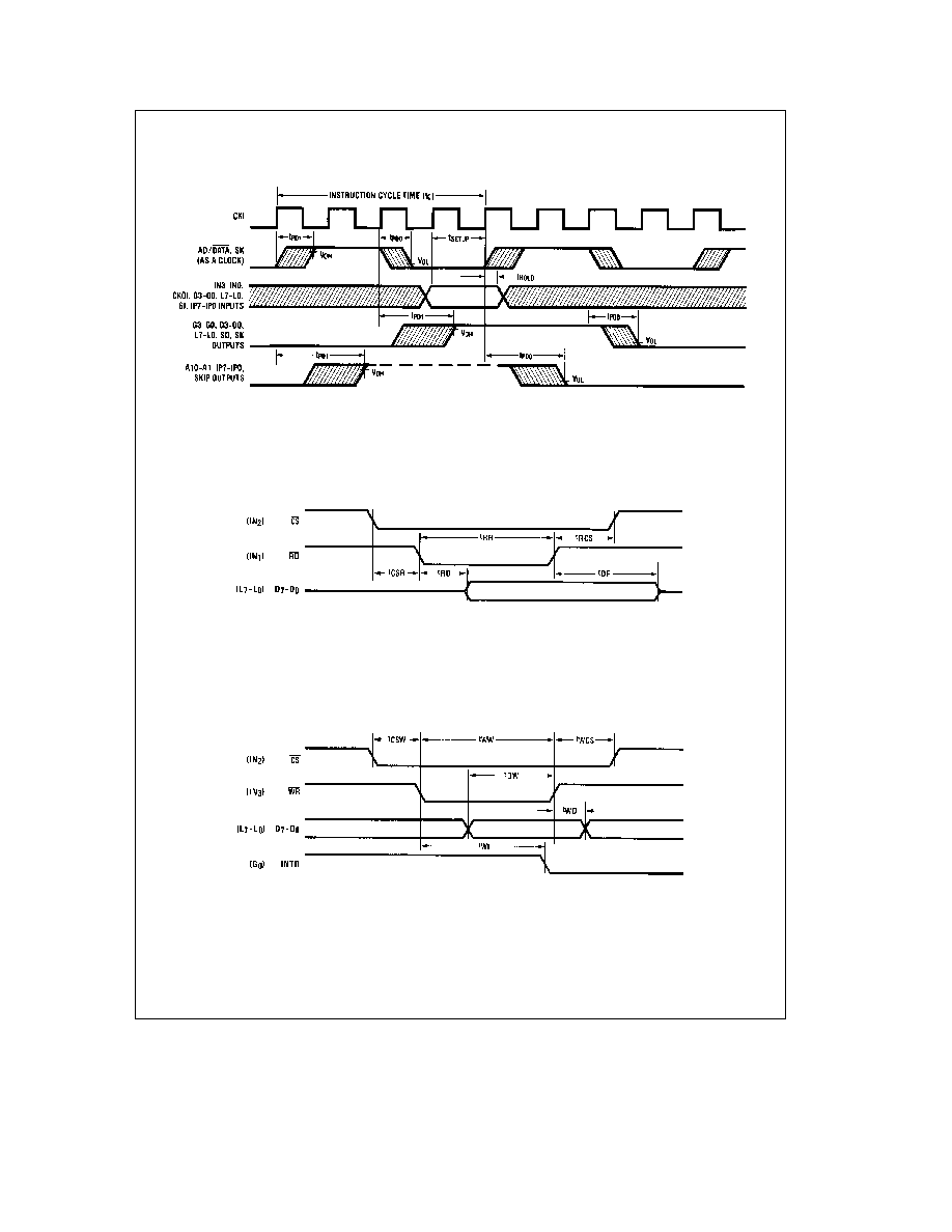
Timing Diagrams
TL DD 5530 ≠ 3
FIGURE 3 Input Output Timing
TL DD 5530 ≠ 4
FIGURE 4 MICROBUS Read Operation Timing
TL DD 5530 ≠ 5
FIGURE 5 MICROBUS Write Operation Timing
5