TL DD 5015
COP410CCOP411CCOP310CCOP311C
Single-Chip
CMOS
Microcontrollers
April 1992
COP410C COP411C COP310C COP311C
Single-Chip CMOS Microcontrollers
General Description
The COP410C COP411C COP310C and COP311C fully
static single-chip CMOS microcontrollers are members of
the COPS
TM
family fabricated using double-poly silicon-
gate CMOS technology These controller-oriented proces-
sors are complete microcomputers containing all system
timing internal logic ROM RAM and I O necessary to im-
plement dedicated control functions in a variety of applica-
tions Features include single supply operation a variety of
output configuration options with an instruction set internal
architecture and I O scheme designed to facilitate key-
board input display output and BCD data manipulation The
COP411C is identical to the COP410C but with 16 I O lines
instead of 20 They are an appropriate choice for use in
numerous human interface control environments Standard
test procedures and reliable high-density fabrication tech-
niques provide the medium to large volume customers with
a customized controller-oriented processor at a low end-
product cost
The COP310C COP311C is the extended temperature
range version of the COP410C COP411C
The COP404C should be used for exact emulation
Features
Y
Lowest power dissipation (40 mW typical)
Y
Low cost
Y
Power-saving HALT Mode with Continue function
Y
Powerful instruction set
Y
512 x 8 ROM 32 x 4 RAM
Y
20 I O lines (COP410C)
Y
Two-level subroutine stack
Y
DC to 4 ms instruction time
Y
Single supply operation (2 4V to 5 5V)
Y
General purpose and TRI-STATE
outputs
Y
Internal binary counter register with MICROWIRE
TM
compatible serial I O
Y
LSTTL CMOS compatible in and out
Y
Software hardware compatible with other members of
the COP400 family
Y
Extended temperature (
b
40 C to
a
85 C) devices
available
Y
The military temperature range devices (
b
55 C to
a
125 C) are specified on COP210C 211C data sheet
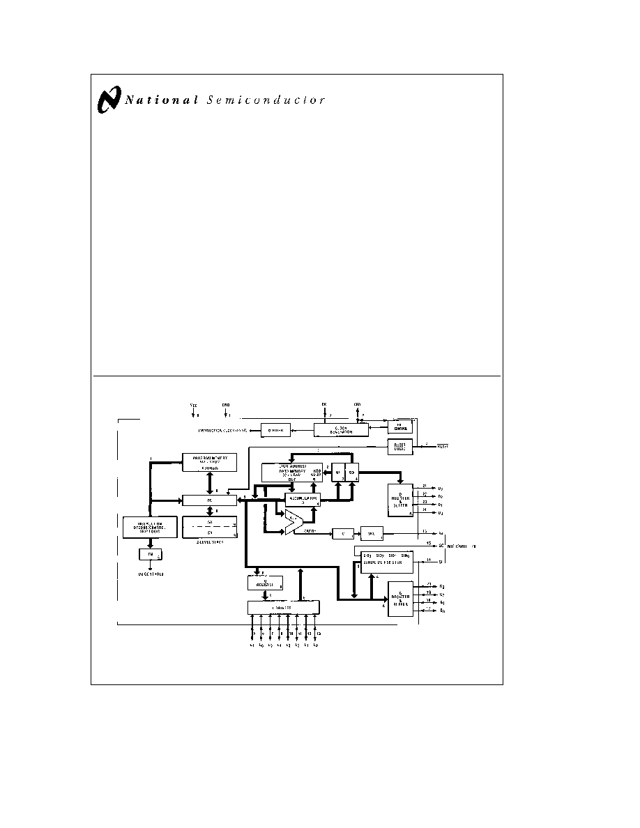
Block Diagram
TL DD 5015 � 1
FIGURE 1 COP410C
TRI-STATE
is a registered trademark of National Semiconductor Corporation
COPS
TM
and MICROWIRE
TM
are trademarks of National Semiconductor Corporation
C1995 National Semiconductor Corporation
RRD-B30M105 Printed in U S A
COP410C COP411C
Absolute Maximum Ratings
If Military Aerospace specified devices are required
please contact the National Semiconductor Sales
Office Distributors for availability and specifications
Supply Voltage
6V
Voltage at Any Pin
b
0 3V to V
CC
a
0 3V
Total Allowable Source Current
25 mA
Total Allowable Sink Current
25 mA
Operating Temperature Range
0 C to
a
70 C
Storage Temperature Range
b
65 C to
a
150 C
Lead Temperature (Soldering 10 sec )
300 C
Note
Absolute maximum ratings indicate limits beyond
which damage to the device may occur DC and AC electri-
cal specifications are not ensured when operating the de-
vice at absolute maximum ratings
DC Electrical Characteristics
0 C
s
T
A
s
70 C unless otherwise specified
Parameter
Conditions
Min
Max
Units
Operating Voltage
2 4
5 5
V
Power Supply Ripple (Notes 5 6)
0 1 V
CC
V
Supply Current (Note 1)
V
CC
e
2 4V t
c
e
125 ms
80
m
A
V
CC
e
5 0V t
c
e
16 ms
500
m
A
V
CC
e
5 0V t
c
e
4 ms
2000
m
A
(t
c
is instruction cycle time)
HALT Mode Current (Note 2)
V
CC
e
5 0V F
IN
e
0 kHz
30
m
A
V
CC
e
2 4V F
IN
e
0 kHz
10
m
A
Input Voltage Levels
RESET CKI
Logic High
0 9 V
CC
V
Logic Low
0 1 V
CC
V
All Other Inputs
Logic High
0 7 V
CC
V
Logic Low
0 2 V
CC
V
Hi-Z Input Leakage
b
1
a
1
m
A
Input Capacitance (Note 6)
7
pF
Output Voltage Levels
Standard Outputs
LSTTL Operation
V
CC
e
5 0V
g
10%
Logic High
I
OH
e b
25 mA
2 7
V
Logic Low
I
OL
e
400 mA
0 4
V
CMOS Operation
Logic High
I
OH
e b
10 mA
V
CC
b
0 2
V
Logic Low
I
OL
e
10 mA
0 2
V
Output Current Levels (Note 4)
(Except CKO)
Sink
V
CC
e
4 5V V
OUT
e
V
CC
1 2
mA
V
CC
e
2 4V V
OUT
e
V
CC
0 2
mA
Source (Standard
V
CC
e
4 5V V
OUT
e
0V
b
0 5
mA
Option)
V
CC
e
2 4V V
OUT
e
0V
b
0 1
mA
Source (Low
V
CC
e
4 5V V
OUT
e
0V
b
30
b
330
m
A
Current Option)
V
CC
e
2 4V V
OUT
e
0V
b
6
b
80
m
A
CKO Current Levels
(As Clock Out)
Sink
d
4
V
CC
e
4 5V CKI
e
V
CC
V
OUT
e
V
CC
0 3
mA
d
8
0 6
mA
d
16
1 2
mA
Source
d
4
V
CC
e
4 5V CKI
e
0V V
OUT
e
0V
b
0 3
mA
d
8
b
0 6
mA
d
16
b
1 2
mA
Allowable Sink Source
Current Per Pin (Note 4)
5
mA
2

COP410C COP411C
DC Electrical Characteristics
(Continued)
Parameter
Conditions
Min
Max
Units
Allowable Loading on CKO
(as HALT I O pin)
100
pF
Current Needed to
Override HALT
3
To Continue
V
CC
e
4 5V V
IN
e
0 2 V
CC
0 6
mA
To Halt
V
CC
e
4 5V V
IN
e
0 7 V
CC
1 6
mA
TRI-STATE or Open Drain
Leakage Current
b
2
a
2
m
A
Note 1
Supply current is measured after running for 2000 cycle times with a square-wave clock on CKI CKO open and all other pins pulled up to V
CC
with 5k
resistors See current drain equation on page 13
Note 2
The Halt mode will stop CKI from oscillating in the RC and crystal configurations
Note 3
When forcing HALT current is only needed for a short time (approximately 200 ns) to flip the HALT flip-flop
Note 4
SO output sink current must be limited to keep V
OL
less than 0 2 V
CC
when part is running in order to prevent entering test mode
Note 5
Voltage change must be less than 0 5V in a 1 ms period
Note 6
This parameter is only sampled and not 100% tested
Note 7
Variation due to the device included
COP410C COP411C
AC Electrical Characteristics
0 C
s
T
A
s
70 C unless otherwise specified
Parameter
Conditions
Min
Max
Units
Instruction Cycle Time (t
c
)
V
CC
t
4 5V
4
DC
m
s
4 5V
l
V
CC
t
2 4V
16
DC
m
s
Operating CKI
d
4 mode
DC
1 0
MHz
Frequency
d
8 mode
V
CC
t
4 5V
DC
2 0
MHz
d
16 mode
(
DC
4 0
MHz
d
4 mode
DC
250
kHz
d
8 mode
4 5V
l
V
CC
t
2 4V
DC
500
kHz
d
16 mode
(
DC
1 0
MHz
Instruction Cycle Time
R
e
30k
g
5% V
CC
e
5V
RC Oscillator
7
C
e
82 pF
g
5% (
d
4 Mode)
8
16
m
s
Duty Cycle
6
f
I
e
4 MHz
40
60
%
Rise Time
6
f
I
e
4 MHz External Clock
60
ns
Fall Time
6
f
I
e
4 MHz External Clock
40
ns
Inputs (See
Figure 3 )
t
SETUP
G Inputs
tc 4
a
0 7
m
s
SI Input
V
CC
t
4 5V
0 3
m
s
All Others
(
1 7
m
s
t
HOLD
V
CC
t
4 5V
0 25
m
s
V
CC
t
2 4V
1 0
m
s
Output Propagation
Delay
V
OUT
e
1 5V C
L
e
100 pF R
L
e
5k
t
PD1
t
PD0
V
CC
s
4 5V
1 0
m
s
t
PD1
t
PD0
V
CC
s
2 4V
4 0
m
s
3

COP310C COP311C
Absolute Maximum Ratings
If Military Aerospace specified devices are required
please contact the National Semiconductor Sales
Office Distributors for availability and specifications
Supply Voltage
6V
Voltage at Any Pin
b
0 3V to V
CC
a
0 3V
Total Allowable Source Current
25 mA
Total Allowable Sink Current
25 mA
Operating Temperature Range
b
40 C to
a
85 C
Storage Temperature Range
b
65 C to
a
150 C
Lead Temperature (Soldering 10 sec )
300 C
Note
Absolute maximum ratings indicate limits beyond
which damage to the device may occur DC and AC electri-
cal specifications are not ensured when operating the de-
vice at absolute maximum ratings
DC Electrical Characteristics
b
40 C
s
T
A
s
a
85 C unless otherwise specified
Parameter
Conditions
Min
Max
Units
Operating Voltage
3 0
5 5V
V
Power Supply Ripple (Notes 5 6)
0 1 V
CC
V
Supply Current (Note 1)
V
CC
e
3 0V t
c
e
125 ms
100
m
A
V
CC
e
5 0V t
c
e
16 ms
600
m
A
V
CC
e
5 0V t
c
e
4 ms
2500
m
A
(t
c
is instruction cycle time)
HALT Mode Current (Note 2)
V
CC
e
5 0V F
IN
e
0 kHz
50
m
A
V
CC
e
3 0V F
IN
e
0 kHz
20
m
A
Input Voltage Levels
RESET CKI
Logic High
0 9 V
CC
V
Logic Low
0 1 V
CC
V
All Other Inputs
Logic High
0 7 V
CC
V
Logic Low
0 2 V
CC
V
Hi-Z Input Leakage
b
2
a
2
m
A
Input Capacitance (Note 6)
7
pF
Output Voltage Levels
Standard Outputs
LSTTL Operation
V
CC
e
5 0V
g
10%
Logic High
I
OH
e b
25 mA
2 7
V
Logic Low
I
OL
e
400 mA
0 4
V
CMOS Operation
Logic High
I
OH
e b
10 mA
V
CC
b
0 2
V
Logic Low
I
OL
e
10 mA
0 2
V
Output Current Levels (Note 4)
(Except CKO)
Sink
V
CC
e
4 5V V
OUT
e
V
CC
1 2
mA
V
CC
e
3 0V V
OUT
e
V
CC
0 2
mA
Source (Standard
V
CC
e
4 5V V
OUT
e
0V
b
0 5
mA
Option)
V
CC
e
3 0V V
OUT
e
0V
b
0 1
mA
Source (Low
V
CC
e
4 5V V
OUT
e
0V
b
30
b
440
m
A
Current Option)
V
CC
e
3 0V V
OUT
e
0V
b
8
b
200
m
A
CKO Current Levels
(As Clock Out)
Sink
d
4
V
CC
e
4 5V CKI
e
V
CC
V
OUT
e
V
CC
0 3
mA
d
8
0 6
mA
d
16
1 2
mA
Source
d
4
V
CC
e
4 5V CKI
e
0V V
OUT
e
0V
b
0 3
mA
d
8
b
0 6
mA
d
16
b
1 2
mA
Allowable Sink Source
Current Per Pin (Note 4)
5
mA
4
COP310C COP311C
DC Electrical Characteristics
(Continued)
Parameter
Conditions
Min
Max
Units
Allowable Loading on CKO
(as HALT I O pin)
100
pF
Current Needed to
Override HALT
3
To Continue
V
CC
e
4 5V V
IN
e
0 2 V
CC
0 8
mA
To Halt
V
CC
e
4 5V V
IN
e
0 7 V
CC
2 0
mA
TRI-STATE or Open Drain
Leakage Current
b
4
a
4
m
A
Note 1
Supply current is measured after running for 2000 cycle times with a square-wave clock on CKI CKO open and all other pins pulled up to V
CC
with 5k
resistors See current drain equation on page 13
Note 2
The Halt mode will stop CKI from oscillating in the RC and crystal configurations
Note 3
When forcing HALT current is only needed for a short time (approximately 200 ns) to flip the HALT flip-flop
Note 4
SO output sink current must be limited to keep V
OL
less than 0 2 V
CC
when part is running in order to prevent entering test mode
Note 5
Voltage change must be less than 0 5V in a 1 ms period
Note 6
This parameter is only sampled and not 100% tested
Note 7
Variation due to the device included
COP310C COP311C
AC Electrical Characteristics
b
40 C
s
T
A
s
a
85 C unless otherwise specified
Parameter
Conditions
Min
Max
Units
Instruction Cycle Time (t
c
)
V
CC
t
4 5V
4
DC
m
s
4 5V
l
V
CC
t
3 0V
16
DC
m
s
Operating CKI
d
4 mode
DC
1 0
MHz
Frequency
d
8 mode
V
CC
t
4 5V
DC
2 0
MHz
d
16 mode
(
DC
4 0
MHz
d
4 mode
DC
250
kHz
d
8 mode
4 5V
l
V
CC
t
3 0V
DC
500
kHz
d
16 mode
(
DC
1 0
MHz
Instruction Cycle Time
R
e
30k
g
5% V
CC
e
5V
RC Oscillator
7
C
e
82 pF
g
5% (
d
4 Mode)
8
16
m
s
Duty Cycle
6
f
I
e
4 MHz
40
60
%
Rise Time
6
f
I
e
4 MHz External Clock
60
ns
Fall Time
6
f
I
e
4 MHz External Clock
40
ns
Inputs (See
Figure 3 )
t
SETUP
G Inputs
tc 4
a
0 7
m
s
SI Input
V
CC
t
4 5V
0 3
m
s
All Others
(
1 7
m
s
t
HOLD
V
CC
t
4 5V
0 25
m
s
V
CC
t
3 0V
1 0
m
s
Output Propagation
Delay
V
OUT
e
1 5V C
L
e
100 pF R
L
e
5k
t
PD1
t
PD0
V
CC
s
4 5V
1 0
m
s
t
PD1
t
PD0
V
CC
s
3 0V
4 0
m
s
5