 | –≠–ª–µ–∫—Ç—Ä–æ–Ω–Ω—ã–π –∫–æ–º–ø–æ–Ω–µ–Ω—Ç: COP472-3 | –°–∫–∞—á–∞—Ç—å:  PDF PDF  ZIP ZIP |
TL DD 6932
COP472-3
Liquid
Crystal
Display
Controller
July 1995
COP472-3 Liquid Crystal Display Controller
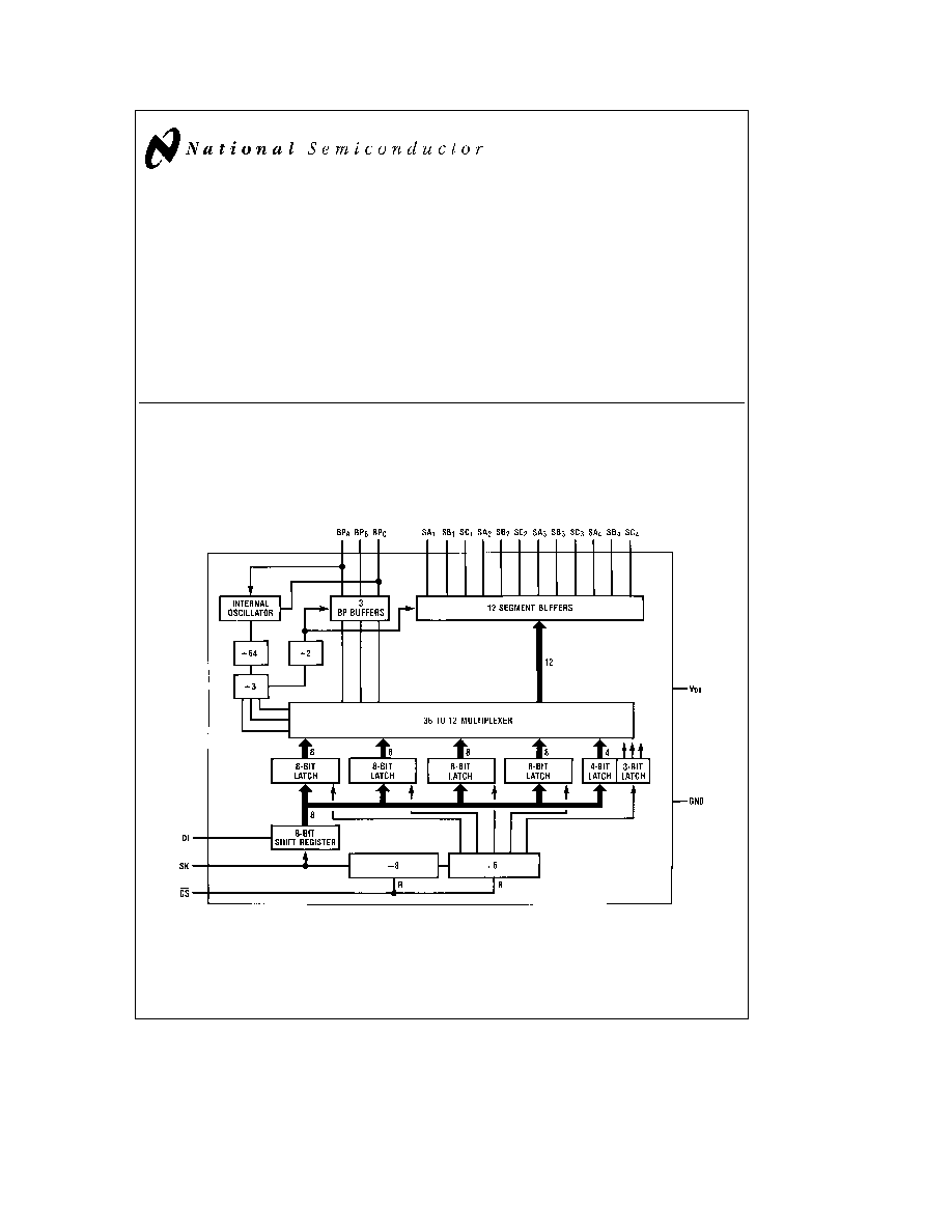
General Description
The COP472 ≠ 3 Liquid Crystal Display (LCD) Controller is a
peripheral member of the COPS
TM
family fabricated using
CMOS technology The COP472-3 drives a multiplexed liq-
uid crystal display directly Data is loaded serially and is held
in internal latches The COP472-3 contains an on-chip oscil-
lator and generates all the multi-level waveforms for back-
planes and segment outputs on a triplex display One
COP472-3 can drive 36 segments multiplexed as 3 x 12
(4
digit display) Two COP472-3 devices can be used to-
gether to drive 72 segments (3 x 24) which could be an 8
digit display
Features
Y
Direct interface to TRIPLEX LCD
Y
Low power dissipation (100 mW typ )
Y
Low cost
Y
Compatible with all COPS processors
Y
Needs no refresh from processor
Y
On-chip oscillator and latches
Y
Expandable to longer displays
Y
Operates from display voltage
Y
MICROWIRE
TM
compatible serial I O
Y
20-pin Dual-In-Line package and 20-pin SO
Block Diagram
TL DD 6932 ≠ 1
COPS
TM
and MICROWIRE
TM
are trademarks of National Semiconductor Corporation
C1996 National Semiconductor Corporation
RRD-B30M56 Printed in U S A
http
www national com
Absolute Maximum Ratings
Voltage at CS DI SK pins
b
0 3V to
a
9 5V
Voltage at all other Pins
b
0 3V to V
DD
a
0 3V
Operating Temperature Range
0 C to 70 C
Storage Temperature
b
65 C to
a
150 C
Lead Temp (Soldering 10 Seconds)
300 C
DC Electrical Characteristics
GND
e
0V V
DD
e
3 0V to 5 5V T
A
e
0 C to 70 C (depends on display characteristics)
Parameter
Conditions
Min
Max
Units
Power Supply Voltage V
DD
3 0
5 5
Volts
Power Supply Current I
DD
(Note 1)
V
DD
e
5 5V
250
m
A
V
DD
e
3V
100
m
A
Input Levels
DI SK CS
V
IL
0 8
Volts
V
IH
0 7 V
DD
9 5
Volts
BPA (as Osc in)
V
IL
0 6
Volts
V
IH
V
DD
b
0 6
V
DD
Volts
Output Levels BPC (as Osc Out)
V
OL
0 4
Volts
V
OH
V
DD
b
0 4
V
DD
Volts
Backplane Outputs (BPA BPB BPC)
V
BPA BPB BPC
ON
During
V
DD
b
D
V
V
DD
Volts
V
BPA BPB BPC
OFF
BP
a
Time
V
DD
b
D
V
V
DD
a
D
V
Volts
V
BPA BPB BPC
ON
During
0
D
V
Volts
V
BPA BPB BPC
OFF
BP
b
Time
V
DD
b
D
V
V
DD
a
D
V
Volts
Segment Outputs (SA
1
E
SA
4
)
V
SEG
ON
During
0
D
V
Volts
V
SEG
OFF
BP
a
Time
V
DD
b
D
V
V
DD
a
D
V
Volts
V
SEG
ON
During
V
DD
b
D
V
V
DD
Volts
V
SEG
OFF
BP
b
Time
V
DD
b
D
V
V
DD
a
D
V
Volts
Internal Oscillator Frequency
15
80
kHz
Frame Time (Int Osc
d
192)
2 4
12 8
ms
Scan Frequency (1 T
SCAN
)
39
208
Hz
SK Clock Frequency
4
250
kHz
SK Width
1 7
m
s
DI
Data Setup t
SETUP
1 0
m
s
Data Hold t
HOLD
100
ns
CS
t
SETUP
1 0
m
s
t
HOLD
1 0
m
s
Output Loading Capacitance
100
pF
Note 1
Power supply current is measured in stand-alone mode with all outputs open and all inputs at VDD
Note 2 D
V
e
0 05V
DD
http
www national com
2
Absolute Maximum Ratings
If Military Aerospace specified devices are required
please contact the National Semiconductor Sales
Office Distributors for availability and specifications
Voltage at CS DI SK Pins
b
0 3V to
a
9 5V
Voltage at All Other Pins
b
0 3V to V
DD
a
0 3V
Operating Temperature Range
b
40 C to
a
85 C
Storage Temperature
b
65 C to
a
150 C
Lead Temperature
(Soldering 10 seconds)
300 C
DC Electrical Characteristics
GND
e
0V V
DD
e
3 0V to 5 5V T
A
e b
40 C to
a
85 C (depends on display characteristics)
Parameter
Conditions
Min
Max
Units
Power Supply Voltage V
DD
3 0
5 5
Volts
Power Supply Current I
DD
(Note 1)
V
DD
e
5 5V
300
m
A
V
DD
e
3V
120
m
A
Input Levels
DI SK CS
V
IL
0 8
Volts
V
IH
0 7 V
DD
9 5
Volts
BPA (as Osc In)
V
IL
0 6
Volts
V
IH
V
DD
b
0 6
V
DD
Volts
Output Levels BPC (as Osc Out)
V
OL
0 4
Volts
V
OH
V
DD
b
0 4
V
DD
Volts
Backplane Outputs (BPA BPB BPC)
V
BPA BPB BPC
ON
During
V
DD
b
D
V
V
DD
Volts
V
BPA BPB BPC
OFF
BP
a
Time
V
DD
b
D
V
V
DD
a
D
V
Volts
V
BPA BPB BPC
ON
During
0
D
V
Volts
V
BPA BPB BPC
OFF
BP
b
Time
V
DD
b
D
V
V
DD
a
D
V
Volts
Segment Outputs (SA
1
E
SA
4
)
V
SEG
ON
During
0
D
V
Volts
V
SEG
OFF
BP
a
Time
V
DD
b
D
V
V
DD
a
D
V
Volts
V
SEG
ON
During
V
DD
b
D
V
V
DD
Volts
V
SEG
OFF
BP
b
Time
V
DD
b
D
V
V
DD
a
D
V
Volts
Internal Oscillator Frequency
15
80
kHz
Frame Time (Int Osc
d
192)
2 4
12 8
ms
Scan Frequency (1 T
SCAN
)
39
208
Hz
SK Clock Frequency
4
250
kHz
SK Width
1 7
m
s
DI
Data Setup t
SETUP
1 0
m
s
Data Hold t
HOLD
100
ns
CS
t
SETUP
1 0
m
s
t
HOLD
1 0
m
s
Output Loading Capacitance
100
pF
Note 1
Power supply current is measured in stand-alone mode with all outputs open and all inputs at V
DD
Note 2 D
V
e
0 05 V
DD
http
www national com
3
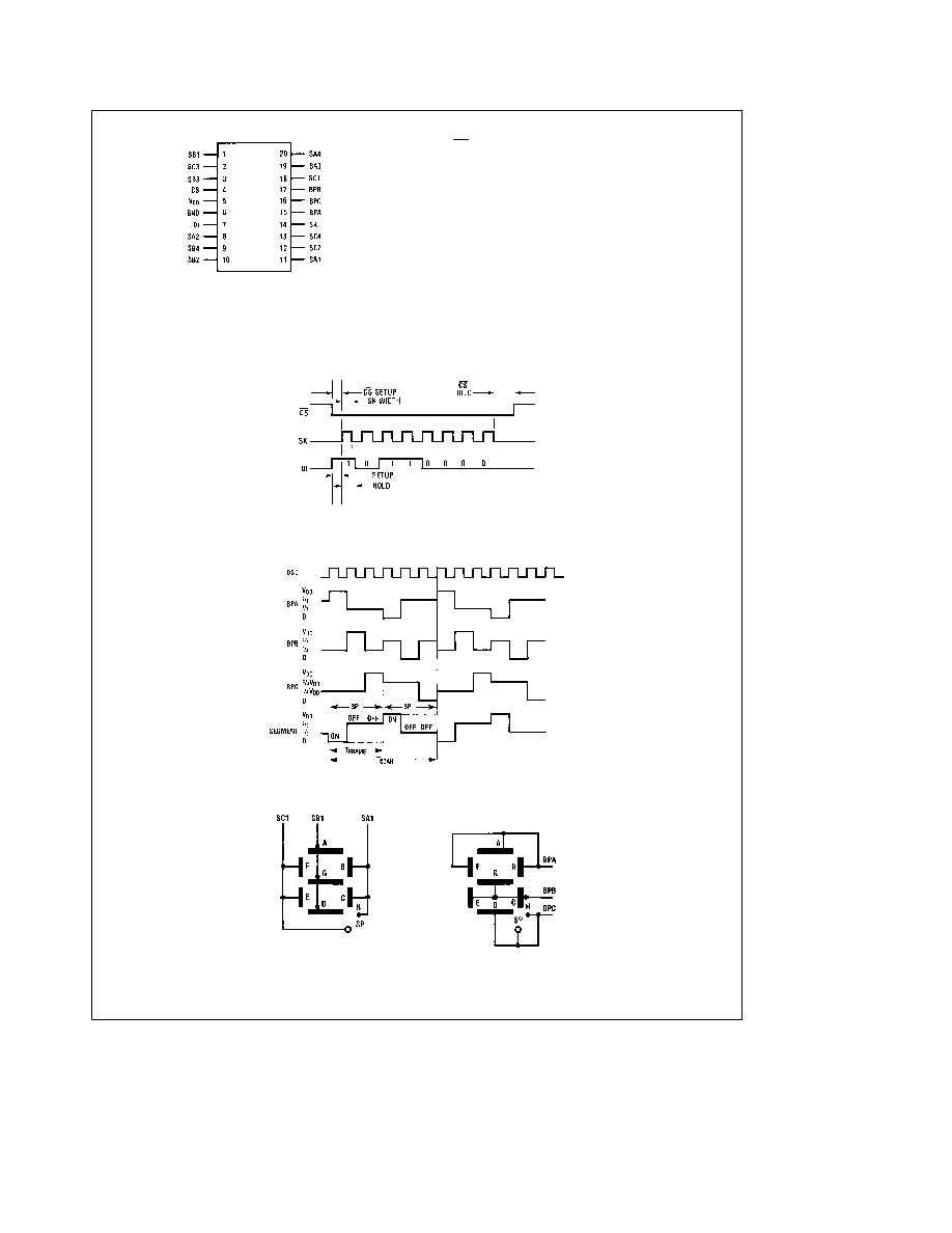
Dual-In-Line Package
TL DD 6932 ≠ 2
Top View
Order Number COP472MW-3 or COP472N-3
See NS Package Number M20A or N20A
Pin
Description
CS
Chip select
V
DD
Power supply (display voltage)
GND
Ground
DI
Serial data input
SK
Serial clock input
BP
A
Display backplane A (or oscillator in)
BP
B
Display backplane B
BP
C
Display backplane C (or oscillator out)
SA1ESC4
12 multiplexed outputs
FIGURE 2 Connection Diagram
TL DD 6932 ≠ 3
FIGURE 3 Serial Load Timing Diagram
TL DD 6932 ≠ 4
FIGURE 4 Backplane and Segment Waveforms
TL DD 6932 ≠ 5
FIGURE 5 Typical Display Internal Connections
Epson LD-370
http
www national com
4
Functional Description
The COP472-3 drives 36 bits of display information orga-
nized as twelve segments and three backplanes
The
COP472-3 requires 40 information bits 36 data and 4 con-
trol The function of each control bit is described below
Display information format is a function of the LCD intercon-
nections A typical segment backplane configuration is illus-
trated in
Figure 5 with this configuration the COP472-3 will
drive 4 digits of 9 segments
To adapt the COP472-3 to any LCD display configuration
the segment backplane multiplex scheme is illustrated in
Table I
Two or more COP472-3 chips can be cascaded to drive
additional segments There is no limit to the number of
COP472-3's that can be used as long as the output loading
capacitance does not exceed specification
TABLE I COP472-3 Segment Backplane
Multiplex Scheme
Bit Number
Segment
Data to
Backplane
Numeric Display
1
SA1 BPC
SH
2
SB1 BPB
SG
3
SC1 BPA
SF
4
SC1 BPB
SE
Digit 1
5
SB1 BPC
SD
6
SA1 BPB
SC
7
SA1 BPA
SB
8
SB1 BPA
SA
9
SA2 BPC
SH
10
SB2 BPB
SG
11
SC2 BPA
SF
12
SC2 BPB
SE
Digit 2
13
SB2 BPC
SD
14
SA2 BPB
SC
15
SA2 BPA
SB
16
SB2 BPA
SA
17
SA3 BPC
SH
18
SB3 BPB
SG
19
SC3 BPA
SF
20
SC3 BPB
SE
Digit 3
21
SB3 BPC
SD
22
SA3 BPB
SC
23
SA3 BPA
SB
24
SB3 BPA
SA
25
SA4 BPC
SH
26
SB4 BPB
SG
27
SC4 BPA
SF
28
SC4 BPB
SE
Digit 4
29
SB4 BPC
SD
30
SA4 BPB
SC
31
SA4 BPA
SB
32
SB4 BPA
SA
33
SC1 BPC
SPA
Digit 1
34
SC2 BPC
SP2
Digit 2
35
SC3 BPC
SP3
Digit 3
36
SC4 BPC
SP4
Digit 4
37
not used
38
Q6
39
Q7
40
SYNC
SEGMENT DATA BITS
Data is loaded in serially in sets of eight bits Each set of
segment data is in the following format
SA
SB
SC
SD
SE
SF
SG
SH
Data is shifted into an eight bit shift register The first bit of
the data is for segment H digit 1 The eighth bit is segment
A digit 1 A set of eight bits is shifted in and then loaded into
the digit one latches The second set of 8 bits is loaded into
digit two latches The third set into digit three latches and
the fourth set is loaded into digit four latches
CONTROL BITS
The fifth set of 8 data bits contains special segment data
and control data in the following format
SYNC
Q7
Q6
X
SP4
SP3
SP2
SP1
The first four bits shifted in contain the special character
segment data The fifth bit is not used The sixth and sev-
enth bits program the COP472-3 as a stand alone LCD driv-
er or as a master or slave for cascading COP472-3's BPC
of the master is connected to BPA of each slave The fol-
lowing table summarizes the function of bits six and seven
Q7
Q6
Function
BPC Output
BPA Output
1
1
Slave
Backplane
Oscillator
Output
Input
0
1
Stand Alone
Backplane
Backplane
Output
Output
1
0
Not Used
Internal
Oscillator
Osc Output
Input
0
0
Master
Internal
Backplane
Osc Output
Output
The eighth bit is used to synchronize two COP472-3's to
drive an 8
-digit display
http
www national com
5