 | –≠–ª–µ–∫—Ç—Ä–æ–Ω–Ω—ã–π –∫–æ–º–ø–æ–Ω–µ–Ω—Ç: COP620C | –°–∫–∞—á–∞—Ç—å:  PDF PDF  ZIP ZIP |
COP920C/COP922C/COP940C/COP942C
Absolute Maximum Ratings
(Note 1)
If Military/Aerospace specified devices are required,
please contact the National Semiconductor Sales Office/
Distributors for availability and specifications.
Supply Voltage (V
CC
)
7V
Voltage at any Pin
-0.3V to V
CC
+ 0.3V
Total Current into V
CC
Pin (Source)
50 mA
Total Current out of GND Pin (Sink)
60 mA
Storage Temperature Range
-65∞C to +140∞C
Note 1:
Absolute maximum ratings indicate limits beyond which damage to
the device may occur. DC and AC electrical specifications are not ensured
when operating the device at absolute maximum ratings.
DC Electrical Characteristics
COP92XC, COP94XC; 0∞C
T
A
+70∞C unless otherwise specified
Parameter
Condition
Min
Typ
Max
Units
Operating Voltage
COP9XXC
2.3
4.0
V
COP9XXCH
4.0
6.0
V
Power Supply Ripple (Note 2)
Peak to Peak
0.1 V
CC
V
Supply Current (Note 3)
CKI = 10 MHz
V
CC
= 6V, tc = 1 µs
6.0
mA
CKI = 4 MHz
V
CC
= 6V, tc = 2.5 µs
4.0
mA
CKI = 4 MHz
V
CC
= 4V, tc = 2.5 µs
2.0
mA
CKI = 1 MHz
V
CC
= 4V, tc = 10 µs
1.2
mA
HALT Current
V
CC
= 6V, CKI = 0 MHz
<
0.7
8.0
µA
(Note 4)
V
CC
= 4V, CKI = 0 MHz
<
0.4
5.0
µA
Input Levels
RESET , CKI
Logic High
0.9 V
CC
V
Logic Low
0.1 V
CC
V
All Other Inputs
Logic High
0.7 V
CC
V
Logic Low
0.2 V
CC
V
Hi-Z Input Leakage
V
CC
= 6.0V
-1
+1
µA
Input Pullup Current
V
CC
= 6.0V, V
IN
= 0V
-40
-250
µA
G Port Input Hysteresis
0.35 V
CC
V
Output Current Levels
D Outputs
Source
V
CC
= 4.5V, V
OH
= 3.8V
-0.4
mA
V
CC
= 2.3V, V
OH
= 1.6V
-0.2
mA
Sink
V
CC
= 4.5V, V
OL
= 1.0V
10
mA
V
CC
= 2.3V, V
OL
= 0.4V
2
mA
All Others
Source (Weak Pull-Up)
V
CC
= 4.5V, V
OH
= 3.2V
-10
-110
µA
V
CC
= 2.3V, V
OH
= 1.6V
-2.5
-33
µA
Source (Push-Pull Mode)
V
CC
= 4.5V, V
OH
= 3.8V
-0.4
mA
V
CC
= 2.3V, V
OH
= 1.6V
-0.2
Sink (Push-Pull Mode)
V
CC
= 4.5V, V
OL
= 0.4V
1.6
mA
V
CC
= 2.3V, V
OL
= 0.4V
0.7
TRI-STATE Leakage
V
CC
= 6.0V
-1.0
+1.0
µA
Allowable Sink/Source
Current Per Pin
D Outputs (Sink)
15
mA
All Others
3
mA
Maximum Input Current (Note 5)
Without Latchup (Room Temp)
Room Temp
±
100
mA
COP820C/COP840C
www.national.com
3
DC Electrical Characteristics
(Continued)
COP92XC, COP94XC; 0∞C
T
A
+70∞C unless otherwise specified
Parameter
Condition
Min
Typ
Max
Units
RAM Retention Voltage, Vr
500 ns Rise and Fall Time (Min)
2.0
V
Input Capacitance
7
pF
Load Capacitance on D2
1000
pF
Note 2: Rate of voltage change must be less than 0.5V/ms.
Note 3: Supply current is measured after running 2000 cycles with a square wave CKI input, CKO open, inputs at rails and outputs open.
Note 4: The HALT mode will stop CKI from oscillating in the RC and the Crystal configurations. Test conditions: All inputs tied to V
CC
, L and G0 -- G5 configured as
outputs and set high. The D port set to zero.
Note 5: Except pin G7: +100 mA, -25 mA (COP920C only). Sampled and not 100% tested. Pins G6 and RESET are designed with a high voltage input network for
factory testing. These pins allow input voltages greater than V
CC
and the pins will have sink current to V
CC
when biased at voltages greater than V
CC
(the pins do
not have source current when biased at a voltage below V
CC
). The effective resistance to V
CC
is 750
(typical). These two pins will not latch up. The voltage at the
pins must be limited to less than 14V.
AC Electrical Characteristics
0∞C
T
A
+70∞C unless otherwise specified
Parameter
Condition
Min
Typ
Max
Units
Instruction Cycle Time (tc)
Ext., Crystal/Resonator
V
CC
4.0V
1
DC
µs
(Div-by 10)
2.3V
V
CC
4.0V
2.5
DC
µs
R/C Oscillator Mode
V
CC
4.0V
3
DC
µs
(Div-by 10)
2.3V
V
CC
4.0V
7.5
DC
µs
CKI Clock Duty Cycle (Note 6)
fr = Max
40
60
%
Rise Time (Note 6)
fr = 10 MHz Ext Clock
12
ns
Fall Time (Note 6)
fr = 10 MHz Ext Clock
8
ns
Inputs
t
SETUP
V
CC
4.0V
200
ns
2.3V
V
CC
4.0V
500
ns
t
HOLD
V
CC
4.0V
60
ns
2.3V
V
CC
4.0V
150
ns
Output Propagation Delay
C
L
= 100 pF, R
L
= 2.2 k
t
PD1
, t
PD0
SO, SK
V
CC
4.0V
0.7
µs
2.5V
V
CC
4.0V
1.75
µs
All Others
V
CC
4.0V
1
µs
2.5V
V
CC
4.0V
2.5
µs
MICROWIRE
TM
Setup Time (t
UWS
)
20
ns
MICROWIRE Hold Time (t
UWH
)
56
ns
MICROWIRE Output Propagation
Delay (t
UPD
)
220
ns
Input Pulse Width
Interrupt Input High Time
t
C
Interrupt Input Low Time
t
C
Timer Input High Time
t
C
Timer Input Low Time
t
C
Reset Pulse Width
1.0
µs
Note 6: Parameter sampled (not 100% tested).
COP820C/COP840C
www.national.com
4
COP820C/COP822C/COP840C/COP842C
Absolute Maximum Ratings
(Note 7)
If Military/Aerospace specified devices are required,
please contact the National Semiconductor Sales Office/
Distributors for availability and specifications.
Supply Voltage (V
CC
)
7V
Voltage at any Pin
-0.3V to V
CC
+ 0.3V
Total Current into V
CC
Pin (Source)
50 mA
Total Current out of GND Pin (Sink)
60 mA
Storage Temperature Range
-65∞C to +140∞C
Note 7:
Absolute maximum ratings indicate limits beyond which damage to
the device may occur. DC and AC electrical specifications are not ensured
when operating the device at absolute maximum ratings.
DC Electrical Characteristics
COP82XC, COP84XC; -40∞C
T
A
+85∞C unless otherwise specified
Parameter
Condition
Min
Typ
Max
Units
Operating Voltage
2.5
6.0
V
Power Supply Ripple (Note 8)
Peak to Peak
0.1 V
CC
V
Supply Current (Note 9)
CKI = 10 MHz
V
CC
= 6V, tc = 1 µs
6.0
mA
CKI = 4 MHz
V
CC
= 6V, tc = 2.5 µs
4.0
mA
CKI = 4 MHz
V
CC
= 4.0V, tc = 2.5 µs
2.0
mA
CKI = 1 MHz
V
CC
= 4.0V, tc = 10 µs
1.2
mA
HALT Current (Note 10)
V
CC
= 6V, CKI = 0 MHz
<
1
10
µA
Input Levels
RESET , CKI
Logic High
0.9 V
CC
V
Logic Low
0.1 V
CC
V
All Other Inputs
Logic High
0.7 V
CC
V
Logic Low
0.2 V
CC
V
Hi-Z Input Leakage
V
CC
= 6.0V
-2
+2
µA
Input Pullup Current
V
CC
= 6.0V, V
IN
= 0V
-40
-250
µA
G Port Input Hysteresis
0.35 V
CC
V
Output Current Levels
D Outputs
Source
V
CC
= 4.5V, V
OH
= 3.8V
-0.4
mA
V
CC
= 2.5V, V
OH
= 1.8V
-0.2
mA
Sink
V
CC
= 4.5V, V
OL
= 1.0V
10
mA
V
CC
= 2.5V, V
OL
= 0.4V
2
mA
All Others
Source (Weak Pull-Up)
V
CC
= 4.5V, V
OH
= 3.2V
-10
-110
µA
V
CC
= 2.5V, V
OH
= 1.8V
-2.5
-33
µA
Source (Push-Pull Mode)
V
CC
= 4.5V, V
OH
= 3.8V
-0.4
mA
V
CC
= 2.5V, V
OH
= 1.8V
-0.2
Sink (Push-Pull Mode)
V
CC
= 4.5V, V
OL
= 0.4V
1.6
mA
V
CC
= 2.5V, V
OL
= 0.4V
0.7
TRI-STATE Leakage
-2.0
+2.0
µA
Allowable Sink/Source
Current Per Pin
D Outputs (Sink)
15
mA
All Others
3
mA
Maximum Input Current (Note 11)
Without Latchup (Room Temp)
Room Temp
±
100
mA
RAM Retention Voltage, Vr
500 ns Rise and Fall Time
(Min)
2.0
V
Input Capacitance
7
pF
COP820C/COP840C
www.national.com
5
DC Electrical Characteristics
(Continued)
COP82XC, COP84XC; -40∞C
T
A
+85∞C unless otherwise specified
Parameter
Condition
Min
Typ
Max
Units
Load Capacitance on D2
1000
pF
Note 8: Rate of voltage change must be less than 0.5V/ms.
Note 9: Supply current is measured after running 2000 cycles with a square wave CKI input, CKO open, inputs at rails and outputs open.
Note 10: The HALT mode will stop CKI from oscillating in the RC and the Crystal configurations. Test conditions: All inputs tied to V
CC
, L and G0 -- G5 configured
as outputs and set high. The D port set to zero.
Note 11: Except pin G7: +100 mA, -25 mA (COP820C only). Sampled and not 100% tested. Pins G6 and RESET are designed with a high voltage input network
for factory testing. These pins allow input voltages greater than V
CC
and the pins will have sink current to V
CC
when biased at voltages greater than V
CC
(the pins
do not have source current when biased at a voltage below V
CC
). The effective resistance to V
CC
is 750
(typical). These two pins will not latch up. The voltage at
the pins must be limited to less than 14V.
AC Electrical Characteristics
-40∞C
T
A
+85∞C unless otherwise specified
Parameter
Condition
Min
Typ
Max
Units
Instruction Cycle Time (tc)
Ext. or Crystal/Resonator
V
CC
4.5V
1
DC
µs
(Div-by 10)
2.5V
V
CC
<
4.5V
2.5
DC
µs
R/C Oscillator Mode
V
CC
4.5V
3
DC
µs
(Div-by 10)
2.5V
V
CC
<
4.5V
7.5
DC
µs
CKI Clock Duty Cycle (Note 12)
fr = Max
40
60
%
Rise Time (Note 12)
fr = 10 MHz Ext Clock
12
ns
Fall Time (Note 12)
fr = 10 MHz Ext Clock
8
ns
Inputs
t
SETUP
V
CC
4.5V
200
ns
2.5V
V
CC
<
4.5V
500
ns
t
HOLD
V
CC
4.5V
60
ns
2.5V
V
CC
<
4.5V
150
ns
Output Propagation Delay
C
L
= 100 pF, R
L
= 2.2 k
t
PD1
, t
PD0
SO, SK
V
CC
4.5V
0.7
µs
2.5V
V
CC
<
4.5V
1.75
µs
All Others
V
CC
4.5V
1
µs
2.5V
V
CC
<
4.5V
2.5
µs
MICROWIRE Setup Time (t
UWS
)
20
ns
MICROWIRE Hold Time (t
UWH
)
56
ns
MICROWIRE Output Propagation
Delay (t
UPD
)
220
ns
Input Pulse Width
Interrupt Input High Time
t
C
Interrupt Input Low Time
t
C
Timer Input High Time
t
C
Timer Input Low Time
t
C
Reset Pulse Width
1.0
µs
Note 12: Parameter sampled (not 100% tested).
COP820C/COP840C
www.national.com
6
Timing Diagram
DS009103-19
FIGURE 2. MICROWIRE/PLUS Timing
COP820C/COP840C
www.national.com
7
COP620C/COP622C/COP640C/COP642C
Absolute Maximum Ratings
(Note 13)
If Military/Aerospace specified devices are required,
please contact the National Semiconductor Sales Office/
Distributors for availability and specifications.
Supply Voltage (V
CC
)
6V
Voltage at any Pin
-0.3V to V
CC
+ 0.3V
Total Current into V
CC
Pin (Source)
40 mA
Total Current out of GND Pin (Sink)
48 mA
Storage Temperature Range
-65∞C to +140∞C
Note 13:
Absolute maximum ratings indicate limits beyond which damage to
the device may occur. DC and AC electrical specifications are not ensured
when operating the device at absolute maximum ratings.
DC Electrical Characteristics
COP62XC, COP64XC; -55∞C
T
A
+125∞C unless otherwise specified
Parameter
Condition
Min
Typ
Max
Units
Operating Voltage
4.5
5.5
V
Power Supply Ripple (Note 14)
Peak to Peak
0.1 V
CC
V
Supply Current (Note 15)
CKI = 10 MHz
V
CC
= 5.5V, tc = 1 µs
6.0
mA
CKI = 4 MHz
V
CC
= 5.5V, tc = 2.5 µs
4
mA
HALT Current (Note 16)
V
CC
= 5.5V, CKI = 0 MHz
<
10
30
µA
Input Levels
RESET , CKI
Logic High
0.9 V
CC
V
Logic Low
0.1 V
CC
V
All Other Inputs
Logic High
0.7 V
CC
V
Logic Low
0.2 V
CC
V
Hi-Z Input Leakage
V
CC
= 5.5V
-5
+5
µA
Input Pullup Current
V
CC
= 4.5V, V
IN
= 0V
-35
-300
µA
G Port Input Hysteresis
0.35 V
CC
V
Output Current Levels
D Outputs
Source
V
CC
= 4.5V, V
OH
= 3.8V
-0.35
mA
Sink
V
CC
= 4.5V, V
OL
= 1.0V
9
mA
All Others
Source (Weak Pull-Up)
V
CC
= 4.5V, V
OH
= 3.2V
-9
-120
µA
Source (Push-Pull Mode)
V
CC
= 4.5V, V
OH
= 3.8V
-0.35
mA
Sink (Push-Pull Mode)
V
CC
= 4.5V, V
OL
= 0.4V
1.4
mA
TRI-STATE Leakage
-5.0
+5.0
µA
Allowable Sink/Source
Current Per Pin
D Outputs (Sink)
12
mA
All Others
2.5
mA
Maximum Input Current (Room Temp)
Without Latchup (Note 18)
Room Temp
±
100
mA
RAM Retention Voltage, Vr
500 ns Rise and Fall Time
(Min)
2.5
V
Input Capacitance
7
pF
Load Capacitance on D2
1000
pF
Note 14: Rate of voltage change must be less than 0.5V/ms.
Note 15: Supply current is measured after running 2000 cycles with a square wave CKI input, CKO open, inputs at rails and outputs open.
Note 16: The HALT mode will stop CKI from oscillating in the RC and the Crystal configurations. Test conditions: All inputs tied to V
CC
, L and G0 -- G5 configured
as outputs and set high. The D port set to zero.
Note 17: Except pin G7: +100 mA, -25 mA (COP620C only). Sampled and not 100% tested. Pins G6 and RESET are designed with a high voltage input network
for factory testing. These pins allow input voltages greater than V
CC
and the pins will have sink current to V
CC
when biased at voltages greater than V
CC
(the pins
do not have source current when biased at a voltage below V
CC
). The effective resistance to V
CC
is 750
(typical). These two pins will not latch up. The voltage at
the pins must be limited to less than 14V.
COP820C/COP840C
www.national.com
8
AC Electrical Characteristics
-55∞C
T
A
+125∞C unless otherwise specified
Parameter
Condition
Min
Typ
Max
Units
Instruction Cycle Time (tc)
Ext. or Crystal/Resonant
V
CC
4.5V
1
DC
µs
(Div-by 10)
CKI Clock Duty Cycle (Note 18)
fr = Max
40
60
%
Rise Time (Note 18)
fr = 10 MHz Ext Clock
12
ns
Fall Time (Note 18)
fr = 10 MHz Ext Clock
8
ns
Inputs
t
SETUP
V
CC
4.5V
220
ns
t
HOLD
V
CC
4.5V
66
ns
Output Propagation Delay
R
L
= 2.2k, C
L
= 100 pF
t
PD1
, t
PD0
SO, SK
V
CC
4.5V
0.8
µs
All Others
V
CC
4.5V
1.1
µs
MICROWIRE Setup Time (t
UWS
)
20
ns
MICROWIRE Hold Time (t
UWH
)
56
ns
MICROWIRE Output Valid Time
(t
UPD
)
220
ns
Input Pulse Width
Interrupt Input High Time
t
C
Interrupt Input Low Time
t
C
Timer Input High Time
t
C
Timer Input Low Time
t
C
Reset Pulse Width
1
µs
Note 18: Parameter sampled (not 100% tested).
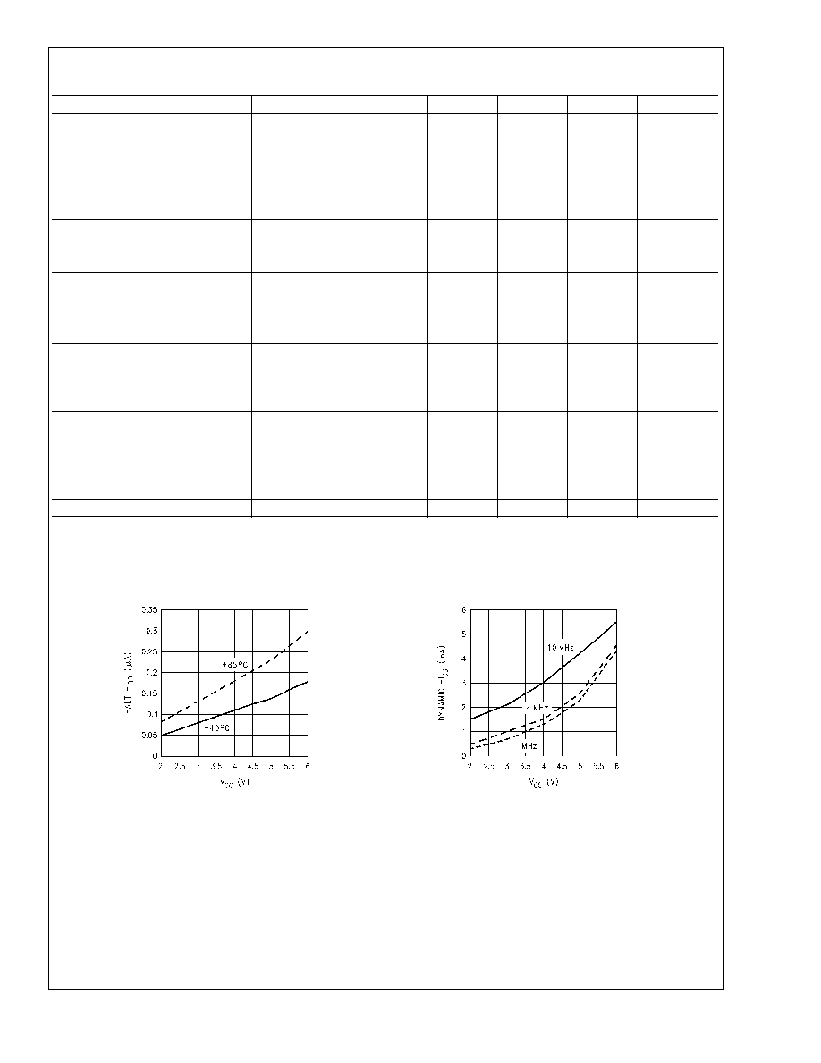
Typical Performance Characteristics
(-40∞C
T
A
+85∞C)
Halt -- I
DD
DS009103-20
Dynamic -- I
DD
(Crystal Clock Option)
DS009103-21
COP820C/COP840C
www.national.com
9
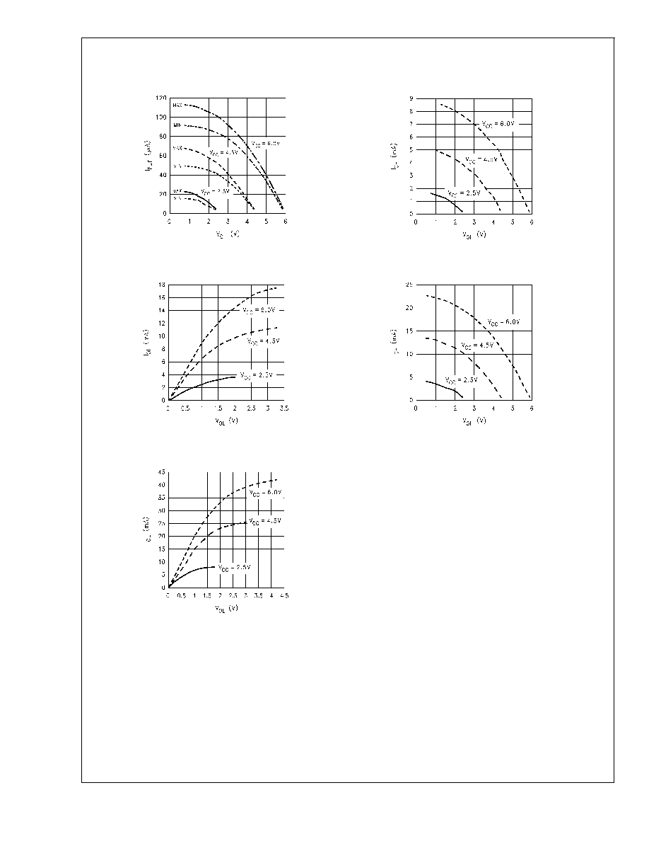
Typical Performance Characteristics
(-40∞C
T
A
+85∞C) (Continued)
Port L/G Weak Pull-Up Source Current
DS009103-22
Port L/G Push-Pull Source Current
DS009103-23
Port L/G Push-Pull Sink Current
DS009103-24
Port D Source Current
DS009103-25
Port D Sink Current
DS009103-26
COP820C/COP840C
www.national.com
10
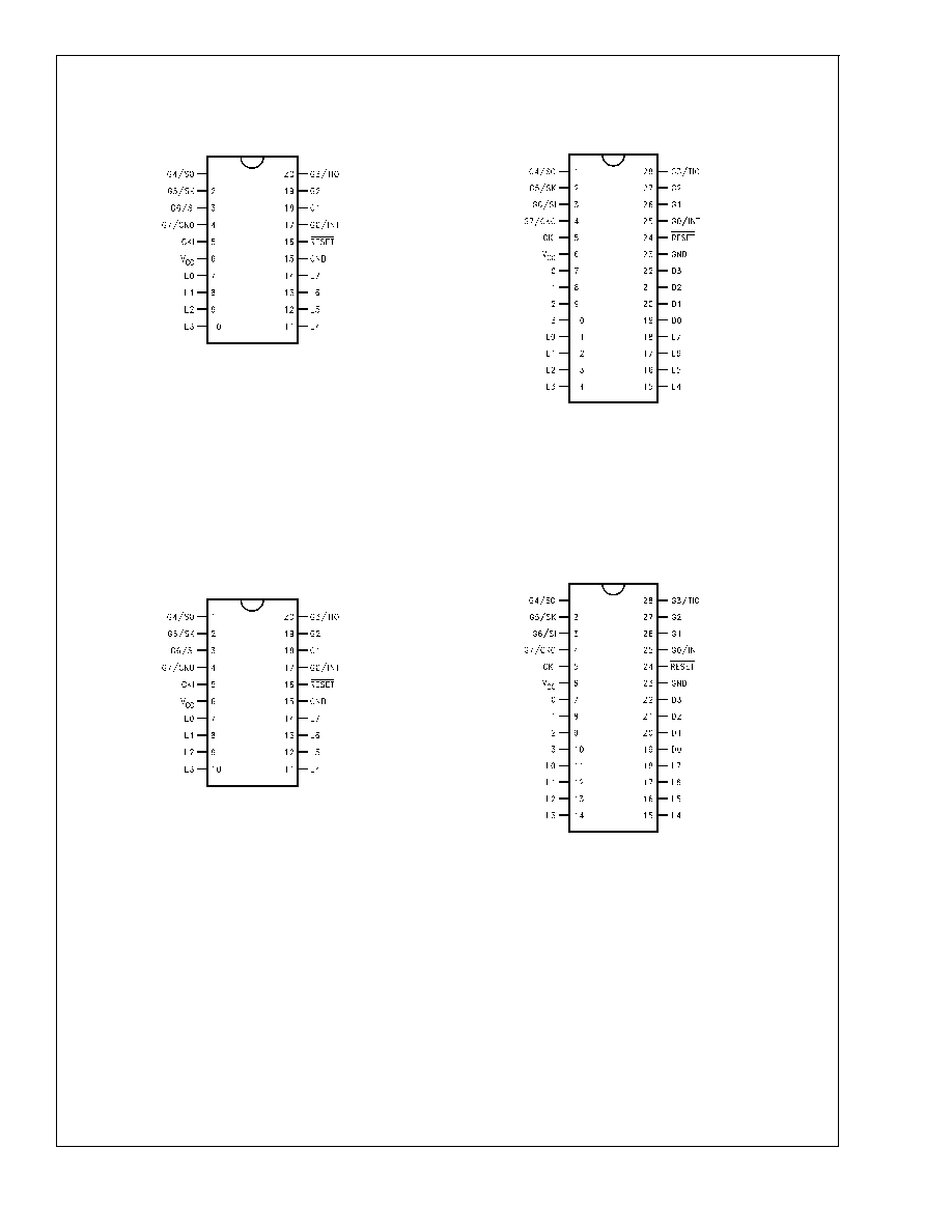
Connection Diagrams
DUAL-IN-LINE PACKAGE
20 DIP
DS009103-3
Top View
Order Number COP622C-XXX/N,
COP642C-XXX/N, COP822C-XXX/N,
COP842C-XXX/N, COP922C-XXX/N,
COP942C-XXX/N, COP922CH-XXX/N or
COP942CH-XXX/N
See NS Package Number N20A
28 DIP
DS009103-5
Order Number COP620C-XXX/N,
COP640C-XXX/N, COP820C-XXX/N,
COP840C-XXX/D,COP920C-XXX/N,
COP940C-XXX/N,
COP920CH-XXX/N or
COP940CH-XXX/N
See NS Package Number N28B
SURFACE MOUNT
20 SO Wide
DS009103-2
Top View
Order Number COP822C-XXX/WM,
COP842C-XXX/WM, COP922C-XXX/WM,
COP942C-XXX/WM,
COP922CH-XXX/WM or
COP942CH-XXX/WM
See NS Package Number M20B
28-Lead SO
DS009103-18
Order Number COP820C-XXX/WM,
COP840C-XXX/WM,
COP920C-XXX/WM,
COP940C-XXX/WM,
COP920CH-XXX/WM or
COP940CH-XXX/WM
See NS Package Number M28B
COP820C/COP840C
www.national.com
11
Connection Diagrams
(Continued)
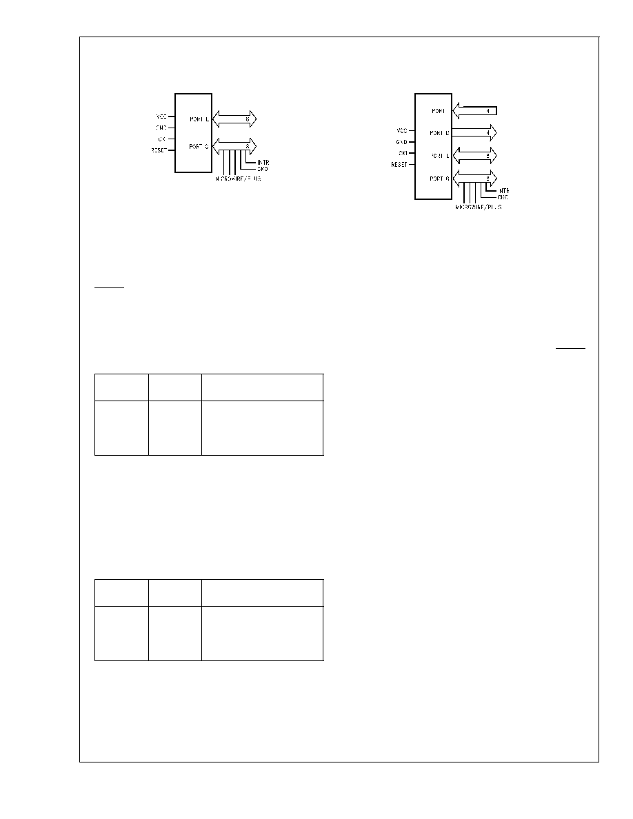
Pin Descriptions
V
CC
and GND are the power supply pins.
CKI is the clock input. This can come from an external
source, a R/C generated oscillator or a crystal (in conjunc-
tion with CKO). See Oscillator description.
RESET is the master reset input. See Reset description.
PORT I is a four bit Hi-Z input port.
PORT L is an 8-bit I/O port.
There are two registers associated with each L I/O port: a
data register and a configuration register. Therefore, each L
I/O bit can be individually configured under software control
as shown below:
Port L
Config.
Port L
Data
Port L
Setup
0
0
Hi-Z Input (TRI-STATE)
0
1
Input With Weak Pull-Up
1
0
Push-Pull "0" Output
1
1
Push-Pull "1" Output
Three data memory address locations are allocated for
these ports, one for data register, one for configuration reg-
ister and one for the input pins.
PORT G is an 8-bit port with 6 I/O pins (G0≠G5) and 2 input
pins (G6, G7). All eight G-pins have Schmitt Triggers on the
inputs. The G7 pin functions as an input pin under normal
operation and as the continue pin to exit the HALT mode.
There are two registers with each I/O port: a data register
and a configuration register. Therefore, each I/O bit can be
individually configured under software control as shown be-
low.
Port G
Config.
Port G
Data
Port G
Setup
0
0
Hi-Z Input (TRI-STATE)
0
1
Input With Weak Pull-Up
1
0
Push-Pull "0" Output
1
1
Push-Pull "1" Output
Three data memory address locations are allocated for
these ports, one for data register, one for configuration reg-
ister and one for the input pins. Since G6 and G7 are input
only pins, any attempt by the user to set them up as outputs
by writing a one to the configuration register will be disre-
garded. Reading the G6 and G7 configuration bits will return
zeros. Note that the chip will be placed in the HALT mode by
setting the G7 data bit.
Six bits of Port G have alternate features:
G0
INTR (an external interrupt)
G3
TIO (timer/counter input/output)
G4
SO (MICROWIRE serial data output)
G5
SK (MICROWIRE clock I/O)
G6
SI (MICROWIRE serial data input)
G7
CKO crystal oscillator output (selected by mask option)
or HALT restart input (general purpose input)
Pins G1 and G2 currently do not have any alternate func-
tions.
PORT D is a four bit output port that is set high when RESET
goes low. Care must be exercised with the D2 pin operation.
At RESET, the external load on this pin must ensure that the
output voltage stays above 0.9 V
CC
to prevent the device
from entering special modes. Also, keep the external loading
on the D2 pin to less than 1000 pf.
Functional Description
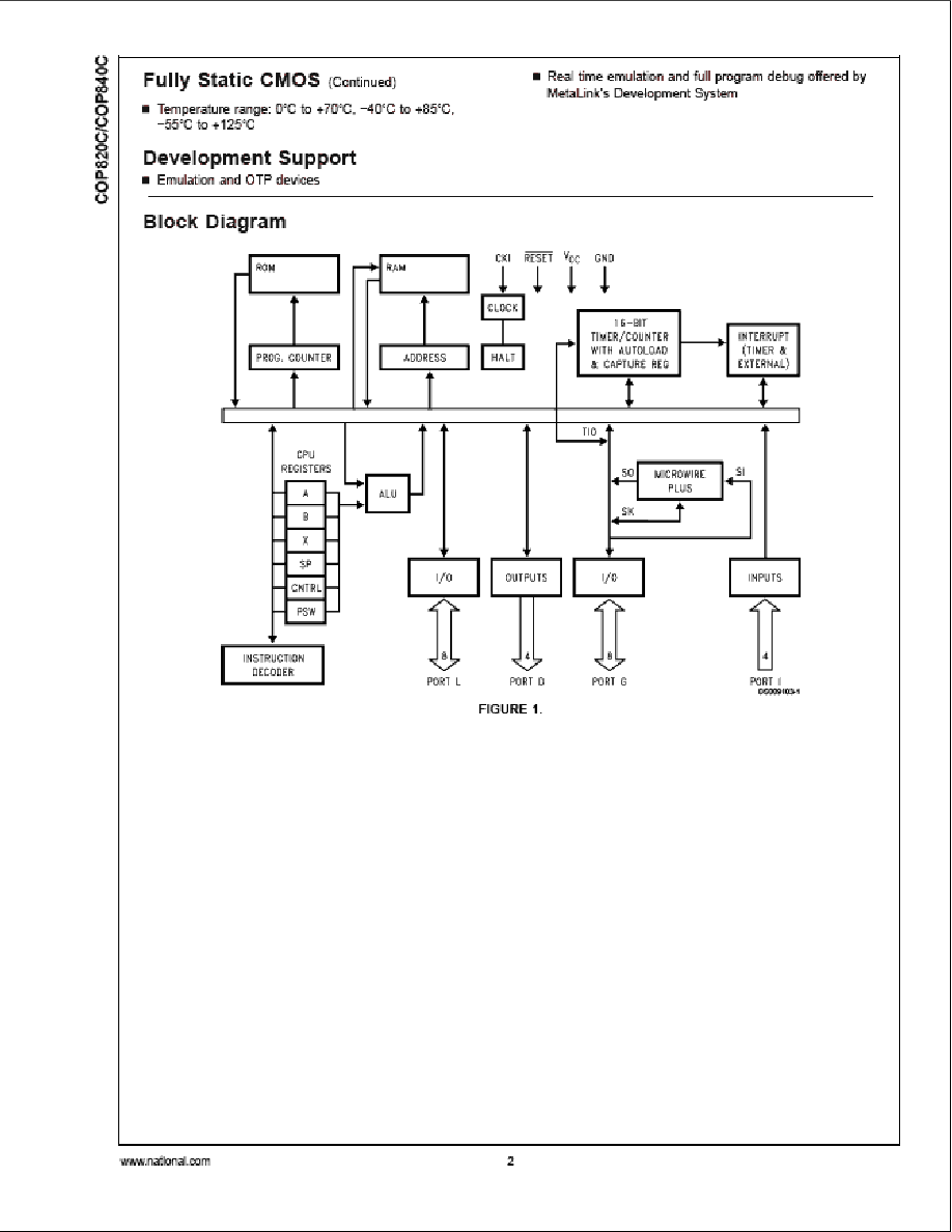
Figure 1 shows the block diagram of the internal architec-
ture. Data paths are illustrated in simplified form to depict
how the various logic elements communicate with each
other in implementing the instruction set of the device.
ALU AND CPU REGISTERS
The ALU can do an 8-bit addition, subtraction, logical or shift
operation in one cycle time.
There are five CPU registers:
A is the 8-bit Accumulator register
PU is the upper 7 bits of the program counter (PC)
PL is the lower 8 bits of the program counter (PC)
B is the 8-bit address register, can be auto incremented or
decremented.
X is the 8-bit alternate address register, can be incremented
or decremented.
SP is the 8-bit stack pointer, points to subroutine stack (in
RAM).
B, X and SP registers are mapped into the on chip RAM. The
B and X registers are used to address the on chip RAM. The
SP register is used to address the stack in RAM during sub-
routine calls and returns.
PROGRAM MEMORY
Program memory for the COP820C family consists of 1024
bytes of ROM (2048 bytes of ROM for the COP840C family).
These bytes may hold program instructions or constant data.
20 DIP/SO
DS009103-6
28 DIP/SO
DS009103-8
COP820C/COP840C
www.national.com
12
Functional Description
(Continued)
The program memory is addressed by the 15-bit program
counter (PC). ROM can be indirectly read by the LAID in-
struction for table lookup.
DATA MEMORY
The data memory address space includes on chip RAM, I/O
and registers. Data memory is addressed directly by the in-
struction or indirectly by the B, X and SP registers.
The COP820C family has 64 bytes of RAM and the
COP840C family has 128 bytes of RAM. Sixteen bytes of
RAM are mapped as "registers" that can be loaded immedi-
ately, decremented or tested. Three specific registers: B, X
and SP are mapped into this space, the other bytes are
available for general usage.
The instruction set permits any bit in memory to be set, reset
or tested. All I/O and registers (except the A & PC) are
memory mapped; therefore, I/O bits and register bits can be
directly and individually set, reset and tested.
Note: RAM contents are undefined upon power-up.
RESET
The RESET input when pulled low initializes the microcon-
troller. Initialization will occur whenever the RESET input is
pulled low. Upon initialization, the ports L and G are placed in
the TRI-STATE mode and the Port D is set high. The PC,
PSW and CNTRL registers are cleared. The data and con-
figuration registers for Ports L & G are cleared.
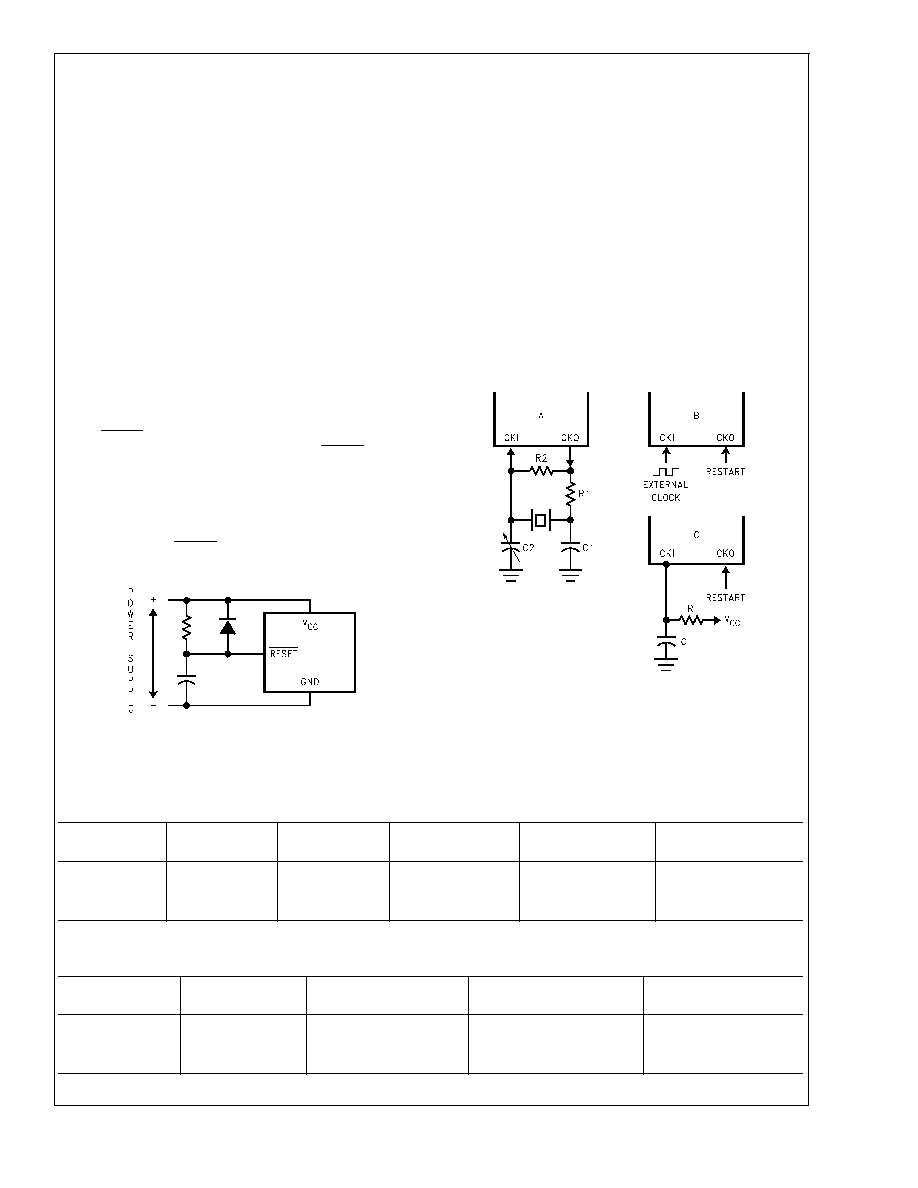
The external RC network shown in
Figure 3 should be used
to ensure that the RESET pin is held low until the power sup-
ply to the chip stabilizes.
OSCILLATOR CIRCUITS
Figure 4 shows the three clock oscillator configurations.
A. CRYSTAL OSCILLATOR
The device can be driven by a crystal clock. The crystal net-
work is connected between the pins CKI and CKO.
Table 1 shows the component values required for various
standard crystal values.
B. EXTERNAL OSCILLATOR
CKI can be driven by an external clock signal. CKO is avail-
able as a general purpose input and/or HALT restart control.
C. R/C OSCILLATOR
CKI is configured as a single pin RC controlled Schmitt trig-
ger oscillator. CKO is available as a general purpose input
and/or HALT restart control.
Table 2I shows the variation in the oscillator frequencies as
functions of the component (R and C) values.
OSCILLATOR MASK OPTIONS
The device can be driven by clock inputs between DC and
10 MHz.
TABLE 1. Crystal Oscillator Configuration, T
A
= 25∞C
R1
(k
)
R2
(M
)
C1
(pF)
C2
(pF)
CKI Freq
(MHz)
Conditions
0
1
30
30≠36
10
V
CC
= 5V
0
1
30
30≠36
4
V
CC
= 5V
0
1
200
100≠150
0.455
V
CC
= 5V
TABLE 2. RC Oscillator Configuration, T
A
= 25∞C
R
(k
)
C
(pF)
CKI Freq.
(MHz)
Instr. Cycle
(µs)
Conditions
3.3
82
2.2 to 2.7
3.7 to 4.6
V
CC
= 5V
5.6
100
1.1 to 1.3
7.4 to 9.0
V
CC
= 5V
6.8
100
0.9 to 1.1
8.8 to 10.8
V
CC
= 5V
Note 19: 3k
R
200k, 50 pF
C
200 pF
DS009103-9
RC
5X Power Supply Rise Time
FIGURE 3. Recommended Reset Circuit
DS009103-10
FIGURE 4. Crystal and R-C Connection Diagrams
COP820C/COP840C
www.national.com
13
Functional Description
(Continued)
The device has three mask options for configuring the clock
input. The CKI and CKO pins are automatically configured
upon selecting a particular option.
∑
Crystal (CKI/10) CKO for crystal configuration
∑
External (CKI/10) CKO available as G7 input
∑
R/C (CKI/10) CKO available as G7 input
G7 can be used either as a general purpose input or as a
control input to continue from the HALT mode.
HALT MODE
The device supports a power saving mode of operation:
HALT. The controller is placed in the HALT mode by setting
the G7 data bit, alternatively the user can stop the clock in-
put. In the HALT mode all internal processor activities includ-
ing the clock oscillator are stopped. The fully static architec-
ture freezes the state of the controller and retains all
information until continuing. In the HALT mode, power re-
quirements are minimal as it draws only leakage currents
and output current. The applied voltage (V
CC
) may be de-
creased down to Vr (minimum RAM retention voltage) with-
out altering the state of the machine.
There are two ways to exit the HALT mode: via the RESET
or by the CKO pin. A low on the RESET line reinitializes the
microcontroller and starts executing from the address
0000H. A low to high transition on the CKO pin (only if the ex-
ternal or the R/C clock option is selected) causes the micro-
controller to continue with no reinitialization from the address
following the HALT instruction. This also resets the G7 data
bit.
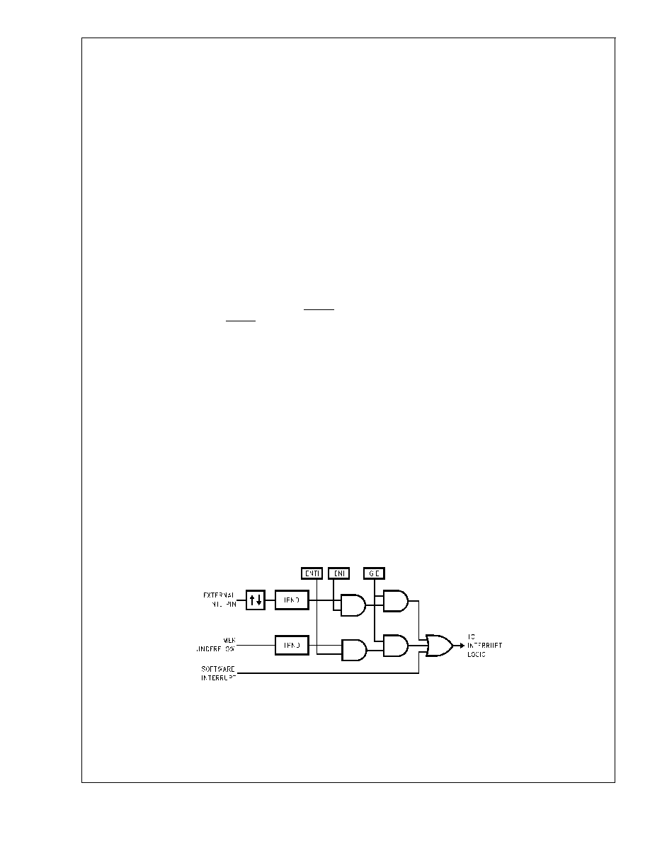
INTERRUPTS
There are three interrupt sources, as shown below.
A maskable interrupt on external G0 input (positive or nega-
tive edge sensitive under software control)
A maskable interrupt on timer underflow or timer capture
A non-maskable software/error interrupt on opcode zero
INTERRUPT CONTROL
The GIE (global interrupt enable) bit enables the interrupt
function. This is used in conjunction with ENI and ENTI to se-
lect one or both of the interrupt sources. This bit is reset
when interrupt is acknowledged.
ENI and ENTI bits select external and timer interrupt respec-
tively. Thus the user can select either or both sources to in-
terrupt the microcontroller when GIE is enabled.
IEDG selects the external interrupt edge (0 = rising edge, 1
= falling edge). The user can get an interrupt on both rising
and falling edges by toggling the state of IEDG bit after each
interrupt.
IPND and TPND bits signal which interrupt is pending. After
interrupt is acknowledged, the user can check these two bits
to determine which interrupt is pending. This permits the in-
terrupts to be prioritized under software. The pending flags
have to be cleared by the user. Setting the GIE bit high in-
side the interrupt subroutine allows nested interrupts.
The software interrupt does not reset the GIE bit. This
means that the controller can be interrupted by other inter-
rupt sources while servicing the software interrupt.
INTERRUPT PROCESSING
The interrupt, once acknowledged, pushes the program
counter (PC) onto the stack and the stack pointer (SP) is
decremented twice. The Global Interrupt Enable (GIE) bit is
reset to disable further interrupts. The microcontroller then
vectors to the address 00FFH and resumes execution from
that address. This process takes 7 cycles to complete. At the
end of the interrupt subroutine, any of the following three in-
structions return the processor back to the main program:
RET, RETSK or RETI. Either one of the three instructions will
pop the stack into the program counter (PC). The stack
pointer is then incremented twice. The RETI instruction addi-
tionally sets the GIE bit to re-enable further interrupts.
Any of the three instructions can be used to return from a
hardware interrupt subroutine. The RETSK instruction
should be used when returning from a software interrupt
subroutine to avoid entering an infinite loop.
Note: There is always the possibility of an interrupt occurring during an in-
struction which is attempting to reset the GIE bit or any other interrupt
enable bit. If this occurs when a single cycle instruction is being used
to reset the interrupt enable bit, the interrupt enable bit will be reset but
an interrupt may still occur. This is because interrupt processing is
started at the same time as the interrupt bit is being reset. To avoid this
scenario, the user should always use a two, three, or four cycle instruc-
tion to reset interrupt enable bits.
DS009103-11
FIGURE 5. Interrupt Block Diagram
COP820C/COP840C
www.national.com
14
Functional Description
(Continued)
DETECTION OF ILLEGAL CONDITIONS
The device contains a hardware mechanism that allows it to
detect illegal conditions which may occur from coding errors,
noise and `brown out' voltage drop situations. Specifically it
detects cases of executing out of undefined ROM area and
unbalanced stack situations.
Reading an undefined ROM location returns 00 (hexadeci-
mal) as its contents. The opcode for a software interrupt is
also '00'. Thus a program accessing undefined ROM will
cause a software interrupt.
Reading an undefined RAM location returns an FF (hexa-
decimal). The subroutine stack grows down for each subrou-
tine call. By initializing the stack pointer to the top of RAM,
the first unbalanced return instruction will cause the stack
pointer to address undefined RAM. As a result the program
will attempt to execute from FFFF (hexadecimal), which is an
undefined ROM location and will trigger a software interrupt.
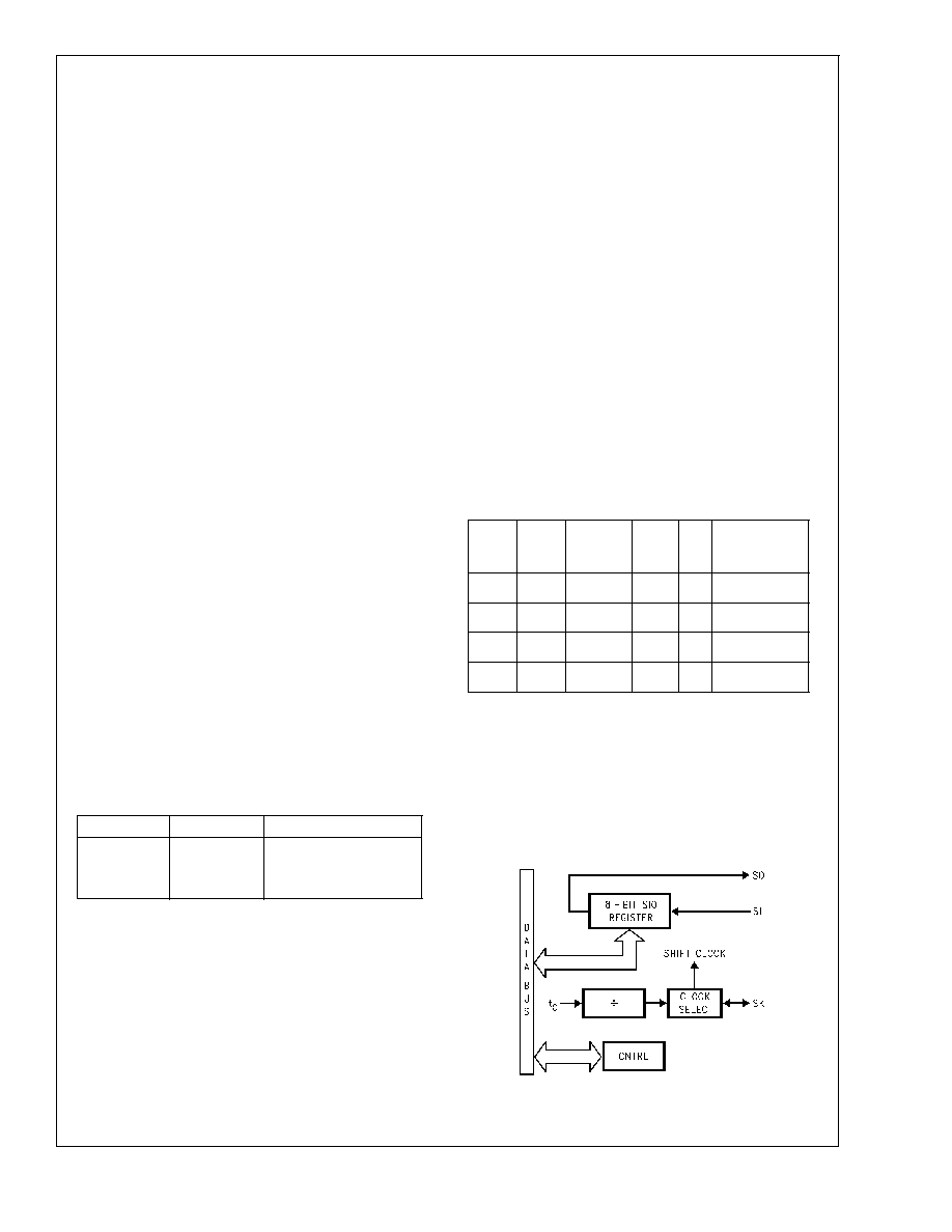
MICROWIRE/PLUS
TM
MICROWIRE/PLUS is a serial synchronous bidirectional
communications interface. The MICROWIRE/PLUS capabil-
ity enables the device to interface with any of National Semi-
conductor's MICROWIRE peripherals (i.e. A/D converters,
display drivers, EEPROMS, etc.) and with other microcon-
trollers which support the MICROWIRE/PLUS interface. It
consists of an 8-bit serial shift register (SIO) with serial data
input (SI), serial data output (SO) and serial shift clock (SK).
Figure 6 shows the block diagram of the MICROWIRE/PLUS
interface.
The shift clock can be selected from either an internal source
or an external source. Operating the MICROWIRE/PLUS in-
terface with the internal clock source is called the Master
mode of operation. Similarly, operating the MICROWIRE/
PLUS interface with an external shift clock is called the Slave
mode of operation.
The CNTRL register is used to configure and control the
MICROWIRE/PLUS mode. To use the MICROWIRE/PLUS,
the MSEL bit in the CNTRL register is set to one. The SK
clock rate is selected by the two bits, SL0 and SL1, in the
CNTRL register.
Table 3I details the different clock rates that
may be selected.
TABLE 3.
SL1
SL0
SK Cycle Time
0
0
2t
C
0
1
4t
C
1
x
8t
C
where,
t
C
is the instruction cycle clock.
MICROWIRE/PLUS OPERATION
Setting the BUSY bit in the PSW register causes the
MICROWIRE/PLUS arrangement to start shifting the data. It
gets reset when eight data bits have been shifted. The user
may reset the BUSY bit by software to allow less than 8 bits
to shift. The device may enter the MICROWIRE/PLUS mode
either as a Master or as a Slave.
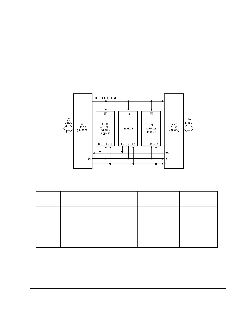
Figure 7 shows how two mi-
crocontrollers and several peripherals may be intercon-
nected using the MICROWIRE/PLUS arrangement.
Master MICROWIRE/PLUS Operation
In the MICROWIRE/PLUS Master mode of operation the
shift clock (SK) is generated internally. The MICROWIRE/
PLUS Master always initiates all data exchanges. (See
Fig-
ure 7). The MSEL bit in the CNTRL register must be set to
enable the SO and SK functions onto the G Port. The SO
and SK pins must also be selected as outputs by setting ap-
propriate bits in the Port G configuration register.
Table 4
summarizes the bit settings required for Master mode of op-
eration.
SLAVE MICROWIRE/PLUS OPERATION
In the MICROWIRE/PLUS Slave mode of operation the SK
clock is generated by an external source. Setting the MSEL
bit in the CNTRL register enables the SO and SK functions
onto the G Port. The SK pin must be selected as an input
and the SO pin is selected as an output pin by appropriately
setting up the Port G configuration register.
Table 4 summa-
rizes the settings required to enter the Slave mode of opera-
tion.
The user must set the BUSY flag immediately upon entering
the Slave mode. This will ensure that all data bits sent by the
Master will be shifted properly. After eight clock pulses the
BUSY flag will be cleared and the sequence may be re-
peated. (See
Figure 7.)
TABLE 4.
G4
Config.
Bit
G5
Config.
Bit
G4
Fun.
G5
Fun.
G6
Fun.
Operation
1
1
SO
Int.
SK
SI
MICROWIRE
Master
0
1
TRI-STATE
Int.
SK
SI
MICROWIRE
Master
1
0
SO
Ext.
SK
SI
MICROWIRE
Slave
0
0
TRI-STATE
Ext.
SK
SI
MICROWIRE
Slave
TIMER/COUNTER
The device has a powerful 16-bit timer with an associated
16-bit register enabling them to perform extensive timer
functions. The timer T1 and its register R1 are each orga-
nized as two 8-bit read/write registers. Control bits in the reg-
ister CNTRL allow the timer to be started and stopped under
software control. The timer-register pair can be operated in
one of three possible modes.
Table 5 details various timer
operating modes and their requisite control settings.
DS009103-12
FIGURE 6. MICROWIRE/PLUS Block Diagram
COP820C/COP840C
www.national.com
15
Functional Description
(Continued)
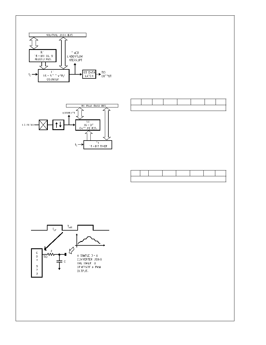
MODE 1. TIMER WITH AUTO-LOAD REGISTER
In this mode of operation, the timer T1 counts down at the in-
struction cycle rate. Upon underflow the value in the register
R1 gets automatically reloaded into the timer which contin-
ues to count down. The timer underflow can be programmed
to interrupt the microcontroller. A bit in the control register
CNTRL enables the TIO (G3) pin to toggle upon timer under-
flows. This allow the generation of square-wave outputs or
pulse width modulated outputs under software control. (See
Figure 8)
MODE 2. EXTERNAL COUNTER
In this mode, the timer T1 becomes a 16-bit external event
counter. The counter counts down upon an edge on the TIO
pin. Control bits in the register CNTRL program the counter
to decrement either on a positive edge or on a negative
edge. Upon underflow the contents of the register R1 are au-
tomatically copied into the counter. The underflow can also
be programmed to generate an interrupt. (See
Figure 8)
MODE 3. TIMER WITH CAPTURE REGISTER
Timer T1 can be used to precisely measure external fre-
quencies or events in this mode of operation. The timer T1
counts down at the instruction cycle rate. Upon the occur-
rence of a specified edge on the TIO pin the contents of the
timer T1 are copied into the register R1. Bits in the control
register CNTRL allow the trigger edge to be specified either
as a positive edge or as a negative edge. In this mode the
user can elect to be interrupted on the specified trigger edge.
(See
Figure 9.)
TABLE 5. Timer Operating Modes
CNTRL
Bits
7 6 5
Operation Mode
T Interrupt
Timer
Counts
On
0 0 0
External Counter W/Auto-Load Reg.
Timer Underflow
TIO Pos. Edge
0 0 1
External Counter W/Auto-Load Reg.
Timer Underflow
TIO Neg. Edge
0 1 0
Not Allowed
Not Allowed
Not Allowed
0 1 1
Not Allowed
Not Allowed
Not Allowed
1 0 0
Timer W/Auto-Load Reg.
Timer Underflow
t
C
1 0 1
Timer W/Auto-Load Reg./Toggle TIO Out
Timer Underflow
t
C
1 1 0
Timer W/Capture Register
TIO Pos. Edge
t
C
1 1 1
Timer W/Capture Register
TIO Neg. Edge
t
C
DS009103-13
FIGURE 7. MICROWIRE/PLUS Application
COP820C/COP840C
www.national.com
16
Functional Description
(Continued)
TIMER PWM APPLICATION
Figure 10 shows how a minimal component D/A converter
can be built out of the Timer-Register pair in the Auto-Reload
mode. The timer is placed in the "Timer with auto reload"
mode and the TIO pin is selected as the timer output. At the
outset the TIO pin is set high, the timer T1 holds the on time
and the register R1 holds the signal off time. Setting TRUN
bit starts the timer which counts down at the instruction cycle
rate. The underflow toggles the TIO output and copies the off
time into the timer, which continues to run. By alternately
loading in the on time and the off time at each successive in-
terrupt a PWM frequency can be easily generated.
Control Registers
CNTRL REGISTER (ADDRESS X'00EE)
The Timer and MICROWIRE/PLUS control register contains
the following bits:
SL1 & SL0 Select the MICROWIRE/PLUS clock divide-by
IEDG
External interrupt edge polarity select
(0 = rising edge, 1 = falling edge)
MSEL
Enable MICROWIRE/PLUS functions SO and
SK
TRUN
Start/Stop the Timer/Counter (1 = run, 0 = stop)
TC3
Timer input edge polarity select (0 = rising
edge, 1 = falling edge)
TC2
Selects the capture mode
TC1
Selects the timer mode
TC1
TC2
TC3
TRUN
MSEL
IEDG
SL1
SL0
Bit 7
Bit 0
PSW REGISTER (ADDRESS X'00EF)
The PSW register contains the following select bits:
GIE
Global interrupt enable
ENI
External interrupt enable
BUSY MICROWIRE/PLUS busy shifting
IPND
External interrupt pending
ENTI
Timer interrupt enable
TPND Timer interrupt pending
C
Carry Flag
HC
Half carry Flag
HC
C
TPND
ENTI
IPND
BUSY
ENI
GIE
Bit 7
Bit 0
Addressing Modes
REGISTER INDIRECT
This is the "normal" mode of addressing. The operand is the
memory addressed by the B register or X register.
DIRECT
The instruction contains an 8-bit address field that directly
points to the data memory for the operand.
IMMEDIATE
The instruction contains an 8-bit immediate field as the oper-
and.
REGISTER INDIRECT
(AUTO INCREMENT AND DECREMENT)
This is a register indirect mode that automatically increments
or decrements the B or X register after executing the instruc-
tion.
RELATIVE
This mode is used for the JP instruction, the instruction field
is added to the program counter to get the new program lo-
cation. JP has a range of from -31 to +32 to allow a one byte
relative jump (JP + 1 is implemented by a NOP instruction).
There are no 'pages' when using JP, all 15 bits of PC are
used.
DS009103-15
FIGURE 8. Timer/Counter Auto
Reload Mode Block Diagram
DS009103-14
FIGURE 9. Timer Capture Mode Block Diagram
DS009103-16
FIGURE 10. Timer Application
COP820C/COP840C
www.national.com
17
Memory Map
All RAM, ports and registers (except A and PC) are mapped
into data memory address space.
Address
Contents
COP820C Family
00 to 2F
On Chip RAM Bytes
30 to 7F
Unused RAM Address Space (Reads as all
Ones)
COP840C Family
00 to 6F
On Chip RAM Bytes
70 to 7F
Unused RAM Address Space (Reads as all
Ones)
COP820C and COP840C Families
80 to BF
Expansion Space for on Chip EERAM
C0 to CF
Expansion Space for I/O and Registers
D0 to DF
On Chip I/O and Registers
D0
Port L Data Register
D1
Port L Configuration Register
D2
Port L Input Pins (Read Only)
D3
Reserved for Port L
D4
Port G Data Register
D5
Port G Configuration Register
D6
Port G Input Pins (Read Only)
Address
Contents
COP820C and COP840C Families
D7
Port I Input Pins (Read Only)
D8≠DB
Reserved for Port C
DC
Port D Data Register
DD≠DF
Reserved for Port D
E0 to EF
On Chip Functions and Registers
E0≠E7
Reserved for Future Parts
E8
Reserved
E9
MICROWIRE/PLUS Shift Register
EA
Timer Lower Byte
EB
Timer Upper Byte
EC
Timer Autoload Register Lower Byte
ED
Timer Autoload Register Upper Byte
EE
CNTRL Control Register
EF
PSW Register
F0 to FF
On Chip RAM Mapped as Registers
FC
X Register
FD
SP Register
FE
B Register
Reading unused memory locations below 7FH will return all
ones. Reading other unused memory locations will return
undefined data.
Instruction Set
REGISTER AND SYMBOL DEFINITIONS
Registers
A
8-bit Accumulator register
B
8-bit Address register
X
8-bit Address register
SP
8-bit Stack pointer register
PC
15-bit Program counter register
PU
upper 7 bits of PC
PL
lower 8 bits of PC
C
1-bit of PSW register for carry
HC
Half Carry
GIE 1-bit of PSW register for global interrupt enable
Symbols
[B]
Memory indirectly addressed by B register
[X]
Memory indirectly addressed by X register
Mem
Direct address memory or [B]
MemI Direct address memory or [B] or Immediate data
Imm
8-bit Immediate data
Reg
Register memory: addresses F0 to FF (Includes B, X
and SP)
Bit
Bit number (0 to 7)
Loaded with
Exchanged with
Instruction Set
ADD
add
A
A + MemI
ADC
add with carry
A
A + MemI + C, C
Carry
HC
Half Carry
SUBC
subtract with carry
A
A + MemI +C, C
Carry
HC
Half Carry
AND
Logical AND
A
A and MemI
OR
Logical OR
A
A or MemI
XOR
Logical Exclusive-OR
A
A xor MemI
IFEQ
IF equal
Compare A and MemI, Do next if A = MemI
IFGT
IF greater than
Compare A and MemI, Do next if A
>
MemI
IFBNE
IF B not equal
Do next if lower 4 bits of B
Imm
DRSZ
Decrement Reg. ,skip if zero
Reg
Reg - 1, skip if Reg goes to 0
COP820C/COP840C
www.national.com
18

Instruction Set
(Continued)
Instruction Set (Continued)
SBIT
Set bit
1 to bit,
Mem (bit= 0 to 7 immediate)
RBIT
Reset bit
0 to bit,
Mem
IFBIT
If bit
If bit,
Mem is true, do next instr.
X
Exchange A with memory
A
Mem
LD A
Load A with memory
A
MemI
LD mem
Load Direct memory Immed.
Mem
Imm
LD Reg
Load Register memory Immed.
Reg
Imm
X
Exchange A with memory [B]
A
[B]
(B
B
±
1)
X
Exchange A with memory [X]
A
[X]
(X
X
±
1)
LD A
Load A with memory [B]
A
[B]
(B
B
±
1)
LD A
Load A with memory [X]
A
[X]
(X
X
±
1)
LD M
Load Memory Immediate
[B]
Imm (B
B
±
1)
CLRA
Clear A
A
0
INCA
Increment A
A
A + 1
DECA
Decrement A
A
A - 1
LAID
Load A indirect from ROM
A
ROM(PU,A)
DCORA
DECIMAL CORRECT A
A
BCD correction (follows ADC, SUBC)
RRCA
ROTATE A RIGHT THRU C
C
A7
...
A0
C
SWAPA
Swap nibbles of A
A7 ... A4
A3 ... A0
SC
Set C
C
1, HC
1
RC
Reset C
C
0, HC
0
IFC
If C
If C is true, do next instruction
IFNC
If not C
If C is not true, do next instruction
JMPL
Jump absolute long
PC
ii (ii = 15 bits, 0 to 32k)
JMP
Jump absolute
PC11..0
i (i = 12 bits)
JP
Jump relative short
PC
PC + r (r is -31 to +32, not 1)
JSRL
Jump subroutine long
[SP]
PL,[SP-1]
PU,SP-2,PC
ii
JSR
Jump subroutine
[SP]
PL,[SP-1]
PU,SP-2,PC11.. 0
i
JID
Jump indirect
PL
ROM(PU,A)
RET
Return from subroutine
SP+2,PL
[SP],PU
[SP-1]
RETSK
Return and Skip
SP+2,PL
[SP],PU
[SP-1],Skip next instruction
RETI
Return from Interrupt
SP+2,PL
[SP],PU
[SP-1],GIE
1
INTR
Generate an interrupt
[SP]
PL,[SP-1]
PU,SP-2,PC
0FF
NOP
No operation
PC
PC + 1
COP820C/COP840C
www.national.com
19
Instruction Set
(Continued)
Opcode
List
Bits
7
≠
4
F
E
D
C
B
A
9
876
5
4
3
2
1
0
Bits3
≠0
JP-15
JP-31
LD
0F0,
#i
DRSZ
0F0
RRCA
RC
ADC
A,
#i
ADC
A,
[B]
IFBIT
0,
[B]
*L
D
B
,
0F
IFBNE
0
JSR
0000
≠
00FF
JMP
0000
≠
00FF
JP+17
INTR
0
JP-14
JP-30
LD
0F1,
#i
DRSZ
0F1
*
S
C
SUBC
A,
#i
SUBC
A,
[B]
IFBIT
1,
[B]
*L
D
B
,
0E
IFBNE
1
JSR
0100
≠
01FF
JMP
0100
≠
01FF
JP+18
JP+2
1
JP-13
JP-29
LD
0F2,
#i
DRSZ
0F2
X
A,[X+]
X
A,[B+]
IFEQ
A,#i
IFEQ
A,[B]
IFBIT
2,[B]
*L
D
B
,
0D
IFBNE
2
JSR
0200
≠
02FF
JMP
0200
≠
02FF
JP+19
JP+3
2
JP-12
JP-28
LD
0F3,
#i
DRSZ
0F3
X
A,[X-]
X
A,[B-]
IFGT
A,#i
IFGT
A,[B]
IFBIT
3,[B]
*L
D
B
,
0C
IFBNE
3
JSR
0300
≠
03FF
JMP
0300
≠
03FF
JP+20
JP+4
3
JP-11
JP-27
LD
0F4,
#i
DRSZ
0F4
*
LAID
ADD
A,#i
ADD
A,[B]
IFBIT
4,[B]
CLRA
LD
B,
0B
IFBNE
4
JSR
0400
≠
04FF
JMP
0400
≠
04FF
JP+21
JP+5
4
JP-10
JP-26
LD
0F5,
#i
DRSZ
0F5
*
JID
AND
A,#i
AND
A,[B]
IFBIT
5,[B]
SWAPA
LD
B,
0A
IFBNE
5
JSR
0500
≠
05FF
JMP
0500
≠
05FF
JP+22
JP+6
5
JP-9
JP-25
LD
0F6,
#i
DRSZ
0F6
X
A,[X]
X
A,[B]
XOR
A,#i
XOR
A,[B]
IFBIT
6,[B]
DCORA
LD
B,
9
IFBNE
6
JSR
0600
≠
06FF
JMP
0600
≠
06FF
JP+23
JP+7
6
JP-8
JP-24
LD
0F7,
#i
DRSZ
0F7
*
*
OR
A,#i
OR
A,[B]
IFBIT
7,[B]
*
L
D
B
,
8
IFBNE
7
JSR
0700
≠
07FF
JMP
0700
≠
07FF
JP+24
JP+8
7
JP-7
JP-23
LD
0F8,
#i
DRSZ
0F8
NOP
*
L
D
A,#i
IFC
SBIT
0,[B]
RBIT
0,[B]
LD
B,
7
IFBNE
8
JSR
0800
≠
08FF
JMP
0800
≠
08FF
JP+25
JP+9
8
JP-6
JP-22
LD
0F9,
#i
DRSZ
0F9
*
*
*
IFNC
SBIT
1,[B]
RBIT
1,[B]
LD
B,
6
IFBNE
9
JSR
0900
≠
09FF
JMP
0900
≠
09FF
JP+26
JP+10
9
JP-5
JP-21
LD
0FA,
#i
DRSZ
0FA
LD
A,[X+]
LD
A,[B+]
LD
[B+],#i
INCA
SBIT
2,[B]
RBIT
2,[B]
LD
B,
5
IFBNE
0A
JSR
0A00
≠
0AFF
JMP
0A00
≠
0AFF
JP+27
JP+11
A
JP-4
JP-20
LD
0FB,
#i
DRSZ
0FB
LD
A,[X-]
LD
A,[B-]
LD
[B-],#i
DECA
SBIT
3,[B]
RBIT
3,[B]
LD
B,
4
IFBNE
0B
JSR
0B00
≠
0BFF
JMP
0B00
≠
0BFF
JP+28
JP+12
B
JP-3
JP-19
LD
0FC,
#i
DRSZ
0FC
LD
Md,#i
JMPL
X
A,Md
*
SBIT
4,[B]
RBIT
4,[B]
LD
B,
3
IFBNE
0C
JSR
0C00
≠
0CFF
JMP
0C00
≠
0CFF
JP+29
JP+13
C
JP-2
JP-18
LD
0FD,
#i
DRSZ
0FD
DIR
JSRL
LD
A,Md
RETSK
SBIT
5,[B]
RBIT
5,[B]
LD
B,
2
IFBNE
0D
JSR
0D00
≠
0DFF
JMP
0D00
≠
0DFF
JP+30
JP+14
D
JP-1
JP-17
LD
0FE,
#i
DRSZ
0FE
LD
A,[X]
LD
A,[B]
LD
[B],#i
RET
SBIT
6,[B]
RBIT
6,[B]
LD
B,
1
IFBNE
0E
JSR
0E00
≠
0EFF
JMP
0E00
≠
0EFF
JP+31
JP+15
E
JP-0
JP-16
LD
0FF,
#i
DRSZ
0FF
*
*
*
RETI
SBIT
7,[B]
RBIT
7,[B]
LD
B,
0
IFBNE
0F
JSR
0F00
≠
0FFF
JMP
0F00
≠
0FFF
JP+32
JP+16
F
Where,
i
i
s
the
immediate
data
Md
is
a
directly
addressed
memory
location
*
i
s
a
n
unused
opcode
(see
following
table)
COP820C/COP840C
www.national.com
20
Instruction Execution Time
Most instructions are single byte (with immediate addressing
mode instruction taking two bytes).
Most single instructions take one cycle time to execute.
Skipped instructions require x number of cycles to be
skipped, where x equals the number of bytes in the skipped
instruction opcode.
See the BYTES and CYCLES per INSTRUCTION table for
details.
Bytes and Cycles per
Instruction
The following table shows the number of bytes and cycles for
each instruction in the format of byte/cycle.
Arithmetic and Logic Instructions
[B]
Direct
Immed.
ADD
1/1
3/4
2/2
ADC
1/1
3/4
2/2
SUBC
1/1
3/4
2/2
AND
1/1
3/4
2/2
OR
1/1
3/4
2/2
XOR
1/1
3/4
2/2
IFEQ
1/1
3/4
2/2
[B]
Direct
Immed.
IFGT
1/1
3/4
2/2
IFBNE
1/1
DRSZ
1/3
SBIT
1/1
3/4
RBIT
1/1
3/4
IFBIT
1/1
3/4
The following table shows the instructions assigned to un-
used opcodes. This table is for information only. The opera-
tions performed are subject to change without notice. Do not
use these opcodes.
Unused
Opcode
Instruction
Unused
Opcode
Instruction
60
NOP
A9
NOP
61
NOP
AF
LD A, [B]
62
NOP
B1
C
HC
63
NOP
B4
NOP
67
NOP
B5
NOP
8C
RET
B7
X A, [X]
99
NOP
B9
NOP
9F
LD [B], #i
BF
LD A, [X]
A7
X A, [B]
A8
NOP
Memory Transfer Instructions
Register
Register Indirect
Indirect
Direct
Immed.
Auto Incr & Decr
[B]
[X]
[B+, B-]
[X+, X-]
X A,
*
1/1
1/3
2/3
1/2
1/3
LD A,
*
1/1
1/3
2/3
2/2
1/2
1/3
LD B,Imm
1/1
(If B
<
16)
LD B,Imm
2/3
(If B
>
15)
LD Mem,Imm
2/2
3/3
2/2
LD Reg,Imm
2/3
Note 20:
*
=
>
Memory location addressed by B or X or directly.
Instructions Using A & C
CLRA
1/1
INCA
1/1
DECA
1/1
LAID
1/3
DCORA
1/1
RRCA
1/1
SWAPA
1/1
SC
1/1
RC
1/1
IFC
1/1
IFNC
1/1
Transfer of Control Instructions
JMPL
3/4
JMP
2/3
JP
1/3
JSRL
3/5
JSR
2/5
JID
1/3
RET
1/5
RETSK
1/5
RETI
1/5
INTR
1/7
NOP
1/1
COP820C/COP840C
www.national.com
21

Option List
The mask programmable options are listed out below. The
options are programmed at the same time as the ROM pat-
tern to provide the user with hardware flexibility to use a va-
riety of oscillator configuration.
OPTION 1: CKI INPUT
= 1 Crystal
(CKI/10) CKO for crystal configuration
= 2 External (CKI/10) CKO available as G7 input
= 3 R/C
(CKI/10) CKO available as G7 input
OPTION 2: BONDING
= 1 28-pin DIP package
= 2 N.A.
= 3 20-pin DIP package
= 4 20-SO package
= 5 28-SO package
The following option information is to be sent to National
along with the EPROM.
Option Data
Option 1 Value__is: CKI Input
Option 2 Value__is: COP Bonding
COP8 Tools Overview
National is engaged with an international community of inde-
pendent 3rd party vendors who provide hardware and soft-
ware development tool support. Through National's interac-
tion and guidance, these tools cooperate to form a choice of
tools that fits each developer's needs.
This section provides a summary of the tool and develop-
ment kits currently available. Up-to-date information, selec-
tion guides, free tools, demos, updates, and purchase infor-
mation
can
be
obtained
at
our
web
site
at:
www.national.com/cop8.
SUMMARY OF TOOLS
COP8 Evaluation Software and Reference Designs
∑
COP8≠NSEVAL: Software Evaluation package for Win-
dows. A fully integrated evaluation environment for
COP8. Includes WCOP8 IDE evaluation version (Inte-
grated Development Environment), COP8-NSASM (Full
COP8 Assembler), COP8-MLSIM (COP8 Instruction
Level Simulator), COP8C Compiler Demo, DriveWay
TM
COP8 Device-Driver-Builder Demo, Manuals, Applica-
tions Software, and other COP8 technical information.
∑
COP8≠REF-xx: Reference Designs for COP8 Families.
Realtime hardware environment with a variety of func-
tions for demonstrating the various capabilities and fea-
tures of specific COP8 device families. Run Win 95 demo
reference software and exercise specific device capabili-
ties.
Includes PCB with pre-programmed COP8, 9v battery for
stand-alone operation, assembly listing, full applications
source code, BOM, and schematics.
(Add COP8-NSEVAL and an OTP programmer to imple-
ment your own software ideas in Assembly Code.)
COP8 Starter Kits and Hardware Target Solutions
∑
COP8-EVAL-xxx: A variety of Multifunction Evaluation,
Design Test, and Target Boards for COP8 Families. Real-
time target design environments with a selection of pe-
ripherals and features including multi I/O, LCD display,
keyboard, A/D, D/A, EEPROM, USART, LEDs, and
bread-board area. Quickly design, test, and implement a
custom target system (some target boards are stand-
alone, and ready for mounting into a standard enclosure),
or just evaluate and test your code. Includes COP8-
NSDEV with IDE and Assembler, software routines, refer-
ence designs, and source code (no p/s).
COP8 Software Development Languages and Integrated
Environments
∑
COP8-NSDEV: National's COP8 Software Development
package for Windows on CD. A fully Integrated Develop-
ment Environment for COP8. Includes a fully licensed
WCOP8 IDE, COP8-NSASM. Plus Manuals, Applications
Software, and other COP8 technical information.
∑
COP8C: ByteCraft - C Cross-Compiler and Code Devel-
opment System. Includes BCLIDE (Integrated Develop-
ment Environment) for Win32, editor, optimizing C Cross-
Compiler, macro cross assembler, BC-Linker, and
MetaLinktools support. (DOS/SUN versions available;
Compiler is linkable under WCOP8 IDE; Compatible with
DriveWay COP8)
∑
EWCOP8, EWCOP8-M, EWCOP8-BL: IAR - ANSI
C-Compiler and Embedded Workbench. (M version in-
cludes MetaLink debugger support) (BL version: 4k code
limit; no FP). A fully integrated Win32 IDE, ANSI
C-Compiler, macro assembler, editor, linker, librarian,
and C-Spy high-level simulator/debugger.
COP8 Development Productivity Tools
∑
DriveWay-COP8: Aisys Corporation - COP8 Peripherals
Code Generation tool. Automatically generates tested
and documented C or Assembly source code modules
containing I/O drivers and interrupt handlers for each on-
chip peripheral. Application specific code can be inserted
for customization using the integrated editor. (Compatible
with COP8-NSASM, COP8C, and WCOP8 IDE.)
∑
COP8-UTILS: COP8 assembly code examples, device
drivers, and utilities to speed up code development. (In-
cluded with COP8-NSDEV and COP8-NSEVAL.)
∑
WCOP8 IDE: KKD - COP8 IDE (Integrated Development
Environment). Supports COP8C, COP8-NSASM, COP8-
MLSIM, DriveWay COP8, and MetaLink debugger under
a common Windows Project Management environment.
Code development, debug, and emulation tools can be
launched from a single project window framework. (In-
cluded in COP8-NSDEV and COP8-NSEVAL.)
COP8 Hardware Debug Tools
∑
COP8xx-DM: Metalink COP8 Debug Module for non-
flash COP8 Families. Windows based development and
real-time in-circuit emulation tool, with 100 frame trace,
32k s/w breaks, Enhanced User Interface, MetaLinkDe-
bugger, and COP8 OTP Programmer with sockets. In-
cludes COP8-NSDEV, power supply, DIP and/or SMD
emulation cables and adapters.
COP820C/COP840C
www.national.com
22
COP8 Tools Overview
(Continued)
∑
IM-COP8: MetaLink iceMASTER
Æ
for non-flash COP8
devices. Windows based, full featured real-time in-circuit
emulator, with 4k trace, 32k s/w breaks, and MetaLink-
Windows Debugger. Includes COP8-NSDEV and power
supply. Package-specific probes and surface mount
adaptors are ordered separately. (Add COP8-PM and
adapters for OTP programming.)
COP8 Development and OTP Programming Tools
∑
COP8-PM: COP8 Development Programming Module.
Windows programming tool for COP8 OTP Families. In-
cludes 40 DIP programming socket, control software,
RS232 cable, and power supply. (SMD and 87Lxx pro-
gramming adapters are extra.)
∑
Development: Metalink's Debug Module includes devel-
opment device programming capability for COP8 de-
vices. Many other third-party programmers are approved
for development and engineering use.
∑
Production: Third-party programmers and automatic
handling equipment cover needs from engineering proto-
type and pilot production, to full production environments.
∑
Factory Programming: Factory programming available
for high-volume requirements.
WHERE TO GET TOOLS
Tools are ordered directly from the following vendors. Please go to the vendor's web site for current listings of distributors.
Vendor
Home Office
Electronic Sites
Other Main Offices
Aisys
U.S.A.: Santa Clara, CA
www.aisysinc.com
Distributors
1-408-327-8820
info
@
aisysinc.com
fax: 1-408-327-8830
Byte Craft
U.S.A.
www.bytecraft.com
Distributors
1-519-888-6911
info
@
bytecraft.com
fax: 1-519-746-6751
IAR
Sweden: Uppsala
www.iar.se
U.S.A.: San Francisco
+46 18 16 78 00
info
@
iar.se
1-415-765-5500
fax: +46 18 16 78 38
info
@
iar.com
fax: 1-415-765-5503
info
@
iarsys.co.uk
U.K.: London
info
@
iar.de
+44 171 924 33 34
fax: +44 171 924 53 41
Germany: Munich
+49 89 470 6022
fax: +49 89 470 956
ICU
Sweden: Polygonvaegen
www.icu.se
Switzeland: Hoehe
+46 8 630 11 20
support
@
icu.se
+41 34 497 28 20
fax: +46 8 630 11 70
support
@
icu.ch
fax: +41 34 497 28 21
KKD
Denmark:
www.kkd.dk
MetaLink
U.S.A.: Chandler, AZ
www.metaice.com
Germany: Kirchseeon
1-800-638-2423
sales
@
metaice.com
80-91-5696-0
fax: 1-602-926-1198
support
@
metaice.com
fax: 80-91-2386
bbs: 1-602-962-0013
islanger
@
metalink.de
www.metalink.de
Distributors Worldwide
National
U.S.A.: Santa Clara, CA
www.national.com/cop8
Europe: +49 (0) 180 530 8585
1-800-272-9959
support
@
nsc.com
fax: +49 (0) 180 530 8586
fax: 1-800-737-7018
europe.support
@
nsc.com
Distributors Worldwide
The following companies have approved COP8 program-
mers in a variety of configurations. Contact your local office
or distributor. You can link to their web sites and get the lat-
est listing of approved programmers from National's COP8
OTP Support page at: www.national.com/cop8.
Advantech; Dataman; EE Tools; Minato; BP Microsystems;
Data I/O; Hi-Lo Systems; ICE Technology; Lloyd Research;
Logical Devices; MQP; Needhams; Phyton; SMS; Stag Pro-
grammers; System General; Tribal Microsystems; Xeltek.
CUSTOMER SUPPORT
Complete product information and technical support is avail-
able from National's customer response centers, and from
our on-line COP8 customer support sites.
COP820C/COP840C
www.national.com
23
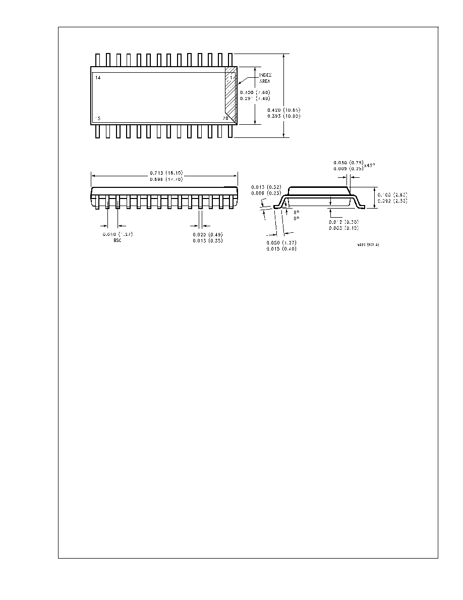
Physical Dimensions
inches (millimeters) unless otherwise noted
28-Lead Surface Mount Package (M)
Order Number COP820C-XXX/WM, COP840C-XXX/WM, COP920C-XXX/WM,
COP940C-XXX/WM, COP920CH-XXX/WM or COP940CH-XXX/WM
NS Package Number M28B
COP820C/COP840C
www.national.com
24
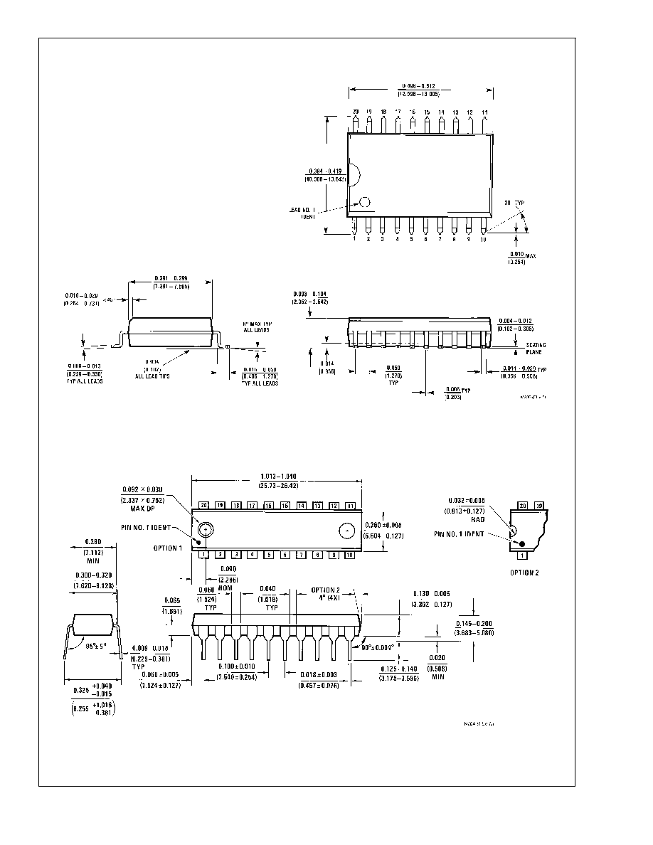
Physical Dimensions
inches (millimeters) unless otherwise noted (Continued)
20-Lead Surface Mount Package (M)
Order Number COP822C-XXX/WM, COP842C-XXX/WM, COP922C-XXX/WM,
COP942C-XXX/WM, COP922CH-XXX/WM or COP942CH-XXX/WM
NS Package Number M20B
20-Lead Molded Dual-in-Line Package (N)
Order Number COP622C-XXX/N, COP642C-XXX/N, COP822C-XXX/N, COP842C-XXX/N,
COP922C-XXX/N, COP942C-XXX/N, COP922CH-XXX/N or COP942CH-XXX/N
NS Package Number N20A
COP820C/COP840C
www.national.com
25
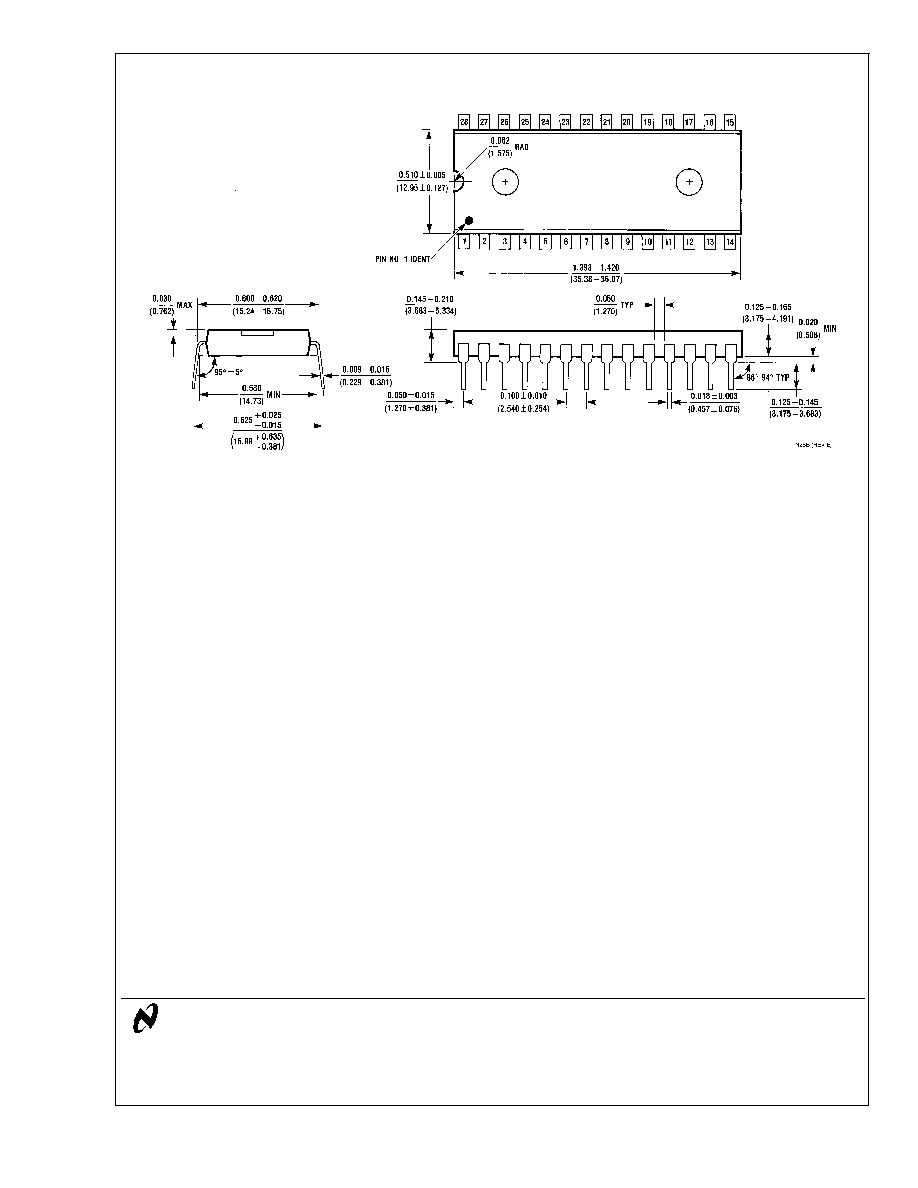
Physical Dimensions
inches (millimeters) unless otherwise noted (Continued)
LIFE SUPPORT POLICY
NATIONAL'S PRODUCTS ARE NOT AUTHORIZED FOR USE AS CRITICAL COMPONENTS IN LIFE SUPPORT
DEVICES OR SYSTEMS WITHOUT THE EXPRESS WRITTEN APPROVAL OF THE PRESIDENT AND GENERAL
COUNSEL OF NATIONAL SEMICONDUCTOR CORPORATION. As used herein:
1. Life support devices or systems are devices or
systems which, (a) are intended for surgical implant
into the body, or (b) support or sustain life, and
whose failure to perform when properly used in
accordance with instructions for use provided in the
labeling, can be reasonably expected to result in a
significant injury to the user.
2. A critical component is any component of a life
support device or system whose failure to perform
can be reasonably expected to cause the failure of
the life support device or system, or to affect its
safety or effectiveness.
National Semiconductor
Corporation
Americas
Tel: 1-800-272-9959
Fax: 1-800-737-7018
Email: support@nsc.com
National Semiconductor
Europe
Fax: +49 (0) 180-530 85 86
Email: europe.support@nsc.com
Deutsch Tel: +49 (0) 69 9508 6208
English
Tel: +44 (0) 870 24 0 2171
FranÁais Tel: +33 (0) 1 41 91 87 90
National Semiconductor
Asia Pacific Customer
Response Group
Tel: 65-2544466
Fax: 65-2504466
Email: ap.support@nsc.com
National Semiconductor
Japan Ltd.
Tel: 81-3-5639-7560
Email: nsj.crc@jksmtp.nsc.com
Fax: 81-3-5639-7507
www.national.com
28-Lead Molded Dual-in-Line Package (N)
Order Number COP620C-XXX/N, COP640C-XXX/N, COP820C-XXX/N, COP840C-XXX/N,
COP920C-XXX/N, COP940C-XXX/N, COP920CH-XXX/N or COP940CH-XXX/N
NS Package Number N28B
COP820C/COP840C
Family
CMOS
ROM
Based
Microcontrollers
with
1k
or
2k
Memory
National does not assume any responsibility for use of any circuitry described, no circuit patent licenses are implied and National reserves the right at any time without notice to change said circuitry and specifications.