COP820CJ/COP840CJ Family
8-Bit CMOS ROM Based Microcontrollers with 1k or 2k
Memory, Comparator and Brown Out Detector
General Description
The COP820CJ/840CJ Family ROM based microcontrollers
are integrated COP8
TM
Base core devices with 1k or 2k
memory, an Analog comparator and Brownout detection.
These single-chip CMOS devices are suited for lower-
functionality applications where power and voltage fluctua-
tions are a consideration. Pin and software compatible (no
Brownout; different Vcc range) 4k/32k OTP versions are
available (COP87LxxCJ/RJ Family) for pre-production, and
for use with a range of COP8 software and hardware devel-
opment tools.
Family features include an 8-bit memory mapped architec-
ture, 10MHz CKI with 1us instruction cycle, one multi-
function 16-bit timer/counter, MICROWIRE/PLUS
TM
serial
I/O, one analog comparator, power saving HALT mode,
MIWU, on-chip R/C oscillator capacitor (COP840CJ), high
current outputs, software selectable I/O options, WATCH-
DOG
TM
timer, modulator/timer, Brownout detector, Power on
Reset, 2.5v-6.0v operation, and 16/20/28 pin packages.
In this datasheet, the term COP820CJ refers to packages in-
cluding the COP820CJ, COP822CJ, and COP823CJ; and
COP840CJ refers to COP840CJ, COP842CJ, COP940CJ,
and COP942CJ.
Devices included in this data sheet are:
Device
Memory (bytes)
RAM (bytes)
I/O Pins
Packages
Temperature
Comments
COP820CJ
1k ROM
64
24
28 DIP/SOIC
-40 to +85∞C
COP822CJ
1k ROM
54
16
20 DIP/SOIC
-40 to +85∞C
COP823CJ
1k ROM
64
12
16 SOIC
-40 to +85∞C
COP840CJ
2k ROM
128
24
28 DIP/SOIC
-40 to +85∞C
Low EMI
COP940CJ
2k ROM
128
24
28 DIP/SOIC
-0 to +70∞C
2.5V-4.5V, CJH = 4V-6V
COP842CJ
2k ROM
128
16
20 DIP/SOIC
-40 to +85∞C
COP942CJ
2k ROM
128
16
20 DIP/SOIC
-0 to +70∞C
2.5V-4.5V, CJH = 4V-6V
Key Features
n
Multi-Input Wake Up (on the 8-bit Port L)
n
Brown out detector
n
Analog comparator
n
Modulator/timer (High speed PWM for IR transmission)
n
16-bit multi-function timer supporting
-- PWM mode
-- External event counter mode
-- Input capture mode
n
1024 or 2048 bytes of ROM
n
64 or 128 bytes of RAM
n
Quiet design (low radiated emissions)
n
Integrated capacitor for the R/C oscillator for COP840CJ
I/O Features
n
Software selectable I/O options (TRI-STATE
Æ
output,
push-pull output, weak pull-up input, high impedance
input)
n
High current outputs (8 pins)
n
Packages
-- 16 SO with 12 I/O pins for COP820CJ
-- 20 DIP/SO with 16 I/O pins
-- 28 DIP/SO with 24 I/O pins
n
Schmitt trigger inputs on Port G
n
MICROWIRE/PLUS serial I/O
CPU/Instruction Set Feature
n
1 µs instruction cycle time
n
Three multi-source vectored interrupts servicing
-- External interrupt with selectable edge
-- Timer interrupt
-- Software interrupt
n
8-bit Stack Pointer (SP) -- stack in RAM
n
Two 8-bit register indirect data memory pointers (B, X)
Fully Static CMOS
n
Low current drain (typically
<
1 µA)
n
Single supply operation: 2.5V to 6.0V
n
Temperature ranges: -0∞C to +70∞C and -40∞C to +85∞C
Development Support
n
Emulation and OTP devices
n
Real time emulation and full program debug offered by
MetaLink Development System
TRI-STATE
Æ
is a registered trademark of National Semiconductor Corporation.
COP8
TM
, MICROWIRE
TM
, MICROWIRE/PLUS
TM
and WATCHDOG
TM
are trademarks of National Semiconductor Corporation.
iceMASTER
Æ
is a registered trademark of MetaLink Corporation.
September 1999
COP820CJ/COP840CJ
Family
,
8-Bit
CMOS
ROM
Based
Microcontrollers
with
1k
or
2k
Memory
,
Comparator
and
Brown
Out
Detector
© 2000 National Semiconductor Corporation
DS011208
www.national.com
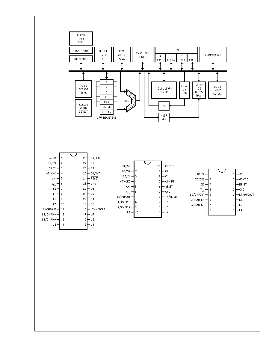
Block Diagram
Connection Diagrams
DS011208-1
2k ROM and 128 Bytes RAM for COP840CJ
FIGURE 1. Block Diagram
DS011208-3
Top View
Order Number COPCJ820-XXX/N or
COPCJ820-XXX/M,
Order Number COPCJ840-XXX/N or
COPCJ840-XXX/M,
Order Number COPCJ940-XXX/N or
COPCJ940-XXX/M
See NS Package Number N28B or
M28B
DS011208-4
Top View
Order Number COPCJ822-XXX/N or
COPCJ822-XXX/M
Order Number COPCJ842-XXX/N or
COPCJ842-XXX/M
Order Number COPCJ942-XXX/N or
COPCJ942-XXX/M
See NS Package Number N20A or
M20B
DS011208-5
Top View
Order Number COPCJ823-XXX/WM
See NS Package Number M16B
FIGURE 2. Connection Diagrams
COP820CJ/COP840CJ
Family
www.national.com
2
Absolute Maximum Ratings
(Note 1)
If Military/Aerospace specified devices are required,
please contact the National Semiconductor Sales Office/
Distributors for availability and specifications.
Supply Voltage (V
CC
)
7.0V
Voltage at any Pin
-0.3V to V
CC
+ 0.3V
Total Current into V
CC
pin (Source)
80 mA
Total Current out of GND pin (sink)
80 mA
Storage Temperature Range
-65∞C to +150∞C
Note 1:
Absolute maximum ratings indicate limits beyond which damage to
the device may occur.
DC and AC electrical specifications are not ensured when operating the de-
vice at absolute maximum ratings.
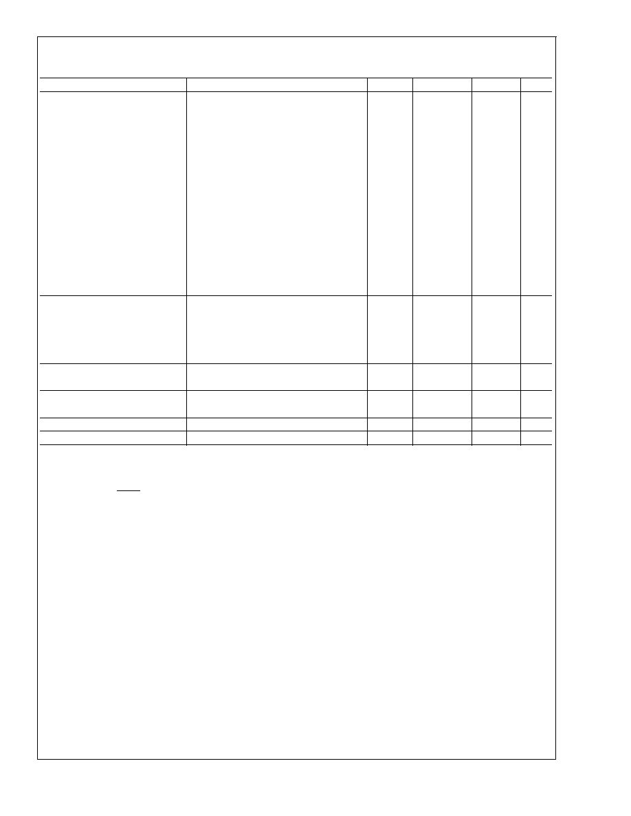
DC Electrical Characteristics
-0∞C
T
A
+ 70∞C for COP94x and -40∞C
T
A
+85∞C for all others
Parameter
Conditions
Min
Typ
Max
Units
Operating Voltage
Brown Out Disabled
2.5
6.0
V
COP94xCJ
Brown Out Disabled
2.5
4.5
V
COP94xCJH
Brown Out Disabled
4.5
6.0
V
Power Supply Ripple 1 (Note 2)
Peak to Peak
0.1 V
CC
V
Supply Current (Note 3)
CKI = 10 MHz
V
CC
= 6V, tc = 1 µs
6.0
mA
CKI = 4 MHz
V
CC
= 6V, tc = 2.5 µs
3.5
mA
CKI = 4 MHz
V
CC
= 4.0V, tc = 2.5 µs
2.0
mA
CKI = 1 MHz
V
CC
= 4.0V, tc = 10 µs
1.5
mA
HALT Current with Brown Out
Disabled (Note 4)
V
CC
= 6V, CKI = 0 MHz
<
1
10
µA
HALT Current with Brown Out
Enabled
V
CC
= 6V, CKI = 0 MHz
<
50
110
µA
COP840CJ Supply Current (Note
3)
CKI = 10 MHz, R = 2.2k
V
CC
= 6V, tc = 1 µs
8.0
mA
CKI = 4 MHz, R = 4.7k
V
CC
= 6V, tc = 2.5 µs
6.0
mA
CKI = 4 MHz, R = 4.7k
V
CC
= 4.5V, tc = 2.5 µs
2.5
mA
CKI = 1 MHz, R = 20k
V
CC
= 4.5V, tc = 10 µs
1.5
mA
HALT Current with Brown Out
Disabled
V
CC
= 6V, CKI = 0 MHz
<
2.2
8
µA
HALT Current with Brown Out
Enabled
V
CC
= 6V, CKI = 0 MHz
<
50
100
µA
Brown Out Trip Level (Brown Out
Enabled)
1.8
3.1
4.2
V
COP840CJ Brown Out Trip Level
(Brown Out Enabled)
1.9
3.1
3.9
V
INPUT LEVELS (V
IH
, V
IL
)
Reset, CKI:
Logic High
0.8 V
CC
V
Logic Low
0.2 V
CC
V
All Other Inputs
Logic High
0.7 V
CC
V
Logic Low
0.2 V
CC
V
Hi-Z Input Leakage
V
CC
= 6.0V
-2
+2
µA
Input Pullup Current
V
CC
= 6.0V, V
IN
= 0V
-40
-250
µA
L- and G-Port Hysteresis (Note 6)
COP840CJ
0.05 V
CC
0.35 V
CC
V
COP820CJ/COP840CJ
Family
www.national.com
4
DC Electrical Characteristics
(Continued)
-0∞C
T
A
+ 70∞C for COP94x and -40∞C
T
A
+85∞C for all others
Parameter
Conditions
Min
Typ
Max
Units
Output Current Levels
D Outputs:
Source
V
CC
= 4.5V, V
OH
= 3.8V
-0.4
mA
V
CC
= 2.5V, V
OH
= 1.8V
-0.2
mA
Sink
V
CC
= 4.5V, V
OL
= 1.0V
10
mA
V
CC
= 2.5V, V
OH
= 0.4V
2
mA
L4≠L7 Output Sink
V
CC
= 4.5V, V
OL
= 2.5V
15
mA
All Others
Source (Weak Pull-up Mode)
V
CC
= 4.5V, V
OH
= 3.2V
-10
-110
µA
V
CC
= 2.5V, V
OH
= 1.8V
-2.5
-33
µA
Source (Push-pull Mode)
V
CC
= 4.5V, V
OH
= 3.8V
-0.4
mA
V
CC
= 2.5V, V
OH
= 1.8V
-0.2
mA
Sink (Push-pull Mode)
V
CC
= 4.5V, V
OL
= 0.4V
1.6
mA
V
CC
= 2.5V, V
OL
= 0.4V
0.7
mA
TRI-STATE Leakage
-2.0
+2.0
µA
Allowable Sink/Source
Current Per Pin
D Outputs
15
mA
L4≠L7 (Sink)
20
mA
All Others
3
mA
Maximum Input Current
Room Temperature
±
100
mA
without Latchup (Note 5)
RAM Retention Voltage, V
r
500 ns Rise and
2.0
V
Fall Time (Min)
Input Capacitance
7
pF
Load Capacitance on D2
1000
pF
Note 2: Rate of voltage change must be less than 10 V/mS.
Note 3: Supply current is measured after running 2000 cycles with a square wave CKI input, CKO open, inputs at rails and outputs open.
Note 4: The HALT mode will stop CKI from oscillating in the RC and crystal configurations. HALT test conditions: L, and G0..G5 ports configured as outputs and set
high. The D port set to zero. All inputs tied to V
CC
. The comparator and the Brown Out circuits are disabled.
Note 5: Pins G6 and RESET are designed with a high voltage input network. These pins allow input voltages greater than V
CC
and the pins will have sink current
to V
CC
when biased at voltages greater than V
CC
(the pins do not have source current when biased at a voltage below V
CC
). The effective resistance to V
CC
is 750
(typical). These two pins will not latch up. The voltage at the pins must be limited to less than 14V.
COP820CJ/COP840CJ
Family
www.national.com
5