TL DD11299
COP8780CCOP8781CCOP8782C
8-Bit
One-Time
Programmable
(OTP)
Microcontroller
August 1996
COP8780C COP8781C COP8782C
8-Bit One-Time Programmable (OTP) Microcontroller
General Description
The COP8780C COP8781C and COP8782C are members
of the COPS
TM
8-bit microcontroller family They are fully
static microcontrollers fabricated using double-metal dou-
ble poly silicon gate microCMOS EPROM technology
These devices are available as UV erasable or One Time
Programmable (OTP) These low cost microcontrollers are
complete microcomputers containing all system timing in-
terrupt logic EPROM RAM and I O necessary to imple-
ment dedicated control functions in a variety of applications
Features include an 8-bit memory mapped architecture MI-
CROWIRE PLUS
TM
serial I O a 16-bit timer counter with
associated 16-bit autoreload capture register and a multi-
sourced interrupt Each I O pin has software selectable op-
tions to adapt the device to the specific application These
devices operate over a voltage range of 4 5V to 6 0V An
efficient regular instruction set operating at a 1 ms instruc-
tion cycle rate provides optimal throughput
The COP8780C COP8781C and COP8782C can be config-
ured to EMULATE the COP880C COP840C and COP820C
microcontrollers
Key Features
Y
16-bit multi-function timer supporting
PWM mode
External event counter mode
Input capture mode
Y
Crystal RC or External Oscillator user configurable
Y
4 kbytes on-chip OTP EPROM with security feature
Y
128 or 64 bytes of on-chip RAM user configurable
I O Features
Y
Memory-mapped I O
Y
Software selectable I O options (TRI-STATE
Push-
Pull Weak Pull-Up Input High Impedance input)
Y
Schmitt trigger inputs on Port G
Y
MICROWIRE PLUS serial I O
Y
Packages
44 PLCC OTP Emulates COP880C 36 I O pins
40 DIP OTP Emulates COP880C 36 I O pins
28 DIP OTP Emulates COP820C 840C 881C
24 I O pins
20 DIP OTP Emulates COP822C 842C 16 I O pins
28 SO 20 SO OTP
44 LDCC UV Erasable
40 CERDIP 28 CERDIP 20 CERDIP UV Erasable
CPU Instruction Set Features
Y
1 ms instruction cycle time
Y
Three multi-source interrupts servicing
External interrupt with selectable edge
Timer interrupt
Software interrupt
Y
Versatile and easy to use instruction set
Y
8-bit Stack Pointer (SP)
stack in RAM
Y
Two 8-bit Register Indirect Data Memory Pointers
(B and X)
Fully Static CMOS
Y
Low current drain (typically
k
1 mA)
Y
Extra-low current static HALT mode
Y
Single supply operation 4 5V to 6 0V
Y
Temperature range
b
40 C to
a
85 C
Development Support
Y
Emulation device for the COP880C
COP840C
and
COP820C
Y
Real-time emulation and full program debug offered by
MetaLink development system
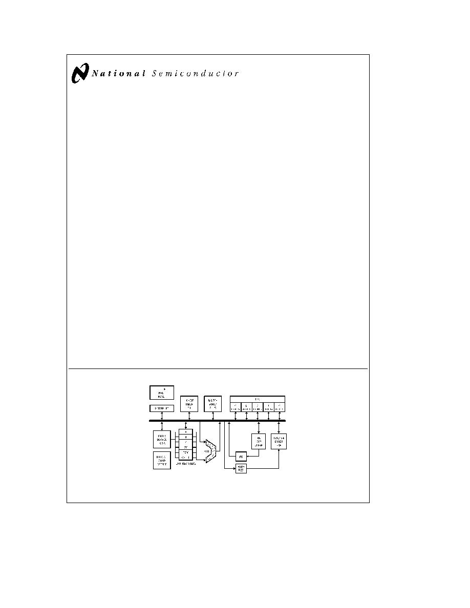
Block Diagram
TL DD 11299 � 1
FIGURE 1 Block Diagram
TRI-STATE
is a registered trademark of National Semiconductor Corporation
COPS
TM
microcontrollers MICROWIRE
TM
MICROWIRE PLUS
TM
and WATCHDOG
TM
are trademarks of National Semiconductor Corporation
iceMASTER
TM
is a trademark of MetaLink Corporation
C1996 National Semiconductor Corporation
RRD-B30M96 Printed in U S A
http
www national com
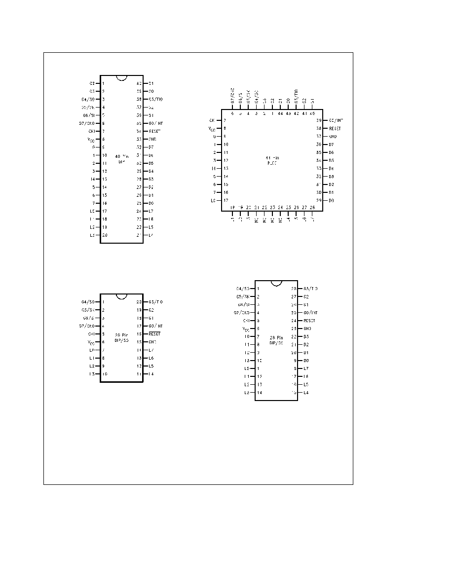
Connection Diagrams
TL DD 11299 � 3
Top View
Order Number COP8780C-XXX N or COP8780C-XXX J
See NS Package Number J40AQ or N40A
TL DD 11299 � 4
Top View
Order Number COP8780C-XXX V or COP8780C-XXX EL
See NS Package Number EL40C or V44A
TL DD 11299 � 5
Top View
Order Number COP78782C XXX J COP8782C-XXX N
or COP8782C-XXX WM
See NS Package Number J20AQ M20B or N20B
TL DD 11299 � 6
Top View
Order Number COP8781C-XXX J COP8781C-XXX N or
COP8781C-XXX WM
See NS Package Number J28AQ M28B or N28B
FIGURE 3 Connection Diagrams
http
www national com
2
COP8780C COP8781C COP8782C
Absolute Maximum Ratings
If Military Aerospace specified devices are required
please contact the National Semiconductor Sales
Office Distributors for availability and specifications
Supply Voltage (V
CC
)
7V
Programming Voltage V
PP
(RESET pin)
and ME (pin G6)
13 4V
Voltage at any Pin
b
0 3V to V
CC
a
0 3V
Total Current into V
CC
Pin (Source)
50 mA
Total Current out of GND Pin (Sink)
60 mA
Storage Temperature Range
b
65 C to
a
150 C
Note
Absolute maximum ratings indicate limits beyond
which damage to the device may occur DC and AC electri-
cal specifications are not ensured when operating the de-
vice at absolute maximum ratings
DC Electrical Characteristics
COP87XXC
b
40 C
s
T
A
s
a
85 C unless otherwise specified
Parameter
Condition
Min
Typ
Max
Units
Operating Voltage
4 5
6 0
V
Power Supply Ripple (Note 1)
Peak to Peak
0 1 V
CC
V
Supply Current
CKI
e
10 MHz (Note 2)
V
CC
e
6V t
c
e
1 ms
21
mA
HALT Current (Note 3)
V
CC
e
6V CKI
e
0 MHz
10
m
A
Input Levels
RESET CKI
Logic High
0 9 V
CC
V
Logic Low
0 1 V
CC
V
All Other Inputs
Logic High
0 7 V
CC
V
Logic Low
0 2 V
CC
V
Hi-Z Input Leakage
V
CC
e
6 0V
b
2
a
2
m
A
Input Pullup Current
V
CC
e
6 0V V
IN
e
0V
b
40
b
250
m
A
G Port Input Hysteresis
(Note 6)
0 05 V
CC
V
Output Current Levels
D Outputs
Source
V
CC
e
4 5V V
OH
e
3 8V
b
0 4
mA
Sink
V
CC
e
4 5V V
OL
e
1 0V
10
mA
All Others
Source (Weak Pull-Up)
V
CC
e
4 5V V
OH
e
3 2V
b
10
b
110
m
A
Source (Push-Pull Mode)
V
CC
e
4 5V V
OH
e
3 8V
b
0 4
mA
Sink (Push-Pull Mode)
V
CC
e
4 5V V
OL
e
0 4V
1 6
mA
TRI-STATE Leakage
b
2 0
a
2 0
m
A
Allowable Sink Source
Current per Pin
D Outputs (Sink)
15
mA
All Others
3
mA
Maximum Input Current (Notes 4 6)
Room Temp
g
200
mA
without Latchup (Room Temp)
RAM Retention Voltage Vr
2 0
V
(Note 5)
Input Capacitance
(Note 6)
7
pF
Load Capacitance on D2
(Note 6)
1000
pF
Note 1
Rate of voltage change must be less than 0 5V ms
Note 2
Supply current is measured after running 2000 cycles with a square wave CKI input CKO open inputs at rails and outputs open
Note 3
The HALT mode will stop CKI from oscillating in the RC and the crystal configurations Halt test conditions All Inputs tied to V
CC
L C and G port I O's
configured as outputs and programmed low D outputs programmed low the window for UV erasable packages is completely covered with an opaque cover to
prevent light from falling onto the die during HALT mode test Parameter refers to HALT mode entered via setting bit 7 of the G Port data register
Note 4
Pins G6 and RESET are designed with a high voltage input network for factory testing These pins allow input voltages greater than V
CC
and the pins will
have sink current to V
CC
when biased at voltages greater than V
CC
(the pins do not have source current when biased at a voltage below V
CC
) The effective
resistance to V
CC
is 750X (typ) These two pins will not latch up The voltage at the pins must be limited to less than 14V
Note 5
To maintain RAM integrity the voltage must not be dropped or raised instantaneously
Note 6
Parameter characterized but not tested
http
www national com
3
COP8780C COP8781C COP8782C
AC Electrical Characteristics
b
40 C
k
T
A
k
a
85 C unless otherwise specified
Parameter
Condition
Min
Typ
Max
Units
Instruction Cycle Time (t
c
)
Crystal Resonator or External Clock
V
CC
t
4 5V
1
DC
m
s
R C Oscillator Mode
V
CC
t
4 5V
3
DC
m
s
CKI Clock Duty Cycle (Note 7)
fr
e
Max
45
55
%
Rise Time (Note 7)
fr
e
10 MHz Ext Clock
12
ns
Fall Time (Note 7)
fr
e
10 MHz Ext Clock
8
ns
Inputs
t
SETUP
V
CC
t
4 5V
200
ns
t
HOLD
V
CC
t
4 5V
60
ns
Output Propagation Delay
C
L
e
100 pF R
L
e
2 2 kX
t
PD1
t
PD0
SO SK
V
CC
t
4 5V
0 7
m
s
All Others
V
CC
t
4 5V
1
m
s
MICROWIRE
TM
Setup Time (t
UWS)
20
ns
MICROWIRE Hold Time (t
UWH)
56
ns
MICROWIRE Output
Propagation Delay (t
UPD
)
220
ns
Input Pulse Width
Interrupt Input High Time
1
t
c
Interrupt Input Low Time
1
t
c
Timer Input High Time
1
t
c
Timer Input Low Time
1
t
c
Reset Pulse Width
1 0
m
s
Note 7
Parameter guaranteed by design but not tested
t
c
e
Instruction Cycle Time
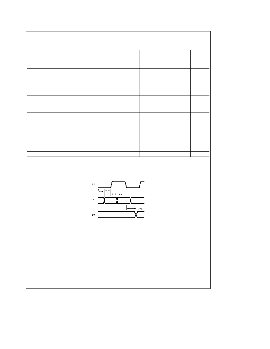
Timing Diagram
TL DD 10802 � 2
FIGURE 2 MICROWIRE PLUS Timing
http
www national com
4
Pin Descriptions
V
CC
and GND are the power supply pins
CKI is the clock input This can come from an external
source a R C generated oscillator or a crystal (in conjunc-
tion with CKO) See Oscillator description
RESET is the master reset input See Reset description
PORT I is an 8-bit Hi-Z input port The 28-pin device does
not have a full complement of PORT I pins The unavailable
pins are not terminated i e they are floating A read opera-
tion for these unterminated pins will return unpredictable
values The user must ensure that the software takes this
into account by either masking or restricting the accesses to
bit operations The unterminated PORT I pins will draw pow-
er only when addressed
PORT L is an 8-bit I O port
PORT C is a 4-bit I O port
Three memory locations are allocated for the L G and C
ports one each for data register configuration register and
the input pins Reading bits 4 � 7 of the C-Configuration reg-
ister data register and input pins returns undefined data
There are two registers associated with the L and C ports a
data register and a configuration register Therefore each L
and C I O bit can be individually configured under software
control as shown below
Config
Data
Ports L and C Setup
0
0
Hi-Z Input (TRI-STATE Output)
0
1
Input with Pull-Up (Weak One Output)
1
0
Push-Pull Zero Output
1
1
Push-Pull One Output
On the 20- and 28-pin parts it is recommended that all bits
of Port C be configured as outputs to minimize current
PORT G is an 8-bit port with 6 I O pins (G0 � G5) and 2 input
pins (G6 G7) All eight G-pins have Schmitt Triggers on the
inputs
There are two registers associated with the G port a data
register and a configuration register Therefore each G port
bit can be individually configured under software control as
shown below
Config
Data
Port G Setup
0
0
Hi-Z Input (TRI-STATE Output)
0
1
Input with Pull-Up (Weak One Output)
1
0
Push-Pull Zero Output
1
1
Push-Pull One Output
Since G6 and G7 are input only pins any attempt by the
user to configure them as outputs by writing a one to the
configuration register will be disregarded Reading the G6
and G7 configuration bits will return zeros The device will
be placed in the HALT mode by writing a one to the G7 bit in
the G-port data register
Six pins of Port G have alternate features
G0 INTR (an external interrupt)
G3 TIO (timer counter input output)
G4 SO (MICROWIRE PLUS serial data output)
G5 SK (MICROWIRE PLUS clock I O)
G6 SI (MICROWIRE PLUS serial data input)
G7 CKO crystal oscillator output (selected by programming
the ECON register) or HALT Restart general purpose
input
Pins G1 and G2 currently do not have any alternate func-
tions
PORT D is an 8-bit output port that is preset high when
RESET goes low Care must be exercised with the D2 pin
operation At reset the external load on this pin must en-
sure that the output voltage stay above 0 7 V
CC
to prevent
the chip from entering special modes Also keep the exter-
nal loading on D2 to less than 1000 pF
Functional Description
Figure 1 shows the block diagram of the internal architec-
ture Data paths are illustrated in simplified form to depict
how the various logic elements communicate with each oth-
er in implementing the instruction set of the device
ALU AND CPU REGISTERS
The ALU can do an 8-bit addition subtraction logical or
shift operation in one cycle time
There are five CPU registers
A is the 8-bit Accumulator register
PU is the upper 7 bits of the program counter (PC)
PL is the lower 8 bits of the program counter (PC)
B is the 8-bit address register can be auto incremented or
decremented
X is the 8-bit alternate address register can be incremented
or decremented
SP is the 8-bit stack pointer which points to the subroutine
interrupt stack in RAM The SP must be initialized with soft-
ware (usually to RAM address 06F Hex with 128 bytes of
on-chip RAM selected or to RAM address 02F Hex with 64
bytes of on-chip RAM selected) The SP is used with the
subroutine call and return instructions and with the inter-
rupts
B X and SP registers are mapped into the on-chip RAM
The B and X registers are used to address the on-chip RAM
The SP register is used to address the stack in RAM during
subroutine calls and returns
PROGRAM MEMORY
The device contains 4096 bytes of UV erasable or OTP
EPROM memory This memory is mapped in the program
memory address space from 0000 to 0FFF Hex The pro-
gram memory may contain either instructions or data con-
stants and is addressed by the 15-bit program counter (PC)
The program memory can be indirectly read by the LAID
(Load Accumulator Indirect) instruction for table lookup of
constant data
All locations in the EPROM program memory will contain
0FF Hex (all 1's) after the device is erased OTP parts are
shipped with all locations already erased to 0FF Hex Un-
used EPROM locations should always be programmed to 00
Hex so that the software trap can be used to halt runaway
program operation
The device can be configured to inhibit external reads of the
program memory This is done by programming the security
bit in the ECON (EPROM configuration) register to zero See
the ECON REGISTER section for more details
DATA MEMORY
The data memory address space includes on-chip RAM
I O and registers Data memory is addressed directly by
instructions or indirectly by means of the B X or SP point-
http
www national com
5