TL DD11208
COP820CJCOP822CJCOP823CJ
8-Bit
Microcontroller
with
Multi-Input
Wake
Up
and
Brown
Out
Detector
September 1996
COP820CJ COP822CJ COP823CJ 8-Bit Microcontroller
with Multi-Input Wake Up and Brown Out Detector
General Description
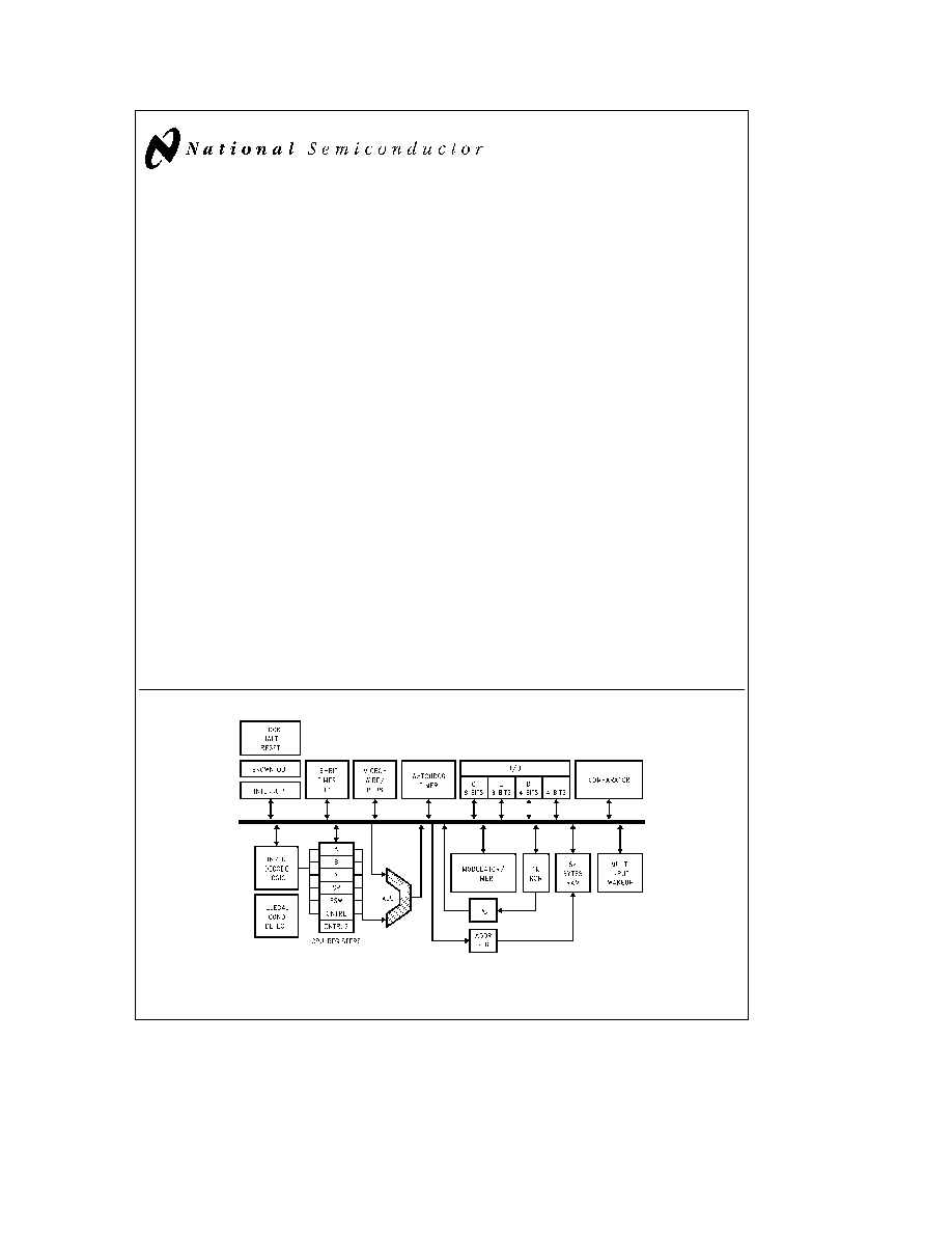
The COP820CJ is a member of the COP8
TM
8-bit Microcon-
troller family It is a fully static Microcontroller fabricated
using double-metal silicon gate microCMOS technology
This low cost Microcontroller is a complete microcomputer
containing all system timing interrupt logic ROM RAM and
I O necessary to implement dedicated control functions in a
variety of applications Features include an 8-bit memory
mapped architecture MICROWIRE
TM
serial I O a 16-bit
timer counter with capture register a multi-sourced inter-
rupt Comparator WATCHDOG
TM
Timer Modulator Timer
Brown out protection and Multi-Input Wakeup Each I O pin
has software selectable options to adapt the device to the
specific application The device operates over a voltage
range of 2 5V to 6 0V High throughput is achieved with an
efficient regular instruction set operating at a 1 ms per in-
struction rate
Key Features
Y
Multi-Input Wake Up (on the 8-bit Port L)
Y
Brown out detector
Y
Analog comparator
Y
Modulator timer (High speed PWM for IR transmission)
Y
16-bit multi-function timer supporting
PWM mode
External event counter mode
Input capture mode
Y
1024 bytes of ROM
Y
64 bytes of RAM
I O Features
Y
Memory mapped I O
Y
Software selectable I O options (TRI-STATE
output
push-pull output weak pull-up input high impedance
input)
Y
High current outputs (8 pins)
Y
Schmitt trigger inputs on Port G
Y
MICROWIRE PLUS
TM
serial I O
Y
Packages
16 SO with 12 I O pins
20 DIP SO with 16 I O pins
28 DIP SO with 24 I O pins
CPU Instruction Set Feature
Y
1 ms instruction cycle time
Y
Three multi-source vectored interrupts servicing
External interrupt with selectable edge
Timer interrupt
Software interrupt
Y
Versatile and easy to use instruction set
Y
8-bit Stack Pointer (SP)
stack in RAM
Y
Two 8-bit register indirect data memory pointers (B X)
Fully Static CMOS
Y
Low current drain (typically
k
1 mA)
Y
Single supply operation 2 5V to 6 0V
Y
Temperature range
b
40 C to
a
85 C
Development Support
Y
Emulation and OTP devices
Y
Real time emulation and full program debug offered by
MetaLink Development System
Block Diagram
TL DD 11208 ≠ 1
FIGURE 1 Block Diagram
TRI-STATE
is a registered trademark of National Semiconductor Corporation
COP8
TM
Microcontrollers MICROWIRE
TM
MICROWIRE PLUS
TM
and WATCHDOG
TM
are trademarks of National Semiconductor Corporation
iceMASTER
TM
is a trademark of MetaLink Corporation
C1996 National Semiconductor Corporation
RRD-B30M106 Printed in U S A
http
www national com
COP820CJ COP822CJ COP823CJ
Absolute Maximum Ratings
If Military Aerospace specified devices are required
please contact the National Semiconductor Sales
Office Distributors for availability and specifications
Supply Voltage (V
CC
)
7 0V
Voltage at any Pin
b
0 3V to V
CC
a
0 3V
Total Current into V
CC
pin (Source)
80 mA
Total Current out of GND pin (sink)
80 mA
Storage Temperature Range
b
65 C to
a
150 C
Note
Absolute maximum ratings indicate limits beyond
which damage to the device may occur
DC and AC electrical specifications are not ensured when
operating the device at absolute maximum ratings
DC Electrical Characteristics
b
40 C
s
T
A
s
a
85 C unless otherwise specified
Parameter
Conditions
Min
Typ
Max
Units
Operating Voltage
Brown Out Disabled
2 5
6 0
V
Power Supply Ripple 1 (Note 1)
Peak to Peak
0 1 V
CC
V
Supply Current (Note 2)
CKI
e
10 MHz
V
CC
e
6V tc
e
1 ms
6 0
mA
CKI
e
4 MHz
V
CC
e
6V tc
e
2 5 ms
3 5
mA
CKI
e
4 MHz
V
CC
e
4 0V tc
e
2 5 ms
2 0
mA
CKI
e
1 MHz
V
CC
e
4 0V tc
e
10 ms
1 5
mA
HALT Current with Brown Out
V
CC
e
6V CKI
e
0 MHz
k
1
10
m
A
Disbled (Note 3)
HALT Current with Brown Out
V
CC
e
6V CKI
e
0 MHz
k
50
110
m
A
Enabled
Brown Out Trip Level
1 8
3 1
4 2
V
(Brown Out Enabled)
INPUT LEVELS (V
IH
V
IL
)
Reset CKI
Logic High
0 8 V
CC
V
Logic Low
0 2 V
CC
V
All Other Inputs
Logic High
0 7 V
CC
V
Logic Low
0 2 V
CC
V
Hi-Z Input Leakage
V
CC
e
6 0V
b
2
a
2
m
A
Input Pullup Current
V
CC
e
6 0V V
IN
e
0V
b
40
b
250
m
A
L- and G-Port Hysteresis (Note 5)
0 35 V
CC
V
Output Current Levels
D Outputs
Source
V
CC
e
4 5V V
OH
e
3 8V
b
0 4
mA
V
CC
e
2 5V V
OH
e
1 8V
b
0 2
mA
Sink
V
CC
e
4 5V V
OL
e
1 0V
10
mA
V
CC
e
2 5V V
OH
e
0 4V
2
mA
L4 ≠ L7 Output Sink
V
CC
e
4 5V V
OL
e
2 5V
15
mA
All Others
Source (Weak Pull-up Mode)
V
CC
e
4 5V V
OH
e
3 2V
b
10
b
110
m
A
V
CC
e
2 5V V
OH
e
1 8V
b
2 5
b
33
m
A
Source (Push-pull Mode)
V
CC
e
4 5V V
OH
e
3 8V
b
0 4
mA
V
CC
e
2 5V V
OH
e
1 8V
b
0 2
mA
Sink (Push-pull Mode)
V
CC
e
4 5V V
OL
e
0 4V
1 6
mA
V
CC
e
2 5V V
OL
e
0 4V
0 7
mA
TRI-STATE Leakage
b
2 0
a
2 0
m
A
Allowable Sink Source
Current Per Pin
D Outputs
15
mA
L4 ≠ L7 (Sink)
20
mA
All Others
3
mA
http
www national com
2
DC Electrical Characteristics
b
40 C
s
T
A
s
a
85 C unless otherwise specified (Continued)
Parameter
Conditions
Min
Typ
Max
Units
Maximum Input Current
Room Temperature
g
100
mA
without Latchup (Note 4)
RAM Retention Voltage V
r
500 ns Rise and
2 0
V
Fall Time (Min)
Input Capacitance
7
pF
Load Capacitance on D2
1000
pF
Note 1
Rate of voltage change must be less than 10 V mS
Note 2
Supply current is measured after running 2000 cycles with a square wave CKI input CKO open inputs at rails and outputs open
Note 3
The HALT mode will stop CKI from oscillating in the RC and crystal configurations HALT test conditions L and G0 G5 ports configured as outputs and set
high The D port set to zero All inputs tied to V
CC
The comparator and the Brown Out circuits are disabled
Note 4
Pins G6 and RESET are designed with a high voltage input network These pins allow input voltages greater than V
CC
and the pins will have sink current to
V
CC
when biased at voltages greater than V
CC
(the pins do not have source current when biased at a voltage below V
CC
) The effective resistance to V
CC
is 750X
(typical) These two pins will not latch up The voltage at the pins must be limited to less than 14V
AC Electrical Characteristics
b
40 C
s
T
A
s
a
85 C unless otherwise specified
Parameter
Conditions
Min
Typ
Max
Units
Instruction Cycle Time (tc)
Crystal Resonator
4 5V
s
V
CC
s
6 0V
1
DC
m
s
2 5V
s
V
CC
s
4 5V
2 5
DC
m
s
R C Oscillator
4 5V
s
V
CC
s
6 0V
3
DC
m
s
2 5V
s
V
CC
s
4 5V
7 5
DC
m
s
V
CC
Rise Time when Using Brown Out
V
CC
e
0V to 6V
50
m
s
Frequency at Brown Out Reset
4
MHz
CKI Frequency For Modular Output
4
MHz
CKI Clock Duty Cycle (Note 5)
fr
e
Max
40
60
%
Rise Time (Note 5)
fr
e
10 MHz ext Clock
12
ns
Fall Time (Note 5)
fr
e
10 MHz ext Clock
8
ns
Inputs
t
Setup
4 5V
s
V
CC
s
6 0V
200
ns
2 5V
s
V
CC
s
4 5V
500
ns
t
Hold
4 5V
s
V
CC
s
6 0V
60
ns
2 5V
s
V
CC
s
4 5V
150
ns
Output Propagation Delay
R
L
e
2 2k CL
e
100 pF
t
PD1
t
PD0
SO SK
4 5V
s
V
CC
s
6 0V
0 7
m
s
2 5V
s
V
CC
s
4 5V
1 75
m
s
All Others
4 5V
s
V
CC
s
6 0V
1
m
s
2 5V
s
V
CC
s
4 5V
5
m
s
Input Pulse Width
Interrupt Input High Time
1
tc
Interrupt Input Low Time
1
tc
Timer Input High Time
1
tc
Timer Input Low Time
1
tc
MICROWIRE Setup Time (t
m
WS
)
20
ns
MICROWIRE Hold Time (t
m
WH
)
56
ns
MICROWIRE Output
220
ns
Propagation Delay (t
m
PD
)
Reset Pulse Width
1 0
m
s
Note 5
Parameter characterized but not production tested
http
www national com
3
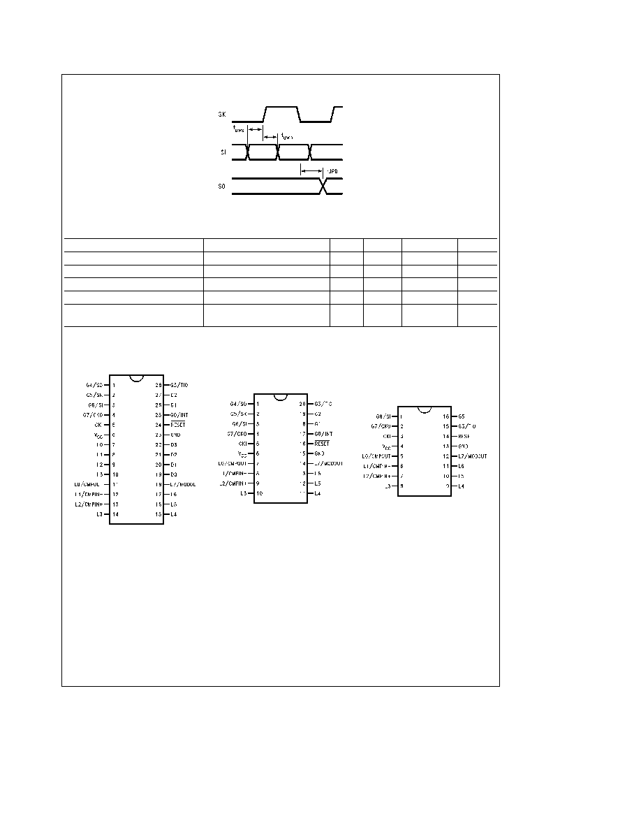
AC Electrical Characteristics
(Continued)
TL DD 11208 ≠ 2
FIGURE 2 MICROWIRE PLUS Timing
Comparator DC and AC Characteristics
4V
s
V
CC
s
6V
b
40 C
s
T
A
s
a
85 C (Note 1)
Parameters
Conditions
Min
Type
Max
Units
Input Offset Voltage
0 4V
k
V
IN
k
V
CC
b
1 5V
g
10
g
25
mV
Input Common Mode Voltage Range
0 4
V
CC
b
1 5
V
Voltage Gain
300k
V V
DC Supply Current (when enabled)
V
CC
e
6 0V
250
m
A
Response Time
TBD mV Step
1
m
s
TBD mV Overdrive 100 pF Load
Note 1
For comparator output current characteristics see L-Port specs
Connection Diagrams
TL DD 11208 ≠ 3
Top View
Order Number COPCJ820-XXX N or
COPCJ820-XXX WM
TL DD 11208 ≠ 4
Top View
Order Number COPCJ822-XXX N or
COPCJ822-XXX WM
TL DD 11208 ≠ 5
Top View
Order Number COPCJ823-XXX WM
FIGURE 3 Connection Diagrams
http
www national com
4
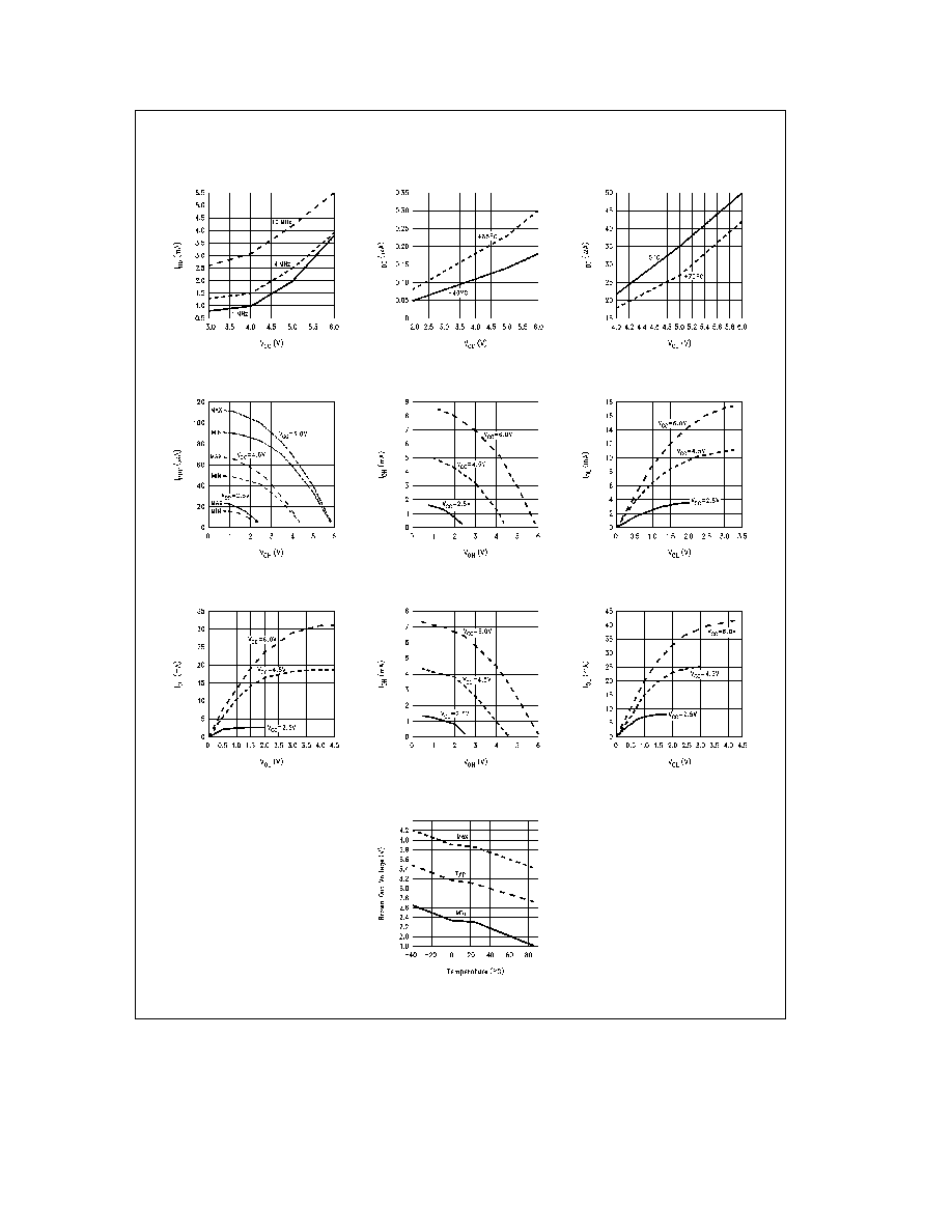
Typical Performance Characteristics
(Crystal Clock Option)
Dynamic
I
DD
vs V
CC
(Brown Out Disabled)
Halt
I
DD
vs V
CC
(Brown Out Enabled)
Halt
I
DD
vs V
CC
Pull-Up Source Current
Ports L G Weak
Source Current
Ports L G Push-Pull
Sink Current
Ports L G Push-Pull
Sink Current
Ports L4 ≠ L7
Port D Source Current
Port D Sink Current
vs Temperature
Brown Out Voltage
TL DD 11208 ≠ 28
http
www national com
5