COP87LxxCJ/RJ Family
8-Bit CMOS OTP Microcontrollers with 4k or 32k Memory
and Comparator
General Description
The COP87LxxCJ/RJ Family OTP (One Time Program-
mable) microcontrollers are integrated COP8
TM
Base core
devices with 4k or 32k memory, and an Analog comparator
(no brownout). These multi-chip CMOS devices are suited
for lower-functionality applications, and as pre-production
devices for a ROM design. Low cost, pin and software com-
patible (plus Brownout) 1k or 2k ROM versions are available
(COP820CJ/840CJ Family). Versions are available for use
with a range of COP8 software and hardware development
tools.
Family features include an 8-bit memory mapped architec-
ture, 10 MHz CKI with 1µs instruction cycle, three clock op-
tions (-1 = crystal; -2 = external; -3 = internal RC), one multi-
function 16-bit timer/counter, MICROWIRE/PLUS
TM
serial
I/O, one analog comparator, power saving HALT mode with
multi-sourced wakeup/interrupt capability, on-chip R/C oscil-
lator capacitor, high current outputs, software selectable I/O
options, WATCHDOG
TM
timer, modulator/timer, Power on
Reset, program code security, 2.7V to 5.5V operation and
20/28 pin packages.
In this datasheet, the term COP87L20CJ refers to the
COP87L20CJ, and COP87L22CJ. COP840CJ refers to the
COP87L40CJ,
COP87L42CJ,
COP87L40RJ,
and
COP87L42RJ.
Devices included in this datasheet are:
Device
Memory (bytes)
RAM (bytes)
I/O Pins
Packages
Temperature
COP87L20CJ
4k OTP EPROM
64
24
28 DIP/SOIC
-40 to +85∞C
COP87L22CJ
4k OTP EPROM
64
16
20 DIP/SOIC
-40 to +85∞C
COP87L40CJ
4k OTP EPROM
128
24
28 DIP/SOIC
-40 to +85∞C
COP87L42CJ
4k OTP EPROM
128
16
20 DIP/SOIC
-40 to +85∞C
COP87L40RJ
32k OTP EPROM
128
24
28 DIP/SOIC
-40 to +85∞C
COP87L42RJ
32k OTP EPROM
128
16
20 DIP/SOIC
-40 to +85∞C
Key Features
n
Multi-Input Wakeup (on the 8-bit Port L)
n
Analog comparator
n
Modulator/Timer (high speed PWM timer for IR
transmission)
n
16-bit multi-function timer supporting
-- PWM mode
-- External event counter mode
-- Input capture mode
n
Integrated capacitor for the R/C oscillator
n
4 or 32 kbyte on-board OTP EPROM with security
feature
n
64 or 128 bytes on-chip RAM
I/O Features
n
Software selectable I/O options (TRI-STATE
Æ
, Push-Pull,
Weak Pull-Up Input, High Impedance Input)
n
High current outputs (8 pins)
n
Schmitt trigger inputs on Port G
n
MICROWIRE/PLUS serial I/O
n
Packages:
-- 20 DIP/SO with 16 I/O pins
-- 28 DIP/SO with 24 I/O pins
CPU/Instruction Set Features
n
1 µs instruction cycle time
n
Three multi-source interrupts servicing
-- External interrupt with selectable edge
-- Timer interrupt
-- Software interrupt
n
Versatile and easy to use instruction set
n
8-bit stack pointer (SP) -- stack in RAM
n
Two 8-bit Register Indirect Data Memory Pointers (B and
X)
Fully Static CMOS
n
Low current drain (typically
<
1 µA)
n
Single supply operation: 2.7V to 5.5V
n
Temperature range: -40∞C to +85∞C
Development Support
n
Emulation device for the COP820CJ/COP840CJ
n
Real time emulation and full program debug offered by
MetaLink Development Systems
TRI-STATE
Æ
is a registered trademark of National Semiconductor Corporation.
COP8
TM
, MICROWIRE
TM
, MICROWIRE/PLUS
TM
and WATCHDOG
TM
are trademarks of National Semiconductor Corporation.
iceMASTER
Æ
is a registered trademark of MetaLink Corporation.
PRELIMINARY
September 1999
COP87LxxCJ/RJ
Family,
8-Bit
CMOS
OTP
Microcontrollers
with
4k
or
32k
Memory
and
Comparator
© 1999 National Semiconductor Corporation
DS012529
www.national.com
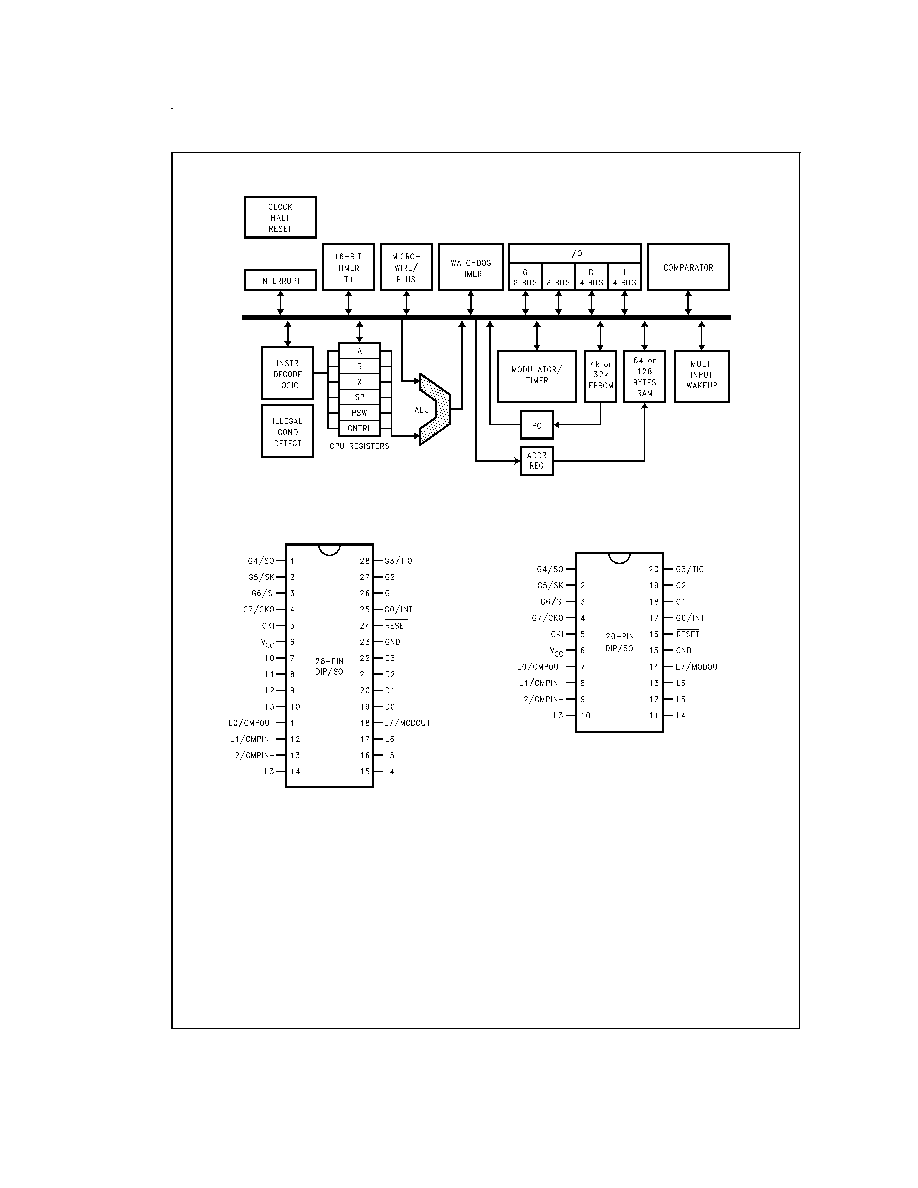
Block Diagram
Connection Diagrams
Note: -1 Crystal Oscillator
N - Brown out disabled
-2 External Oscillator
-3 R/C Oscillator
DS012529-1
FIGURE 1. Block Diagram
DS012529-2
Top View
Order Number
COP87L20CJN (-1N, -2N, -3N), or
COP87L20CJM(-1N, -2N, -3N), or
COP87L40CJN (-1N, -2N, -3N), or
COP87L40CJM (-1N, -2N, -3N), or
COP87L40RJN (-1N, -2N, -3N), or
COP87L40RJM (-1N, -2N, -3N)
See NS Package Number N28B or M28B
DS012529-3
Top View
Order Number
COP87L22CJN (-1N, -2N, -3N), or
COP87L22CJM(-1N, -2N, -3N), or
COP87L42CJN (-1N, -2N, -3N), or
COP87L42CJM (-1N, -2N, -3N), or
COP87L42RJN (-1N, -2N, -3N), or
COP87L42RJM (-1N, -2N, -3N)
See NS Package Number N20A or M20B
FIGURE 2. Connection Diagrams
www.national.com
2
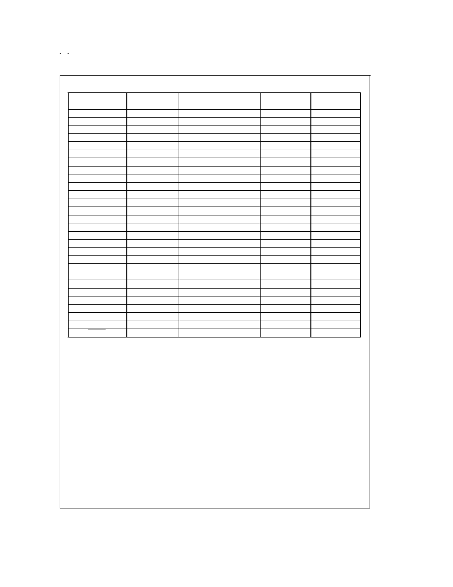
Pin Assignment
Port
Typ
ALT
20
28
Pin
Funct.
Pin
Pin
L0
I/O
MIWU/CMPOUT
7
11
L1
I/O
MIWU/CMPIN-
8
12
L2
I/O
MIWU/CMPIN+
9
13
L3
I/O
MIWU
10
14
L4
I/O
MIWU
11
15
L5
I/O
MIWU
12
16
L6
I/O
MIWU
13
17
L7
I/O
MIWU/MODOUT
14
18
G0
I/O
INTR
17
25
G1
I/O
18
26
G2
I/O
19
27
G3
I/O
TIO
20
28
G4
I/O
SO
1
1
G5
I/O
SK
2
2
G6
I
SI
3
3
G7
I
CKO
4
4
I0
I
7
I1
I
8
I2
I
9
I3
I
10
D0
O
19
D1
O
20
D2
O
21
D3
O
22
V
CC
6
6
GND
15
23
CKI
5
5
RESET
16
24
www.national.com
3
Absolute Maximum Ratings
(Note 1)
If Military/Aerospace specified devices are required,
please contact the National Semiconductor Sales Office/
Distributors for availability and specifications.
Supply Voltage (V
CC
)
7.0V
Voltage at any Pin
-0.3V to V
CC
+ 0.3V
Total Current into V
CC
pin (Source)
80 mA
Total Current out of GND pin (sink)
80 mA
Storage Temperature Range
-65∞C to +150∞C
Note 1:
Absolute maximum ratings indicate limits beyond which damage to
the device may occur. DC and AC electrical specifications are not ensured
when operating the device at absolute maximum ratings.
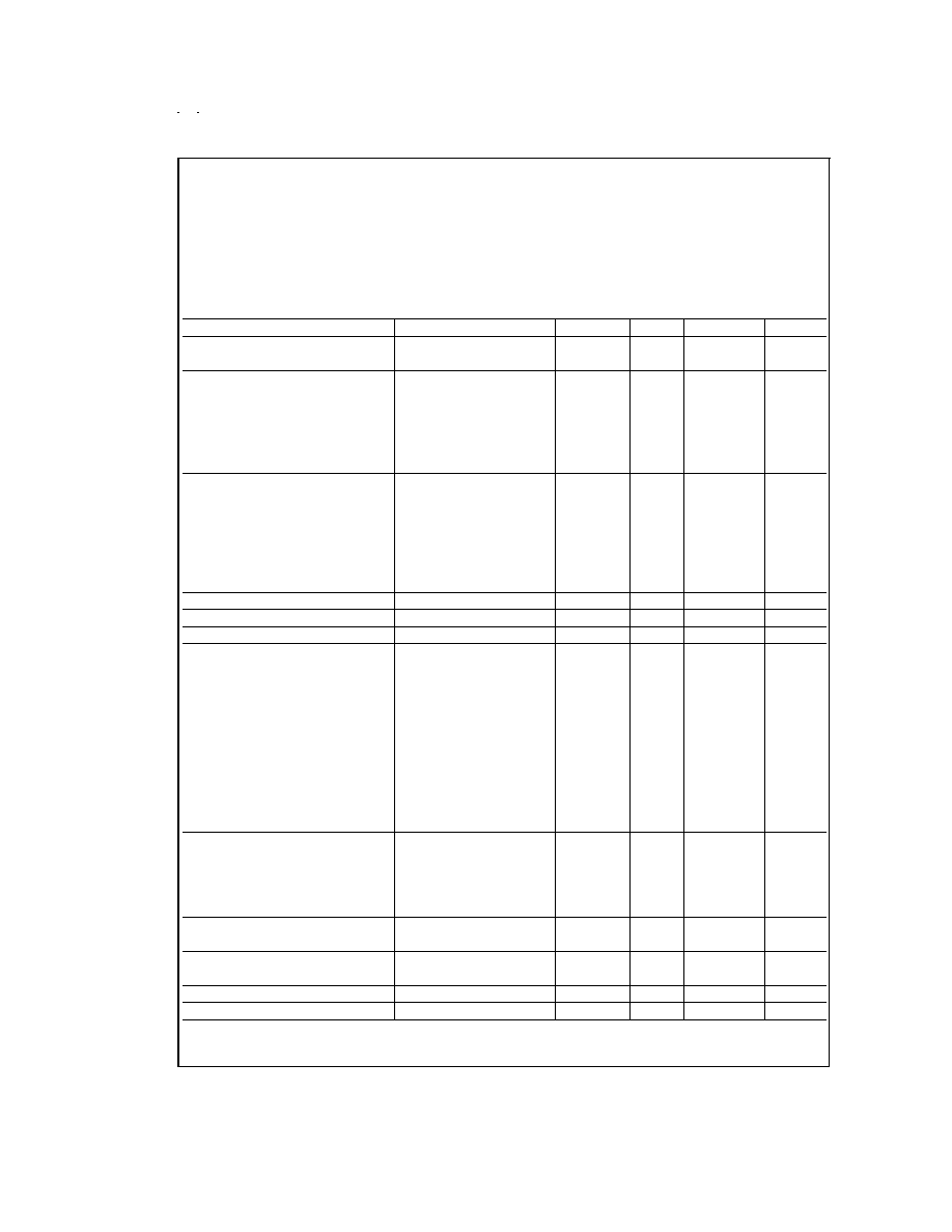
DC Electrical Characteristics
-40∞C
T
A
+85∞C unless otherwise specified
Parameter
Conditions
Min
Typ
Max
Units
Operating Voltage
2.7
5.5
V
Power Supply Ripple 1 (Note 2)
Peak to Peak
0.1 V
CC
V
Supply Current (Note 3)
CKI = 10 MHz
V
CC
= 5.5V, tc = 1 µs
12
mA
CKI = 4 MHz
V
CC
= 4.5V, tc = 2.5 µs
6.5
mA
CKI = 4 MHz (COP87L20CJ)
V
CC
= 4.0V, tc = 2.5 µs
10
mA
HALT Current (Note 4)
V
CC
= 5.5V, CKI = 0 MHz
12
µA
INPUT LEVELS (V
IH
, V
IL
)
Reset, CKI:
Logic High
0.8 V
CC
V
Logic Low
0.2 V
CC
V
All Other Inputs
Logic High
0.7 V
CC
V
Logic Low
0.2 V
CC
V
Hi-Z Input Leakage
V
CC
= 5.5V
-2
+2
µA
Input Pullup Current
V
CC
= 5.5V
-40
-250
µA
L- and G-Port Hysteresis (Note 7)
0.35 V
CC
V
Output Current Levels
D Outputs:
Source
V
CC
= 4.5V, V
OH
= 3.8V
-0.4
mA
Sink (Note 5)
V
CC
= 4.5V, V
OL
= 1.0V
10
mA
L4≠L7 Output Sink
V
CC
= 4.5V, V
OL
= 2.5V
15
mA
All Others
Source (Weak Pull-up Mode)
V
CC
= 4.5V, V
OH
= 3.2V
-10
-110
µA
Source (Push-pull Mode)
V
CC
= 4.5V, V
OH
= 3.8V
-0.4
mA
Sink (Push-pull Mode)
V
CC
= 4.5V, V
OL
= 0.4V
1.6
mA
(COP887L20CJ)
V
CC
= 5.5V, V
OL
= 0.4V
TRI-STATE Leakage
-2.0
+2.0
µA
Allowable Sink/Source
Current Per Pin
D Outputs
15
mA
L4≠L7 (Sink)
20
mA
All Others
3
mA
Maximum Input Current
Room Temperature
±
100
mA
without Latchup (Note 6)
RAM Retention Voltage, V
r
500 ns Rise and
2.0
V
Fall Time (Min)
Input Capacitance
7
pF
Load Capacitance on D2
1000
pF
Note 2: Rate of voltage change must be less than 10 V/mS.
Note 3: Supply current is measured after running 2000 cycles with a square wave CKI input, CKO open, inputs at rails and outputs open.
www.national.com
4
DC Electrical Characteristics
(Continued)
Note 4: The HALT mode will stop CKI from oscillating in the RC and crystal configurations by bringing CKI high. HALT test conditions: L, and G0..G5 ports configured
as outputs and set high. The D port set to zero. All inputs tied to V
CC
. The comparator is disabled.
Note 5: The user must guarantee that D2 pin does not source more than 10 mA during RESET. If D2 sources more than 10 mA during reset, the device will go into
programming mode.
Note 6: Pins G6 and RESET are designed with a high voltage input network. These pins allow input voltages greater than V
CC
and the pins will have sink current
to V
CC
when biased at voltages greater than V
CC
(the pins do not have source current when biased at a voltage below V
CC
). The effective resistance to V
CC
is 750
(typical). These two pins will not latch up. The voltage at the pins must be limited to less than 14V.
AC Electrical Characteristics
-40∞C
T
A
+85∞C unless otherwise specified
Parameter
Conditions
Min
Typ
Max
Units
Instruction Cycle Time (tc)
Crystal/Resonator
4.5V
V
CC
5.5V
1
DC
µs
R/C Oscillator
4.5V
V
CC
5.5V
2
DC
µs
CKI Clock Duty Cycle (Note 7)
fr = Max
40
60
%
Rise Time (Note 7)
fr = 10 MHz ext. Clock
12
ns
Fall Time (Note 7)
fr = 10 MHz ext. Clock
8
ns
Inputs
t
Setup
4.5V
V
CC
5.5V
200
ns
t
Hold
4.5V
V
CC
5.5V
60
ns
Output Propagation Delay
R
L
= 2.2k, CL = 100 pF
t
PD1
, t
PD0
SO, SK
4.5V
V
CC
5.5V
0.7
µs
All Others
4.5V
V
CC
5.5V
1
µs
Input Pulse Width
Interrupt Input High Time
1
tc
Interrupt Input Low Time
1
tc
Timer Input High Time
1
tc
Timer Input Low Time
1
tc
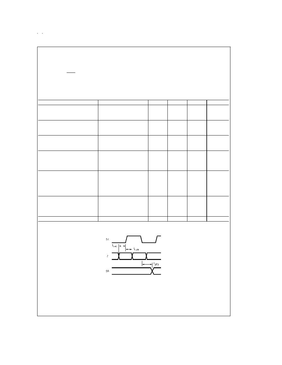
MICROWIRE
TM
Setup Time (t
µWS
)
20
ns
MICROWIRE Hold Time (t
µWH
)
56
ns
MICROWIRE Output
220
ns
Propagation Delay (t
µPD
)
Reset Pulse Width
1
µs
Note 7: Parameter characterized but not production tested.
DS012529-4
FIGURE 3. MICROWIRE/PLUS Timing
www.national.com
5