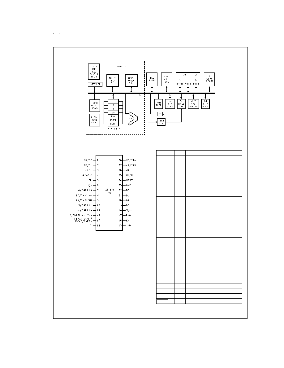
COP87L84BC
8-Bit CMOS OTP Microcontrollers with 16k Memory,
Comparators, and CAN Interface
General Description
The COP87L84BC OTP (One Time Programmable) micro-
controllers are highly integrated COP8
TM
Feature core de-
vices with 16k OTP EPROM memory and advanced features
including a CAN 2.0B (passive) interface and two Analog
comparators. These multi-chip CMOS devices are suited for
applications requiring a full featured controller with a CAN in-
terface, and 8-bit 39 kHz PWM timer, and as pre-production
devices for a masked ROM design. Pin and software com-
patible 2k ROM versions are available (COP884BC) with a
range of COP8 software and hardware development tools.
Features include an 8-bit memory mapped architecture, 10
MHz CKI (-XE = crystal oscillator) with 1µs instruction cycle,
one multi-function 16-bit timer/counter, 8-bit 39 kHz PWM
timer with 2 outputs, CAN 2.0B (passive) interface,
MICROWIRE/PLUS
TM
serial I/O, two Analog comparators,
two power saving HALT/IDLE modes, idle timer, MIWU, soft-
ware selectable I/O options, low EMI 4.5V to 5.5V operation,
and 28 pin packages.
Note: The companion devices with CAN interface, more I/O
and memory, A/D, and USART are the COP87L88EB/RB.
Device included in this datasheet is:
Device
Memory (bytes)
RAM (bytes)
I/O Pins
Packages
Temperature
COP87L84BC
16k OTP EPROM
64
18
28 SOIC
-40 to +85∞C
Key Features
n
CAN 2.0B (passive) Interface
n
One 16-bit timer, with two 16-bit registers supporting:
-- Processor Independent PWM mode
-- External Event counter mode
-- Input Capture mode
n
High speed, constant resolution 8-bit PWM/frequency
monitor timer with 2 output pins
n
16 kbytes on-board OTP EPROM with security feature
n
64 bytes on-board RAM
Additional Peripheral Features
n
Idle Timer
n
Multi-Input Wake Up (MIWU) with optional interrupts (7)
n
Two analog comparators
n
MICROWIRE/PLUS serial I/O
I/O Features
n
Memory mapped I/O
n
Software selectable I/O options (TRI-STATE
Æ
Output,
Push-Pull Output, Weak Pull-Up Input, High Impedance
Input)
n
Schmitt trigger inputs on ports G and L
n
Packages: 28 SO with 18 I/O pins
CPU/Instruction Set Features
n
1 µs instruction cycle time
n
Eleven multi-source vectored interrupts servicing
-- External Interrupt
-- Idle Timer T0
-- Timer T1 (with 2 Interrupts)
-- MICROWIRE/PLUS
-- Multi-Input Wake Up
-- Software Trap
-- PWM Timer
-- CAN Interface (with 3 interrupts)
n
Versatile and easy to use instruction set
n
8-bit Stack Pointer (SP) -- stack in RAM
n
Two 8-bit Register Indirect Data Memory Pointers
(B and X)
Fully Static CMOS
n
Two power saving modes: HALT and IDLE
n
Single supply operation: 4.5V≠5.5V
n
Temperature ranges: -40∞C to +85∞C
Development Support
n
Emulation device for COP884BC/COP885BC
n
Real time emulation and full program debug offered by
MetaLink Development Systems
COP8
TM
, and MICROWIRE/PLUS
TM
are trademarks of National Semiconductor Corporation.
TRI-STATE
Æ
is a registered trademark of National Semiconductor Corporation.
iceMASTER
Æ
is a registered trademark of MetaLink Corporation.
September 1999
COP87L84BC
8-Bit
CMOS
OTP
Microcontrollers
with
16k
Memory
,
Comparators,
and
CAN
Interface
© 1999 National Semiconductor Corporation
DS101137
www.national.com
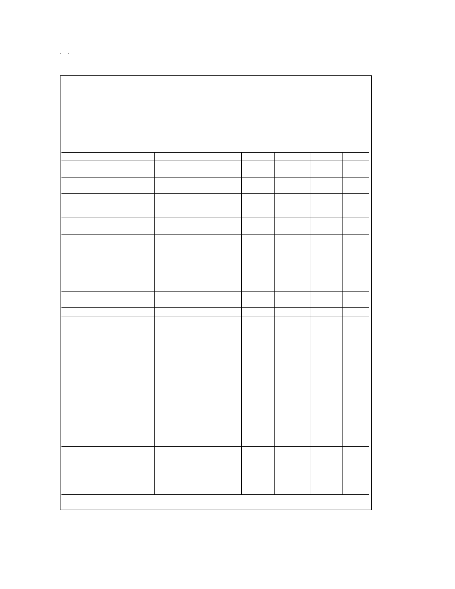
Absolute Maximum Ratings
(Note 1)
If Military/Aerospace specified devices are required,
please contact the National Semiconductor Sales Office/
Distributors for availability and specifications.
Supply Voltage (V
CC
)
6V
Voltage at Any Pin
-0.3V to V
CC
+0.3V
Total Current into V
CC
Pin (Source)
90 mA
Total Current out of GND Pin (Sink)
100 mA
Storage Temperature Range
-65∞C to +150∞C
Note 1: Absolute maximum ratings indicate limits beyond which damage to
the device may occur. DC and AC electrical specifications are not ensured
when operating the device at absolute maximum ratings.
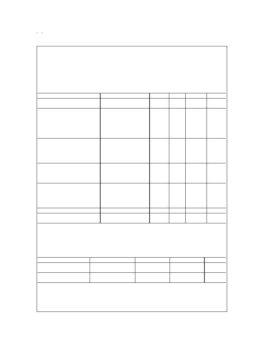
DC Electrical Characteristics
-40∞C
T
A
+85∞C
Parameter
Conditions
Min
Typ
Max
Units
Operating Voltage
4.5
5.5
V
Power Supply Ripple (Note 2)
Peak-to-Peak
0.1 V
CC
V
Supply Current
CKI = 10 MHz (Note 3)
V
CC
= 5.5V, t
c
= 1 µs
19
mA
HALT Current (Notes 4, 5)
V
CC
= 5.5V, CKI = 0 MHz
Power-On Reset Enabled
480
µA
Power-On Reset Disabled
380
µA
IDLE Current (Note 5)
CKI = 10 MHz
V
CC
= 5.5V, t
c
= 1 µs
5.5
mA
Input Levels (V
IH
, V
IL
)
Reset, CKI
Logic High
0.8 V
CC
V
Logic Low
0.2 V
CC
V
All Other Inputs
Logic High
0.7 V
CC
V
Logic Low
0.2 V
CC
V
Hi-Z Input Leakage
V
CC
= 5.5V
±
2
µA
Input Pull-up Current
V
CC
= 5.5V, V
IN
= 0V
-40
-250
µA
G and L Port Input Hysteresis
0.05 V
CC
V
Output Current Levels D Outputs
Source
V
CC
= 4.5V, V
OH
= 3.3V
-0.4
mA
Sink
V
CC
= 4.5V, V
OL
= 1.0V
10
mA
Comparator Output (L2, L6)
Source (Push-Pull)
V
CC
= 4.5V, V
OH
= 3.3V
-1.6
mA
Sink (Push-Pull)
V
CC
= 4.5V, V
OL
= 0.4V
1.6
mA
CAN Transmitter Outputs
Source (Tx1)
V
CC
= 4.5V, V
OH
= V
CC
- 0.1V
-1.5
mA
V
CC
= 4.5V, V
OH
= V
CC
- 0.6V
-10
mA
Sink (Tx0)
V
CC
= 4.5V, V
OL
= 0.1V
1.5
mA
V
CC
= 4.5V, V
OL
= 0.6V
10
mA
All Others
Source (Weak Pull-Up)
V
CC
= 4.5V, V
OH
= 2.7V
-10
-110
µA
Source (Push-Pull)
V
CC
= 4.5V, V
OH
= 3.3V
-0.4
mA
Sink (Push-Pull)
V
CC
= 4.5V, V
OL
= 0.4V
1.6
mA
TRl-STATE Leakage
V
CC
= 5.5V
±
2.0
µA
Allowable Sink/Source Current per
Pin
D Outputs (Sink)
15
mA
Tx0 (Sink)
30
mA
Tx1 (Source)
All Other
30
3
mA
mA
www.national.com
3
DC Electrical Characteristics
(Continued)
-40∞C
T
A
+85∞C
Parameter
Conditions
Min
Typ
Max
Units
Maximum Input Current
without Latchup
Room Temp
±
100
mA
RAM Retention Voltage, V
r
500 ns Rise and Fall Time
2.0
V
Input Capacitance
7
pF
Load Capacitance on D2
1000
pF
Note 2: Maximum rate of voltage change must be less than 0.5 V/ms
Note 3: Supply current is measured after running 2000 cycles with a square wave CKI input, CKO open, inputs at V
CC
or GND, and outputs open.
Note 4: The HALT mode will stop CKI from oscillating in the Crystal configurations. Halt test conditions: All inputs tied to V
CC
; L, and G port I/Os configured as outputs
and programmed low; D outputs programmed low. Parameter refers to HALT mode entered via setting bit 7 of the G Port data register. Part will pull up CKI during
HALT in crystal clock mode.
Note 5: HALT and IDLE current specifications assume CAN block and comparators are disabled.
www.national.com
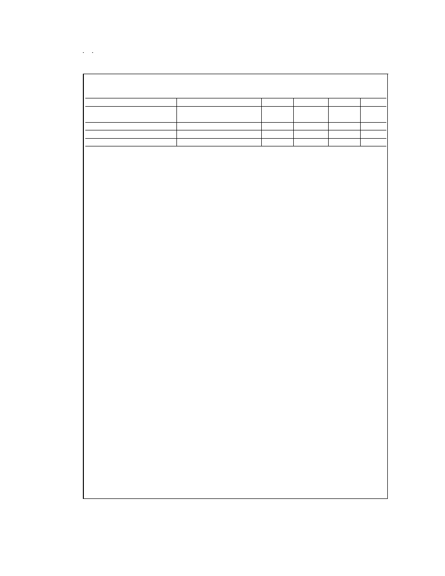
4
Absolute Maximum Ratings
(Note 1)
If Military/Aerospace specified devices are required,
please contact the National Semiconductor Sales Office/
Distributors for availability and specifications.
Supply Voltage (V
CC
)
6V
Voltage at Any Pin
-0.3V to V
CC
+0.3V
Total Current into V
CC
Pin (Source)
90 mA
Total Current out of GND Pin (Sink)
100 mA
Storage Temperature Range
-65∞C to +150∞C
Note 6: Absolute maximum ratings indicate limits beyond which damage to
the device may occur. DC and AC electrical specifications are not ensured
when operating the device at absolute maximum ratings.
AC Electrical Characteristics:
-40∞C
T
A
+85∞C
Parameter
Conditions
Min
Typ
Max
Units
Instruction Cycle Time (t
c
)
Crystal/Resonator
V
CC
4.5V
1.0
DC
µs
Inputs
t
SETUP
V
CC
4.5V
200
ns
t
HOLD
V
CC
4.5V
60
ns
PWM Capture Input
t
SETUP
V
CC
4.5V
30
ns
t
HOLD
V
CC
4.5V
70
ns
Output Propagation Delay
(t
PD1
, t
PD0
)
C
L
= 100 pF, R
L
= 2.2 k
SK, SO
V
CC
4.5V
0.7
µs
PWM Outputs
V
CC
4.5V
75
ns
All Others
V
CC
4.5V
1
µs
MICROWIRE
Setup Time (t
UWS
)
20
ns
Hold Time (t
UWH
)
56
ns
Output Prop Delay (t
UPD
)
220
ns
Input Pulse Width
Interrupt High Time
1
t
c
Interrupt Low Time
1
t
c
Timer 1,2 High Time
1
t
c
Timer 1,2 Low Time
1
t
c
Reset Pulse Width
1.0
µs
Power Supply Rise Time for Proper
50 µs
256*t
c
Operation of On-Chip RESET
Note 7: For device testing purposes of all AC parameters, V
OH
will be tested at 0.5*V
CC
.
Note 8: The output propagation delay is referenced to the end of the instruction cycle where the output change occurs.
Note 9: Parameter not tested.
Note 10: t
c
= Instruction Cycle Time.
On-Chip Voltage Reference:
-40∞C
T
A
+85∞C
Parameter
Conditions
Min
Max
Units
Reference Voltage
I
OUT
<
80 µA,
0.5 V
CC
-0.12
0.5 V
CC
+0.12
V
V
REF
V
CC
= 5V
Reference Supply Current,
I
OUT
= 0A, (No Load)
120
µA
I
DD
V
CC
= 5V (Note 11)
Note 11: Reference supply I
DD
is supplied for information purposes only, it is not tested.
www.national.com
5