COP87L88GD/RD Family
8-Bit CMOS OTP Microcontrollers with 16k or 32k
Memory and 8-Channel A/D with Prescaler
General Description
The COP87L88GD/RD OTP (One Time Programmable)
Family microcontrollers are highly integratet COP8
TM
Fea-
ture core devices with 16k or 32k memory and advanced
features including an A/D Converter. These multi-chip CMOS
devices are suited for applications requiring a full featured
controller with an 8-bit A/D converter, and as pre-production
devices for a masked ROM design. Pin and software com-
patible 16k ROM versions are available (COP888GD), as
well as a range of COP8 software and hardware develop-
ment tools.
Family features include an 8-bit memory mapped architec-
ture, 10 MHz CKI (-XE = crystal oscillator) with 1µs instruc-
tion
cycle,
three
multi-function
16-bit
timer/counters,
MICROWIRE/PLUS
TM
serial I/O, one 8-bit/8-channel A/D
converter with prescaler and both differential and single
ended modes, two power saving HALT/IDLE modes, MIWU,
idle timer, high current outputs, software selectable I/O op-
tions, WATCHDOG
TM
timer and Clock Monitor, 2.7V to 5.5V
operation, program code security, and 44 pin package.
Devices included in this datasheet are:
Device
Memory (bytes)
RAM (bytes)
I/O Pins
Packages
Temperature
COP87L88GD
16k EPROM
256
40
44 PLCC
-40 to +85∞C
COP87L88RD
32k EPROM
256
40
44 PLCC
-40 to +85∞C
Key Features
n
8-channel A/D converter with prescaler and both
differential and single ended modes
n
Idle Timer with 5 selectable Wake-Up periods
n
Three 16-bit timers, each with two 16-bit registers
supporting:
-- Processor Independent PWM mode
-- External Event counter mode
-- Input Capture mode
n
16 or 32 kbytes on-board OTP EPROM with security
feature
n
256 bytes on-board RAM
Additional Peripheral Features
n
Multi-Input Wakeup (MIWU) with optional interrupts (8)
n
WATCHDOG and clock monitor logic
n
MICROWIRE/PLUS serial I/O
I/O Features
n
Memory mapped I/O
n
Software selectable I/O options (TRI-STATE
Æ
Output,
Push-Pull Output, Weak Pull Up Input, High Impedance
Input)
n
Schmitt trigger inputs on ports G and L
n
Package:
-- 44 PLCC with 40 I/O pins
CPU/Instruction Set Features
n
1 µs instruction cycle time
n
Twelve multi-source vectored interrupts servicing
-- External Interrupt
-- Idle Timer T0
-- Three Timers (each with 2 Interrupts)
-- MICROWIRE/PLUS
-- Multi-Input Wake Up
-- Software Trap
-- Default VIS (default interrupt)
n
Versatile and easy to use instruction set
n
8-bit Stack Pointer (SP) ≠ stack in RAM
n
Two 8-bit Register Indirect Data Memory Pointers (B
and X)
Fully Static CMOS
n
Two power saving modes: HALT and IDLE
n
Single supply operation: 2.7V to 5.5V
n
Temperature range: -40∞C to +85∞C
Development Support
n
Emulation device for COP888GD
n
Real time emulation and full program debug offered by
MetaLink Development System
TRI-STATE
Æ
is a registered trademark of National Semiconductor Corporation.
MICROWIRE/PLUS
TM
, COP8
TM
, MICROWIRE
TM
and WATCHDOG
TM
are trademarks of National Semiconductor Corporation.
iceMASTER
Æ
is a registered trademark of MetaLink Corporation.
September 1999
COP87L88GD/RD
Family
8-Bit
CMOS
OTP
Microcontrollers
with
16k
or
32k
Memory
and
8-Channel
A/D
with
Prescaler
© 2000 National Semiconductor Corporation
DS012526
www.national.com
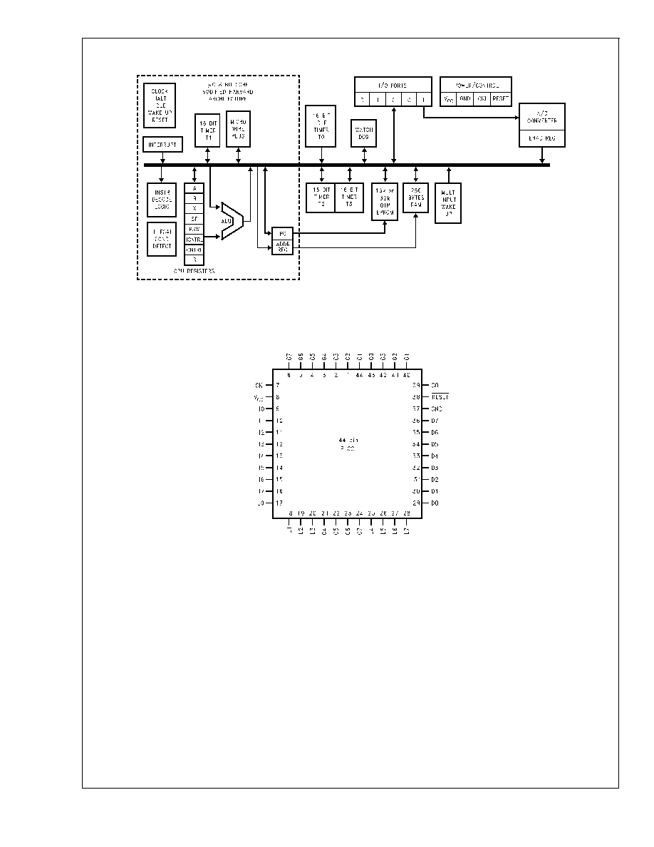
Block Diagram
Connection Diagrams
DS012526-1
FIGURE 1. Block Diagram
Plastic Chip Carrier
DS012526-2
Note: -X Crystal Oscillator
-E Halt Mode Enabled
Top View
Order Number COP87L88RDV-XE,
or COP87L88GDV-XE
See NS Plastic Chip Package Number V44A
FIGURE 2. Connection Diagrams
COP87L88GD/RD
Family
www.national.com
2
Connection Diagrams
(Continued)
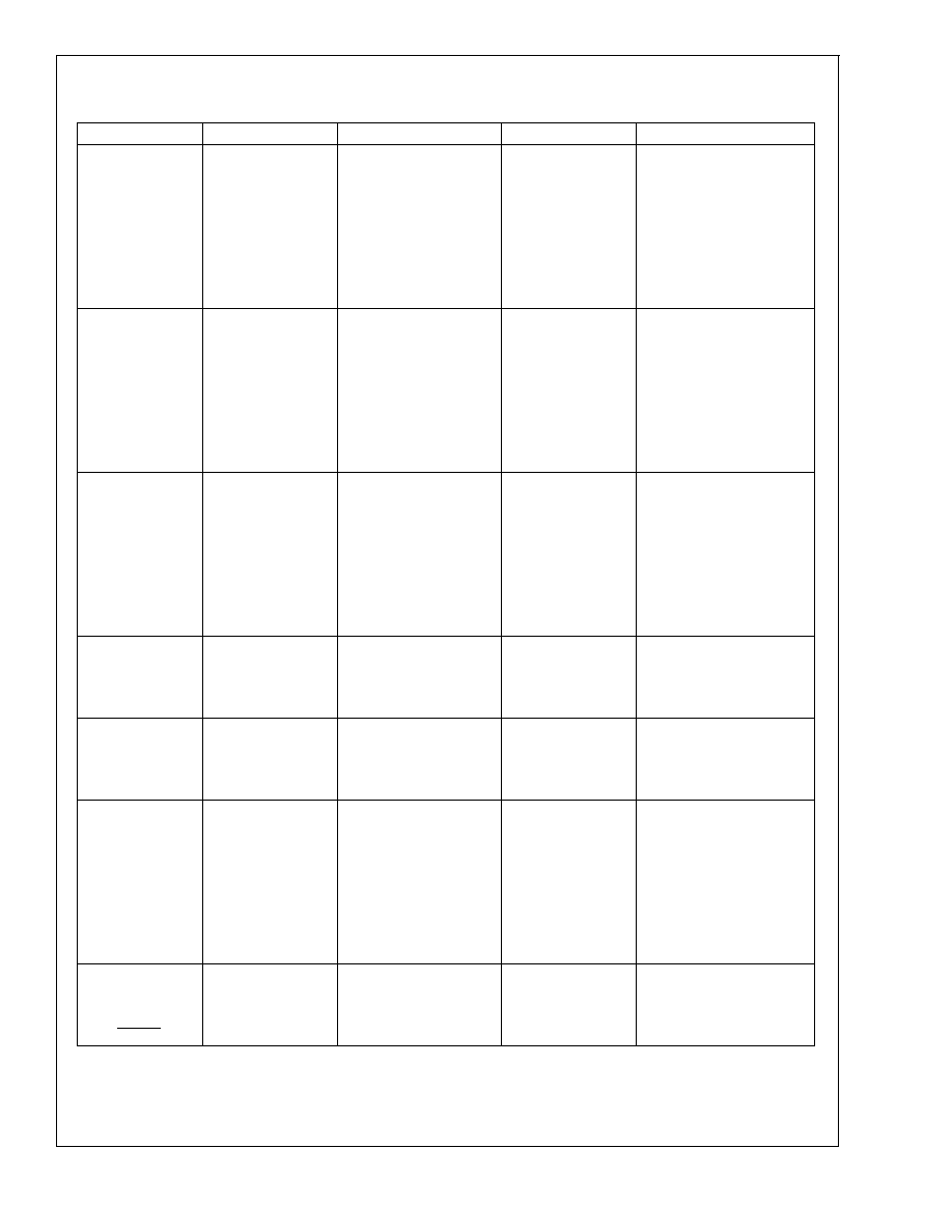
Pinouts for 40- and 44-Pin Packages
Port
Type
Alt. Fun
Alt. Fun
44-Pin Package
L0
I/O
MIWU
17
L1
I/O
MIWU
18
L2
I/O
MIWU
19
L3
I/O
MIWU
20
L4
I/O
MIWU
T2A
25
L5
I/O
MIWU
T2B
26
L6
I/O
MIWU
T3A
27
L7
I/O
MIWU
T3B
28
G0
I/O
INT
39
G1
WDOUT
40
G2
I/O
T1B
41
G3
I/O
T1A
42
G4
I/O
SO
3
G5
I/O
SK
4
G6
I
SI
5
G7
I/CKO
HALT Restart
6
D0
O
29
D1
O
30
D2
O
31
D3
O
32
D4
O
33
D5
O
34
D6
O
35
D7
O
36
I0
I
ACH0
9
I1
I
ACH1
10
I2
I
ACH2
11
I3
I
ACH3
12
I4
I
ACH4
13
I5
I
ACH5
14
I6
I
ACH6
15
I7
I
ACH7
16
C0
I/O
43
C1
I/O
44
C2
I/O
1
C3
I/O
2
C4
I/O
21
C5
I/O
22
C6
I/O
23
C7
I/O
24
V
CC
8
GND
37
CKI
7
RESET
38
COP87L88GD/RD
Family
www.national.com
3
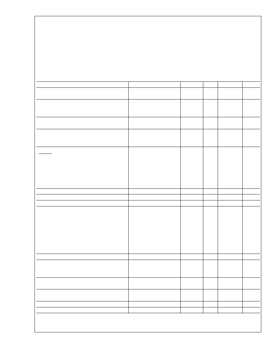
Absolute Maximum Ratings
(Note 1)
If Military/Aerospace specified devices are required,
please contact the National Semiconductor Sales Office/
Distributors for availability and specifications.
Supply Voltage (V
CC
)
7V
Voltage at Any Pin
-0.3V to V
CC
+ 0.3V
Total Current into V
CC
Pin
(Source)
100 mA
Total Current out of GND Pin
(Sink)
110 mA
Storage Temperature Range
-65∞C to +140∞C
Note 1:
Absolute maximum ratings indicate limits beyond which damage to
the device may occur. DC and AC electrical specifications are not ensured
when operating the device at absolute maximum ratings.
DC Electrical Characteristics
-40∞C
T
A
+85∞C unless otherwise specified
Parameter
Conditions
Min
Typ
Max
Units
Operating Voltage
2.7
5.5
V
Power Supply Ripple (Note 3)
Peak-to-Peak
0.1 V
CC
V
Supply Current (Note 4)
CKI = 10 MHz
V
CC
= 5.5V, t
c
= 1 µs
20
mA
CKI = 4 MHz
V
CC
= 4.0V, t
c
= 2.5 µs
10
mA
HALT Current (Note 5)
V
CC
= 5.5V, CKI = 0 MHz
12
µA
V
CC
= 4.0V, CKI = 0 MHz
10
µA
IDLE Current (Note 4)
CKI = 10 MHz
V
CC
= 5.5V, t
c
= 1 µs
1.2
mA
CKI = 4 MHz
V
CC
= 4.0V, t
c
= 2.5 µs
1
mA
Input Levels
RESET , CKI
Logic High
0.8 V
CC
V
Logic Low
0.2 V
CC
V
All Other Inputs (L0-L7, G0-G6, C0-C7, I0-I7)
Logic High
0.7 V
CC
V
Logic Low
0.2 V
CC
V
Hi-Z Input Leakage
V
CC
= 5.5V
-2
+2
µA
Input Pullup Current
V
CC
= 5.5V, V
IN
= 0V
-40
-250
µA
G and L Port Input Hysteresis (Note 9)
0.35 V
CC
V
Output Current Levels
D Outputs
Source
V
CC
= 4.5V, V
OH
= 3.3V
-0.4
mA
Sink (Note 6)
V
CC
= 4.5V, V
OL
= 1V
10
mA
All Others
Source (Weak Pull-Up Mode)
V
CC
= 4.5V, V
OH
= 2.7V
-10
-100
µA
Source (Push-Pull Mode)
V
CC
= 4.5V, V
OH
= 3.3V
-0.4
mA
Sink (Push-Pull Mode)
V
CC
= 4.5V, V
OL
= 0.4V
1.6
mA
TRI-STATE Leakage
V
CC
= 5.5V
-2
+2
µA
Allowable Sink/Source Current per Pin
D Outputs (Sink)
15
mA
All others
3
mA
Maximum Input Current
Room Temp
±
100
mA
without Latchup (Notes 7, 9)
RAM Retention Voltage, V
r
500 ns Rise
2
V
and Fall Time (min)
Input Capacitance
7
pF
Load Capacitance on D2
1000
pF
COP87L88GD/RD
Family
www.national.com
4
AC Electrical Characteristics
-40∞C
T
A
+85∞C unless otherwise specified
Parameter
Conditions
Min
Typ
Max
Units
Instruction Cycle Time (t
c
)
Crystal, Resonator,
4.5V
V
CC
5.5V
1.0
DC
µs
R/C Oscillator
4.5V
V
CC
5.5V
3.0
DC
µs
CKI Clock Duty Cycle (Note 9)
f
r
= Max
40
60
%
Rise Time (Note 9)
f
r
= 10 MHz Ext Clock
5
ns
Fall Time (Note 9)
f
r
= 10 MHz Ext Clock
5
ns
Inputs
t
SETUP
4.5V
V
CC
5.5V
200
ns
t
HOLD
4.5V
V
CC
5.5V
60
ns
Output Propagation Delay (Note 8)
R
L
= 2.2k, C
L
= 100 pF
t
PD1
, t
PD0
SO, SK
4.5V
V
CC
5.5V
0.7
µs
All Others
4.5V
V
CC
5.5V
1.0
µs
MICROWIRE
TM
Setup Time (t
UWS
) (Note 9)
20
ns
MICROWIRE Hold Time (t
UWH
) (Note 9)
56
ns
MICROWIRE Output Propagation Delay (t
UPD
)
220
ns
Input Pulse Width (Note 9)
Interrupt Input High Time
1.0
t
c
Interrupt Input Low Time
1.0
t
c
Timer 1, 2, 3 Input High Time
1.0
t
c
Timer 1, 2, 3 Input Low Time
1.0
t
c
Reset Pulse Width
1.0
µs
Note 2: t
c
= Instruction Cycle Time
Note 3: Maximum rate of voltage change must be
<
0.5 V/ms.
Note 4: Supply and IDLE currents are measured with CKI driven with a square wave Oscillator, CKO driven 180∞ out of phase with CKI, inputs connected to V
CC
and outputs driven low but not connected to a load.
Note 5: The HALT mode will stop CKI from oscillating in the RC and the Crystal configurations by bringing CKI high. Measurement of I
DD
HALT is done with device
neither sourcing nor sinking current; with L, C, G0, and G2≠G5 programmed as low outputs and not driving a load; all outputs programmed low and not driving a load;
all inputs tied to V
CC
; clock monitor and comparator disabled. Parameter refers to HALT mode entered via setting bit 7 of the G Port data register. Part will pull up
CKI during HALT in crystal clock mode.
Note 6: The user must guarantee that D2 pin does not source more than 10 mA during RESET. If D2 sources more than 10 mA during reset, the device will go into
programming mode.
Note 7: Pins G6 and RESET are designed with a high voltage input network. These pins allow input voltages
>
V
CC
and the pins will have sink current to V
CC
when
biased at voltages
>
V
CC
(the pins do not have source current when biased at a voltage below V
CC
). The effective resistance to V
CC
is 750
(typical). These two
pins will not latch up. The voltage at the pins must be limited to
<
14V. WARNING: Voltages in excess of 14V will cause damage to the pins. This warning excludes
ESD transients.
Note 8: The output propagation delay is referenced to the end of the instruction cycle where the output change occurs.
Note 9: Parameter characterized but not tested.
COP87L88GD/RD
Family
www.national.com
5