COP87L88EB/RB Family
8-Bit CMOS OTP Microcontrollers with 16k or 32k
Memory, CAN Interface, 8-Bit A/D, and USART
General Description
The COP87L88EB/RB Family OTP (One Time program-
mable) microcontrollers are highly integrated COP8
TM
Fea-
ture core devices with 16k or 32k memory and advanced
features including a CAN 2.0B (passive) interface, A/D and
USART. These multi-chip CMOS devices are suited for appli-
cations requiring a full featured controller with a CAN inter-
face, low EMI, and versatile communications interfaces, and
as pre-production devices for ROM designs. Pin and soft-
ware compatible 8k ROM versions (COP888EB) are avail-
able as well as a range of COP8 software and hardware de-
velopment tools.
Features include an 8-bit memory mapped architecture, 10
MHz CKI (-XE = crystal oscillator) with 1µs instruction cycle,
two multi-function 16-bit timer/counters, WATCHDOG and
clock monitor, idle timer, CAN 2.0B (passive) interface,
MICROWIRE/PLUS
TM
serial I/O, SPI master/slave interface,
fully buffered USART, 8 bit A/D with 8 channels, two power
saving HALT/IDLE modes, MIWU, software selectable I/O
options, low EMI 4.5V to 5.5V operation, program code se-
curity, and 44/68 pin packages.
Note: A companion device with CAN interface, less I/O and
memory, A/D, and PWM timer is the COP87L84BC.
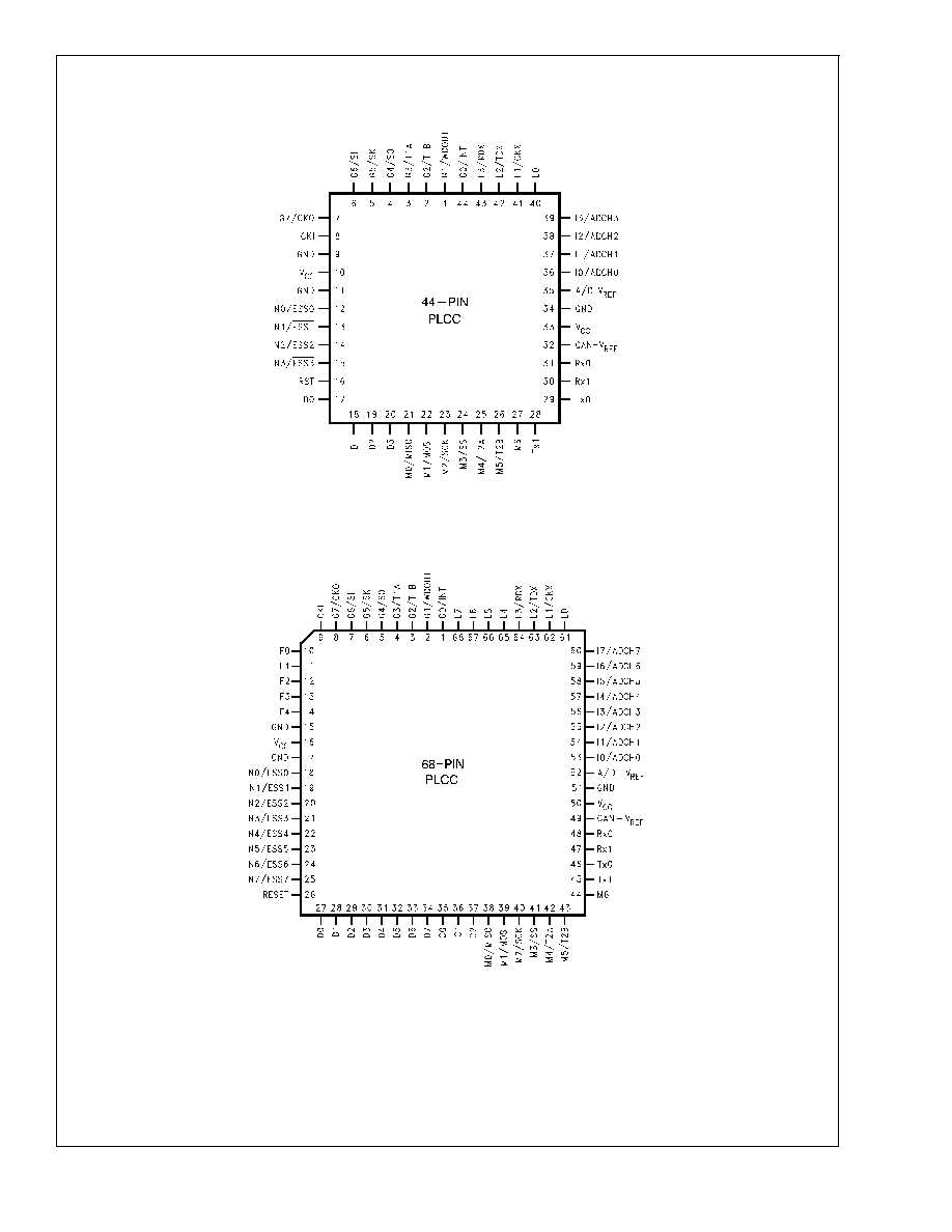
Devices included in this datasheet are:
Device
Memory (bytes)
RAM (bytes)
I/O Pins
Packages
Temperature
COP87L88EB
16k OTP EPROM
192
35
44 PLCC
-40 to +85∞C
COP87L89EB
16k OTP EPROM
192
58
68 PLCC
-40 to +85∞C
COP87L88RB
32k OTP EPROM
192
35
44 PLCC
-40 to +85∞C
COP87L89RB
32k OTP EPROM
192
58
68 PLCC
-40 to +85∞C
Key Features
n
CAN 2.0B (passive) bus interface, with Software Power
save mode
n
8-bit A/D Converter with 8 channels
n
Fully buffered USART
n
Multi-input wake up (MIWU) on both Port L and M
n
SPI Compatible Master/Slave Interface
n
16 or 32 kbytes of on-board OTP EPROM with security
feature
Note: Mask ROMed device with equivalent on-chip features and program
memory size of 8k is available.
n
192 bytes of on-board RAM
Additional Peripheral Features
n
Idle timer (programmable)
n
Two 16-bit timer, with two 16-bit registers supporting
-- Processor independent PWM mode
-- External Event counter mode
-- Input capture mode
n
WATCHDOG
TM
and Clock Monitor
n
MICROWIRE/PLUS serial I/O
I/O Features
n
Software selectable I/O options (TRI-STATE
Æ
outputs,
Push pull outputs, Weak pull up input, High impedance
input)
n
Schmitt trigger inputs on Port G, L and M
n
Packages: 44 PLCC with 35 I/O pins;
68 PLCC with 58 I/O pins
CPU/Instruction Set Features
n
1 µs instruction cycle time
n
Fourteen multi-sourced vectored interrupts servicing
-- External interrupt
-- Idle Timer T0
-- Timers (T1 and T2) (4 Interrupts)
-- MICROWIRE/PLUS and SPI
-- Multi-input Wake up
-- Software Trap
-- CAN interface (3 interrupts)
-- USART (2 Inputs)
n
Versatile easy to use instruction set
n
8-bit stacker pointer (SP) (Stack in RAM)
n
Two 8-bit RegisterR Indirect Memory Pointers (B, X)
Fully Static CMOS
n
Two power saving modes: HALT, IDLE
n
Single supply operation: 4.5V to 5.5V
n
Temperature range: -40∞C to +85∞C
Development Support
n
Emulation device for COP888EB
n
Real time emulation and full program debug offered by
MetaLink Development System
TRI-STATE
Æ
is a registered trademark of National Semiconductor Corporation.
COP8
TM
, MICROWIRE/PLUS
TM
, WATCHDOG
TM
and MICROWIRE
TM
are trademarks of National Semiconductor Corporation.
iceMASTER
Æ
is a registered trademark of MetaLink Corporation.
September 1999
COP87L88EB/RB
Family
,
8-Bit
CMOS
OTP
Microcontrollers
with
16k
or
32k
Memory
,
CAN
Interface,
8-Bit
A/D,
and
USART
© 2000 National Semiconductor Corporation
DS100044
www.national.com
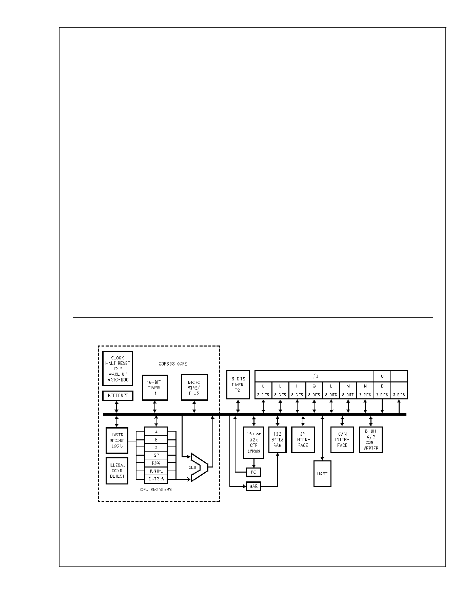
Basic Functional Description
n
CAN I/F -- CAN serial bus interface block as described
in the CAN specification part 2.0B (Passive)
-- Interface rates up to 250k bit/s are supported utilizing
standard message identifiers
n
Programmable double buffered USART
n
A/D -- 8-bit, 8 channel, 1-LSB Resolution, with improved
Source Impedance and improved channel to channel
cross talk immunity
n
Multi-Input-Wake-Up (MIWU) -- edge selectable wake-up
and interrupt capability via input port and CAN interface
(Port L, Port M and CAN I/F); supports Wake-Up
capability on SPI, USART, and T2
n
Port C -- 8-bit bi-directional I/O port
n
Port D -- 8-bit Output port with high current drive
capability (10 mA)
n
Port F -- 8-bit bidirectional I/O
n
Port G -- 8-bit bidirectional I/O port, including alternate
functions for:
-- MICROWIRE
TM
Input and Output
-- Timer 1 Input or Output (Depending on mode
selected)
-- External Interrupt input
-- WATCHDOG Output
n
Port I -- 8-bit input port combining either digital input, or
up to eight A/D input channels
n
Port L -- 8-bit bidirectional I/O port, including alternate
functions for:
-- USART Transmit/Receive I/O
-- Multi-input-wake up (MIWU on all pins)
n
Port M -- 8-bit I/O port, with the following alternate
function
-- SPI Interface
-- MIWU
-- CAN Interface Wake-up (MSB)
-- Timer 2 Input or Output (Depending on mode
selected)
n
Port N -- 8-bit bidirectional I/O
-- SPI Slave Select Expander
n
Two 16-bit multi-function Timer counters (T1 and T2)
plus supporting registers
-- (I/P Capture, PWM and Event Counting)
n
Idle timer -- Provides a basic time-base counter, (with
interrupt) and automatic wake up from IDLE mode
programmable
n
MICROWIRE/PLUS -- MICROWIRE serial peripheral
interface, supporting both Master and Slave operation
n
HALT and IDLE -- Software programmable low current
modes
-- HALT -- Processor stopped, Minimum current
-- IDLE -- Processor semi-active more than 60% power
saving
n
16 or 32 kbytes OTP EPROM and 192 bytes of on
board static RAM
n
SPI Master/Slave interface includes 12 bytes Transmit
and 12 bytes Receive FIFO Buffers. Operates up to 1M
Bit/S
n
On board programmable WATCHDOG and CLOCK
Monitor
Applications
n
Automobile Body Control and Comfort System
n
Integrated Driver Informaiton Systems
n
Steering Wheel Control
n
Car Radio Control Panel
n
Sensor/Actuator Applications in Automotive and
Industrial Control
Block Diagram
DS100044-1
FIGURE 1. Block Diagram
COP87L88RB/COP87L89RB
www.national.com
2
Absolute Maximum Ratings
(Note 1)
If Military/Aerospace specified devices are required,
please contact the National Semiconductor Sales Office/
Distributors for availability and specifications.
Supply Voltage (V
CC
)
6V
Voltage at Any Pin
-0.3V to V
CC
+0.3V
Total Current into V
CC
Pins (Source)
90 mA
Total Current out of GND Pins (Sink)
100 mA
Storage Temperature Range
-65∞C to +150∞C
Note 1: Absolute maximum ratings indicate limits beyond which damage to
the device may occur. DC and AC electrical specifications are not ensured
when operating the device at absolute maximum ratings.
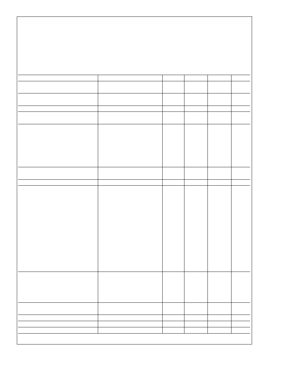
DC Electrical Characteristics
-40∞C
T
A
+85∞C
Parameter
Conditions
Min
Typ
Max
Units
Operating Voltage
4.5
5.5
V
Power Supply Ripple (Note 2)
Peak-to-Peak
0.1 V
CC
V
Supply Current
V
CC
= 5.5V, t
c
= 1 µs
16
mA
CKI = 10 MHz (Note 3)
HALT Current (Notes 4, 5)
V
CC
= 5.5V, CKI = 0 MHz
<
1
µA
IDLE Current (Note 5)
V
CC
= 5.5V, t
c
= 1 µs
5.5
mA
CKI = 10 MHz
Input Levels (V
IH
, V
IL
)
Reset, CKI
Logic High
0.8V
CC
V
Logic Low
0.2V
CC
V
All Other Inputs
Logic High
0.7V
CC
V
Logic Low
0.2V
CC
V
Hi-Z Input Leakage
V
CC
= 5.5V
±
2
µA
Input Pull-Up Current
V
CC
= 5.5V, V
IN
= 0V
-40
-250
µA
Port G, L and M Input Hysteresis
(Note 8)
0.05V
CC
V
Output Current Levels
D Outputs
Source
V
CC
= 4.5V, V
OH
= 3.3V
-0.4
mA
Sink
V
CC
= 4.5V, V
OL
= 1.0V
10
mA
CAN Transmitter Outputs
Source (Tx1)
V
CC
= 4.5V, V
OH
= V
CC
-0.1V
-1.5
mA
V
CC
= 4.5V, V
OH
= V
CC
- 0.6V
-10
+5.0
mA
Sink (Tx0)
V
CC
= 4.5V, V
OL
= 0.1V
1.5
mA
V
CC
= 4.5V, V
OL
= 0.6V
10
mA
All Others
Source (Weak Pull-Up)
V
CC
= 4.5V, V
OH
= 2.7V
-10
-110
µA
Source (Push-Pull)
V
CC
= 4.5V, V
OH
= 3.3V
-0.4
mA
Sink (Push-Pull)
V
CC
= 4.5V, V
OL
= 0.4V
1.6
mA
TRI-STATE Leakage
V
CC
= 5.5V
±
2.0
µA
Allowable Sink/Source Current per Pin
D Outputs (sink)
15
mA
Tx0 (Sink) (Note 8)
30
mA
Tx1 (Source) (Note 8)
30
mA
All Other
3
mA
Maximum Input Current
Room Temp
±
200
mA
without Latchup (Notes 6, 8)
RAM Retention Voltage, V
r
(Note 7)
500 ns Rise and Fall Time
2.0
V
Input Capacitance
(Note 8)
7
pF
Load Capacitance on D2
1000
pF
Note 2: Maxiumum rate of voltage change must be
<
0.5V/ms
COP87L88RB/COP87L89RB
www.national.com
5