TL DD12860
COP87L88RG
8-Bit
One-Time
Programmable
(OTP)
Microcontroller
with
32
Kbytes
of
Program
Memory
PRELIMINARY
September 1996
COP87L88RG
8-Bit One-Time Programmable (OTP) Microcontroller with
32 Kbytes of Program Memory
General Description
The COP87L88RG is a member of the COP8
TM
OTP micro-
controller family It is pin and software compatible to the
mask ROM COP888GG product family
(Continued)
Key Features
Y
Full duplex UART
Y
Three 16-bit timers each with two 16-bit registers
supporting
Processor independent PWM mode
External event counter mode
Input capture mode
Y
32 kbytes on-board EPROM with security feature
Note
Mask ROMed devices with equivalent on-chip features and pro-
gram memory sizes of 4k 8k 16k 20k and 24k are available (see
Table I)
Y
512 bytes on-board RAM
Additional Peripheral Features
Y
Idle timer
Y
Multi-Input Wake Up (MIWU) with optional interrupts (8)
Y
Two analog comparators
Y
WATCHDOG
TM
and clock monitor logic
Y
MICROWIRE PLUS
TM
serial I O
I O Features
Y
Memory mapped I O
Y
Software selectable I O options (TRI-STATE
output
push-pull output weak pull-up input high impedance in-
put
Y
Schmitt trigger inputs on ports G and L
Y
Packages
44 PLCC with 40 I O pins
40 DIP with 36 I O pins
CPU Instruction Set Features
Y
1 ms instruction cycle time
Y
Fourteen multi-source vectored interrupts servicing
External interrupt
Idle timer T0
Two timers (each with 2 interrupts)
MICROWIRE PLUS
Multi-Input Wake Up
Software trap
UART (2)
Default VIS (default interrupt)
Y
Versatile instruction set with true bit manipulation
Y
8-bit Stack Pointer SP (stack in RAM)
Y
Two
8-bit
register
indirect
data
memory
pointers
(B and X)
Fully Static CMOS
Y
Two power saving modes HALT and IDLE
Y
Single supply operation 2 7V ≠ 5 5V
Y
Temperature range
b
40 C to
a
85 C
Development Support
Y
Emulation device for the COP888EG COP888GG and
COP888HG
Y
Real time emulation and full program debug offered by
MetaLink Development System
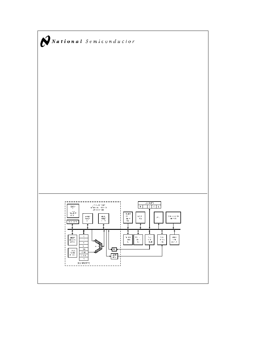
Block Diagram
TL DD12860 ≠ 1
FIGURE 1 Block Diagram
TRI-STATE
is a registered trademark of National Semiconductor Corporation
COP8
TM
MICROWIRE
TM
MICROWIRE PLUS
TM
and WATCHDOG
TM
are trademarks of National Semiconductor Corporation
iceMASTER
TM
is a trademark of MetaLink Corporation
C1996 National Semiconductor Corporation
RRD-B30M106 Printed in U S A
http
www national com
General Description
(Continued)
The device is a fully static part fabricated using double-met-
al silicon gate microCMOS technology Features include an
8-bit memory mapped architecture MICROWIRE PLUS
TM
serial I O three 16-bit timer counters supporting three
modes (Processor Independent PWM generation External
Event counter and Input Capture mode capabilities) full du-
plex UART and two comparators Each I O pin has software
selectable configurations The devices operates over a volt-
age range of 2 7V to 5 5V High throughput is achieved with
an efficient regular instruction set operating at a maximum
rate of 1 ms per instruction
TABLE I COP888CG EG GG HG Family Members
ROM EPROM
RAM
Key
Device
(Bytes)
(Bytes)
Common
Features
COP888CG
4k ROM
192
3 Timers
COP888EG
8k ROM
256
UART
COP888GG
16k ROM
512
2 Comparators
COP87L88GG 16k OTP EPROM
512
COP888HG
20k ROM
512
COP87L88RG 32k OTP EPROM
512
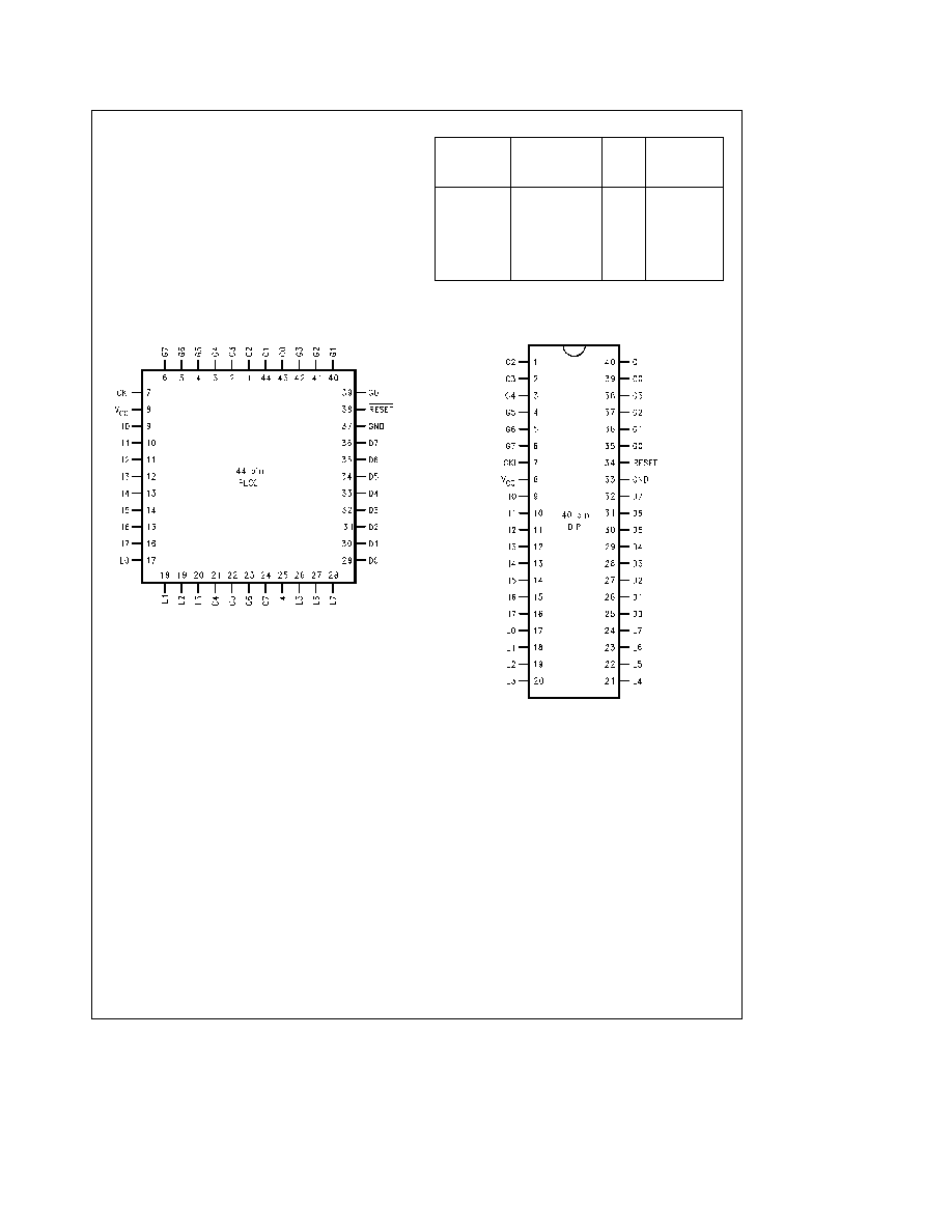
Connection Diagrams
Plastic Chip Carrier
TL DD12860 ≠ 2
Top View
Order Number COP87L88RGV-XE
See NS Package Number V44A
Note
-X
Crystal Oscillator
-E
Halt Enable
Dual-In-Line Package
TL DD12860 ≠ 3
Top View
Order Number COP87L88RGN-XE
See NS Package Number N40A
FIGURE 2 Connection Diagrams
http
www national com
2
Connection Diagrams
(Continued)
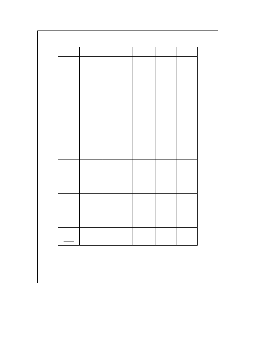
Pinouts for 40- and 44-Pin Packages
Port
Type
Alt Fun
Alt Fun
40-Pin
44-Pin
DIP
PLCC
L0
I O
MIWU
17
17
L1
I O
MIWU
CKX
18
18
L2
I O
MIWU
TDX
19
19
L3
I O
MIWU
RDX
20
20
L4
I O
MIWU
T2A
21
25
L5
I O
MIWU
T2B
22
26
L6
I O
MIWU
T3A
23
27
L7
I O
MIWU
T3B
24
28
G0
I O
INT
35
39
G1
WDOUT
36
40
G2
I O
T1B
37
41
G3
I O
T1A
38
42
G4
I O
SO
3
3
G5
I O
SK
4
4
G6
I
SI
5
5
G7
I CKO
HALT Restart
6
6
D0
O
25
29
D1
O
26
30
D2
O
27
31
D3
O
28
32
D4
O
29
33
D5
O
30
34
D6
O
31
35
D7
O
32
36
I0
I
9
9
I1
I
COMP1IN
b
10
10
I2
I
COMP1IN
a
11
11
I3
I
COMP1OUT
12
12
I4
I
COMP2IN
b
13
13
I5
I
COMP2IN
a
14
14
I6
I
COMP2OUT
15
15
I7
I
16
16
C0
I O
39
43
C1
I O
40
44
C2
I O
1
1
C3
I O
2
2
C4
I O
21
C5
I O
22
C6
I O
23
C7
I O
24
V
CC
8
8
GND
33
37
CKI
7
7
RESET
34
38
http
www national com
3
Absolute Maximum Ratings
(Note)
If Military Aerospace specified devices are required
please contact the National Semiconductor Sales
Office Distributors for availability and specifications
Supply Voltage (V
CC
)
7V
Voltage at Any Pin
b
0 3V to V
CC
a
0 3V
Total Current into V
CC
Pin (Source)
100 mA
Total Current out of GND Pin (Sink)
110 mA
Storage Temperature Range
b
65 C to
a
140 C
Note
Absolute maximum ratings indicate limits beyond
which damage to the device may occur DC and AC electri-
cal specifications are not ensured when operating the de-
vice at absolute maximum ratings
DC Electrical Characteristics
b
40 C
s
T
A
s
a
85 C unless otherwise specified
Parameter
Conditions
Min
Typ
Max
Units
Operating Voltage
2 7
5 5
V
Power Supply Ripple (Note 1)
Peak-to-Peak
0 1 V
CC
V
Supply Current (Note 2)
CKI
e
10 MHz
V
CC
e
5 5V t
c
e
1 ms
16 5
mA
CKI
e
4 MHz
V
CC
e
4 0V t
c
e
2 5 ms
6 5
mA
HALT Current (Note 3)
V
CC
e
5 5V CKI
e
0 MHz
12
m
A
V
CC
e
4 0V CKI
e
0 MHz
8
m
A
IDLE Current
CKI
e
10 MHz
V
CC
e
5 5V t
c
e
1 ms
3 5
mA
CKI
e
1 MHz
V
CC
e
4 0V t
c
e
10 ms
0 7
mA
Input Levels
RESET
Logic High
0 8 V
CC
V
Logic Low
0 2 V
CC
V
CKI (External and Crystal Osc Modes)
Logic High
0 7 V
CC
V
Logic Low
0 2 V
CC
V
All Other Inputs
Logic High
0 7 V
CC
V
Logic Low
0 2 V
CC
V
Hi-Z Input Leakage
V
CC
e
5 5V
b
2
a
2
m
A
Input Pullup Current
V
CC
e
5 5V
40
250
m
A
G and L Port Input Hysteresis
0 05 V
CC
0 35 V
CC
V
Output Current Levels
D Outputs
Source
V
CC
e
4 5V V
OH
e
3 3V
0 4
mA
Sink (Note 4)
V
CC
e
4 5V V
OL
e
1V
10
mA
All Others
Source (Weak Pull-Up Mode)
V
CC
e
4 5V V
OH
e
2 7V
10
100
m
A
Source (Push-Pull Mode)
V
CC
e
4 5V V
OH
e
3 3V
0 4
mA
Sink (Push-Pull Mode)
V
CC
e
4 5V V
OL
e
0 4V
1 6
mA
TRI-STATE Leakage
V
CC
e
5 5V
b
2
a
2
m
A
Allowable Sink Source
Current per Pin
D Outputs (Sink)
15
mA
All others
3
mA
Maximum Input Current
T
A
e
25 C
g
100
mA
without Latchup (Note 5)
RAM Retention Voltage V
r
500 ns Rise and Fall Time (Min)
2
V
Input Capacitance
7
pF
Load Capacitance on D2
1000
pF
Note 1
Rate of voltage change must be less then 0 5 V ms
Note 2
Supply current is measured after running 2000 cycles with a square wave CKI input CKO open inputs at rails and outputs open
Note 3
The HALT mode will stop CKI from oscillating in the RC and the Crystal configurations by bringing CKI high Test conditions All inputs tied to V
CC
L and G
ports in the TRI-STATE mode and tied to ground all outputs low and tied to ground The clock monitor is disabled
Note 4
The user must guarantee that D2 pin does not source more than 10 mA during RESET If D2 sources more than 10 mA during reset the device will go into
programming mode
Note 5
Pins G6 and RESET are designed with a high voltage input network for factory testing These pins allow input voltages greater than V
CC
and the pins will
have sink current to V
CC
when biased at voltages greater than V
CC
(the pins do not have source current when biased at a voltage below V
CC
) The effective
resistance to V
CC
is 750X (typical) These two pins will not latch up The voltage at the pins must be limited to less than 14V
http
www national com
4
AC Electrical Characteristics
b
40 C
s
T
A
s
a
85 C unless otherwise specified
Parameter
Conditions
Min
Typ
Max
Units
Instruction Cycle Time (t
c
)
Crystal Resonator
1
DC
m
s
R C Oscillator
3
DC
m
s
Inputs
t
SETUP
200
ns
t
HOLD
60
ns
Output Propagation Delay
R
L
e
2 2k C
L
e
100 pF
t
PD1
t
PD0
SO SK
0 7
m
s
All Others
1
m
s
MICROWIRE
TM
Setup Time (t
UWS
)
20
ns
MICROWIRE Hold Time (t
UWH
)
56
ns
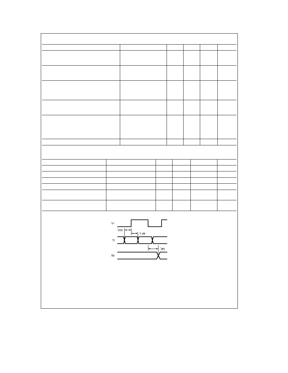
MICROWIRE Output Propagation Delay (t
UPD
)
220
ns
Input Pulse Width
Interrupt Input High Time
1
t
c
Interrupt Input Low Time
1
t
c
Timer Input High Time
1
t
c
Timer Input Low Time
1
t
c
Reset Pulse Width
1
m
s
Comparators AC and DC Characteristics
V
CC
e
5V T
A
e
25 C
Parameter
Conditions
Min
Typ
Max
Units
Input Offset Voltage
0 4V
s
V
IN
s
V
CC
b
1 5V
g
10
g
25
mV
Input Common Mode Voltage Range
0 4
V
CC
b
1 5
V
Low Level Output Current
V
OL
e
0 4V
1 6
mA
High Level Output Current
V
OH
e
4 6V
1 6
mA
DC Supply Current Per Comparator
250
m
A
(When Enabled)
Response Time
TBD mV Step TBD mV
1
m
s
Overdrive 100 pF Load
TL DD12860 ≠ 5
FIGURE 3 MICROWIRE PLUS Timing
http
www national com
5