COP87L88EK/RK Family
8-Bit CMOS OTP Microcontrollers with 8k or 32k
Memory, Comparator, and Single-slope A/D Capability
General Description
The COP87L88EK/RK Family OTP (One Time Program-
mable) microcontrollers are highly integrated COP8
TM
Fea-
ture core devices with 16k or 32k memory and advanced
features
including
a
Multi-Input
Comparator
and
Single-slope A/D capability. These multi-chip CMOS devices
are suited for applications requiring a full featured, low EMI
controller with an analog comparator, current source, and
voltage reference, and as pre-production devices for a
masked ROM design. Lower cost pin and software compat-
ible 8k ROM versions (COP888EK) are available for use with
a range of COP8 software and hardware development tools.
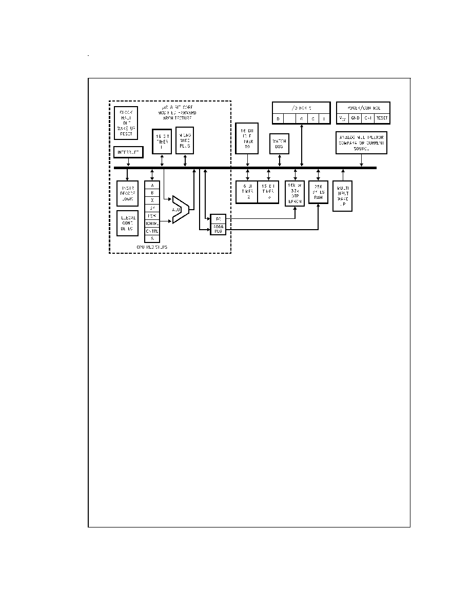
Family features include an 8-bit memory mapped architec-
ture, 10 MHz CKI (-XE = crystal oscillator) with 1 µs instruc-
tion cycle, three multi-function 16-bit timer/counters with
PWM, MICROWIRE/PLUS
TM
serial I/O, one analog com-
parator with seven input multiplexor, an analog current
source and V
CC
/2 reference, two power saving HALT/IDLE
modes, idle timer, MIWU, high current outputs, software se-
lectable I/O options, WATCHDOG
TM
timer and Clock Monitor,
2.7V to 5.5V operation and 28/40/44 pin packages.
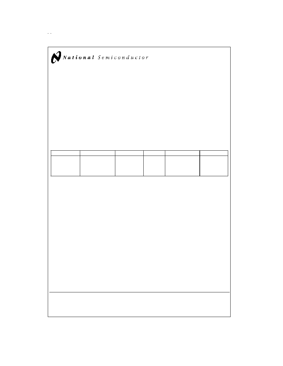
Devices included in this datasheet are:
Device
Memory (bytes)
RAM (bytes)
I/O Pins
Packages
Temperature
COP87L84EK
16k OTP EPROM
256
24
28 DIP/SOIC
-40 to +85∞C
COP87L88EK
16k OTP EPROM
256
36/40
40 DIP, 44 PLCC
-40 to +85∞C
COP87L84RK
32k OTP EPROM
256
24
28 DIP/SOIC
-40 to +85∞C
COP87L88RK
32k OTP EPROM
256
36/40
40 DIP, 44 PLCC
-40 to +85∞C
Key Features
n
Analog function block with
-- Analog comparator with seven input multiplexor
-- Constant current source and V
CC
/2 reference
n
Three 16-bit timers, each with two 16-bit registers
supporting:
-- Processor Independent PWM mode
-- External Event counter mode
-- Input Capture mode
n
8 or 32 kbytes on-board EPROM with security feature
n
256 bytes on-board RAM
Additional Peripheral Features
n
Idle Timer
n
Multi-Input Wake Up (MIWU) with optional interrupts (8)
n
WATCHDOG and Clock Monitor logic
n
MICROWIRE/PLUS serial I/O
I/O Features
n
Software selectable I/O options ( TRI-STATE
TM
Output,
Push-Pull Output, Weak Pull-Up Input, High Impedance
Input)
n
Packages:
-- 44 PLCC with 40 I/O pins
-- 40 DIP with 36 I/O pins
-- 28 DIP/SO with 24 I/O pins
n
Schmitt trigger inputs on Port G and L
CPU/Instruction Set Feature
n
1 µs instruction cycle time
n
Twelve multi-source vectored interrupts servicing
-- External Interrupt with selectable edge
-- Idle Timer T0
-- Three Timers (Each with 2 interrupts)
-- MICROWIRE/PLUS
-- Multi-Input Wake Up
-- Software Trap
-- Default VIS (default interrupt)
n
Versatile and easy to use instruction set
n
8-bit Stack Pointer (SP) -- stack in RAM
n
Two 8-bit Register Indirect Data Memory Pointers
(B, X)
Fully Static CMOS
n
Two power saving modes: HALT and IDLE
n
Single supply operation: 2.7V to 5.5V
n
Temperature ranges: -40∞C to +85∞C
Development Support
n
Emulation devices for the COP888EK/COP884EK
n
Real time emulation and full program debug offered by
MetaLink Development System
COP8
TM
is a trademark of National Semiconductor Corporation.
MICROWIRE/PLUS
TM
is a trademark of National Semiconductor Corporation.
TRI-STATE
Æ
is a registered trademark of National Semiconductor Corporation.
WATCHDOG
TM
is a trademark of National Semiconductor Corporation.
iceMASTER
TM
is a trademark of MetaLink Corporation.
September 1999
COP87L88EK/RK
Family,
8-Bit
CMOS
OTP
Microcontrollers
with
8k
or
32k
Memory
,
Comparator
,
and
Single-slope
A/D
Capability
© 1999 National Semiconductor Corporation
DS101133
www.national.com
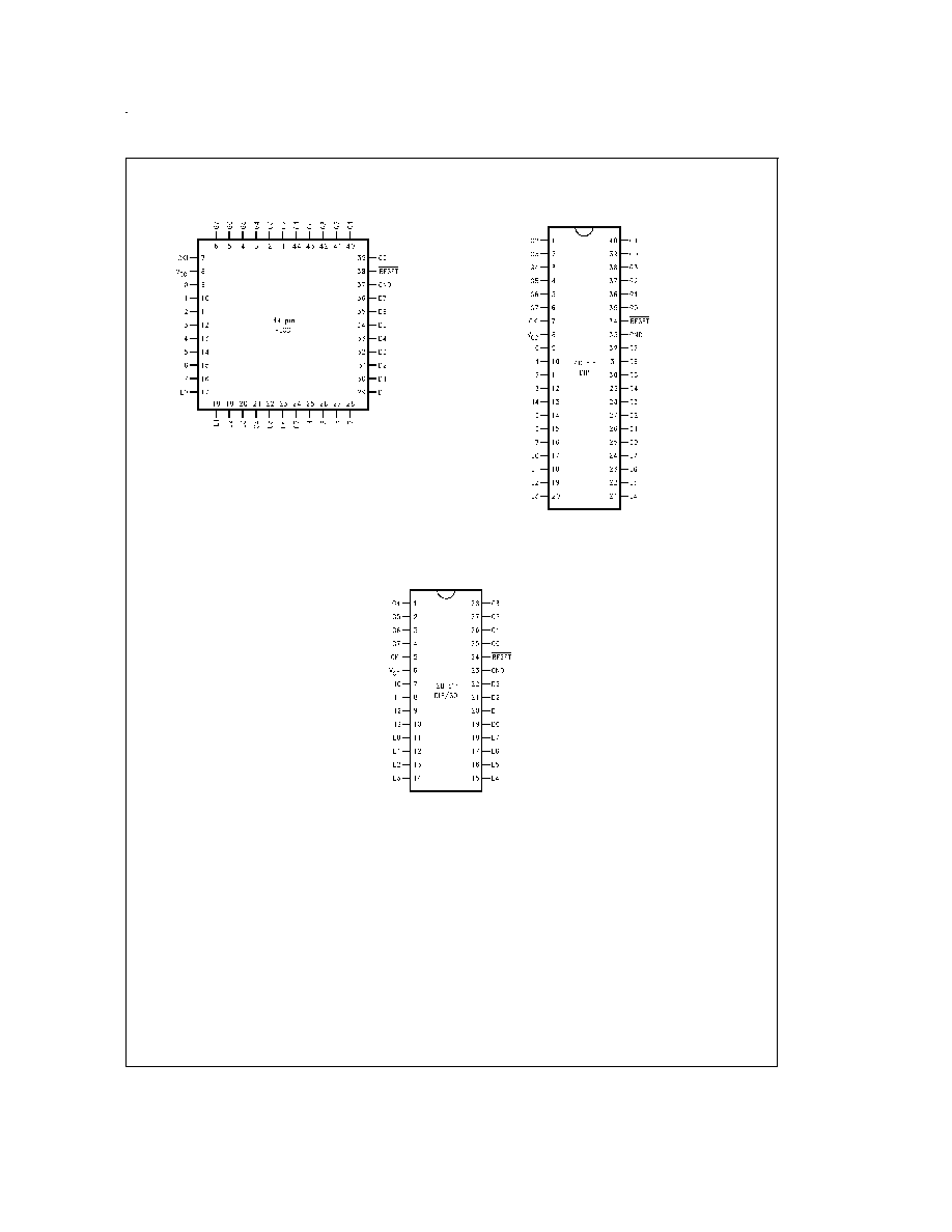
Connection Diagrams
Plastic Chip Carrier
DS101133-2
Top View
Order Number COP87L88EKV-XE or COP87L88RKV-XE
See NS Plastic Chip Package Number V44A
Dual-In-Line Package
DS101133-3
Top View
Order Number COP87L84EKN-XE or COP87L84RKN-XE
See NS Molded Package Number N40A
Dual-In-Line Package
DS101133-4
Top View
Order Number COP87L84EKN-XE or COP87L84RKN-XE
See NS Molded Package Number N28B
Order Number COP87L84EKM-XE or COP87L84RKM-XE
See NS Molded Package Number M28B
Note: -X Crystal Oscillator
-E Halt Mode Enabled
FIGURE 2. Connection Diagrams
www.national.com
3
Absolute Maximum Ratings
(Note 1)
If Military/Aerospace specified devices are required,
please contact the National Semiconductor Sales Office/
Distributors for availability and specifications.
Supply Voltage (V
CC
)
7V
Voltage at Any Pin
-0.3V to V
CC
+ 0.3V
Total Current into V
CC
Pin (Source)
100 mA
Total Current out of GND Pin (Sink)
110 mA
Storage Temperature Range
-65∞C to +140∞C
Note 1:
Absolute maximum ratings indicate limits beyond which damage to
the device may occur. DC and AC electrical specifications are not ensured
when operating the device at absolute maximum ratings.
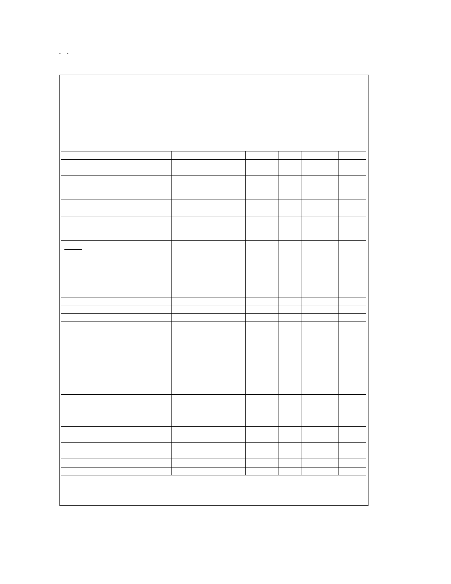
DC Electrical Characteristics
-40∞C
T
A
+85∞C unless otherwise specified
Parameter
Conditions
Min
Typ
Max
Units
Operating Voltage
2.7
5.5
V
Power Supply Ripple (Note 3)
Peak-to-Peak
0.1 V
CC
V
Supply Current (Note 4)
CKI = 10 MHz
V
CC
= 5.5V, t
c
= 1 µs
16.5
mA
CKI = 4 MHz
V
CC
= 4.0V, t
c
= 2.5 µs
6.5
mA
HALT Current (Note 5)
V
CC
= 5.5V, CKI = 0 MHz
12
µA
V
CC
= 4.0V, CKI = 0 MHz
8
µA
IDLE Current (Note 4)
CKI = 10 MHz
V
CC
= 5.5V, t
c
= 1 µs
3.5
mA
CKI = 4 MHz
V
CC
= 4.0V, t
c
= 10 µs
0.7
mA
Input Levels (V
IH
, V
IL
)
RESET
Logic High
0.8 V
CC
V
Logic Low
0.2 V
CC
V
CKI, All Other Inputs
Logic High
0.7 V
CC
V
Logic Low
0.2 V
CC
V
Hi-Z Input Leakage
V
CC
= 5.5V
-2
+2
µA
Input Pullup Current
V
CC
= 5.5V, V
IN
= 0V
-40
-250
µA
G and L Port Input Hysteresis (Note 8)
0.35 V
CC
V
Output Current Levels
D Outputs
Source
V
CC
= 4.5V, V
OH
= 3.3V
-0.4
mA
Sink
V
CC
= 4.5V, V
OL
= 1V
10
mA
All Others
Source (Weak Pull-Up Mode)
V
CC
= 4.5V, V
OH
= 2.7V
-10
-110
µA
Source (Push-Pull Mode)
V
CC
= 4.5V, V
OH
= 3.3V
-0.4
mA
Sink (Push-Pull Mode)
V
CC
= 4.5V, V
OL
= 0.4V
1.6
mA
TRI-STATE Leakage
V
CC
= 6.0V
-2
+2
µA
Allowable Sink/Source Current per Pin
(Note 8)
D Outputs (Sink)
15
mA
All others
3
mA
Maximum Input Current
Room Temp
±
200
mA
without Latchup (Note 6)
RAM Retention Voltage, V
r
500 ns Rise
2
V
and Fall Time (min)
Input Capacitance
7
pF
Load Capacitance on D2
1000
pF
www.national.com
5