TL DD12855
COP87L88RW
8-Bit
One-Time
Programmable
(OTP)
Microcontroller
with
Pulse
Train
Generators
and
Capture
Modules
PRELIMINARY
September 1996
COP87L88RW
8-Bit One-Time Programmable (OTP) Microcontroller
with Pulse Train Generators and Capture Modules
General Description
The COP87L88RW is a member of the COP8
TM
8-bit OTP
microcontroller family It is pin and software compatible to
the mask ROM COP888GW product family
(Continued)
Key Features
Y
Multiply divide functions
Y
Full duplex UART
Y
Four pulse train generators with 16-bit prescalers
Y
Two 16-bit input capture modules with 8-bit prescalers
Y
Two 16-bit timers each with two 16-bit registers
supporting
Processor independent PWM mode
External event counter mode
Input capture mode
Y
32 kbytes on-board OTP EPROM with security feature
Note
Mask ROMed devices with equivalent on-chip features and program
memory sizes of 16k is available
Y
512 bytes on-board RAM
Additional Peripheral Features
Y
Idle Timer
Y
Multi-Input Wake-Up (MIWU) with optional interrupts (8)
Y
WATCHDOG
TM
and clock monitor logic
Y
MICROWIRE PLUS
TM
serial I O
I O Features
Y
Memory mapped I O
Y
Software selectable I O options
TRI-STATE
output
Push-pull output
Weak pull-up input
High impedance input
Y
Schmitt trigger inputs on ports G and L
Y
Package
68 PLCC with I O pins
CPU Instruction Set Features
Y
1 ms instruction cycle time
Y
Fourteen multi-source vectored interrupts servicing
External interrupt
Idle timer T0
Two timers (each with 2 interrupts)
MICROWIRE PLUS
Multi-Input Wake-Up
Software trap
UART (2)
Default VIS
Capture timers
Counters (one vector for all four counters)
Y
Versatile and easy to use instruction set
Y
8-bit Stack Pointer (SP)
stack in RAM
Y
Two 8-bit register indirect data memory pointers
(B and X)
Fully Static CMOS
Y
Two power saving modes HALT and IDLE
Y
Single supply operation 2 7V to 5 5V
Y
Temperature range
b
40 C to
a
85 C
Development Support
Y
Emulation device for the COP888GW
Y
Real time emulation and full program debug offered by
MetaLink's Development System
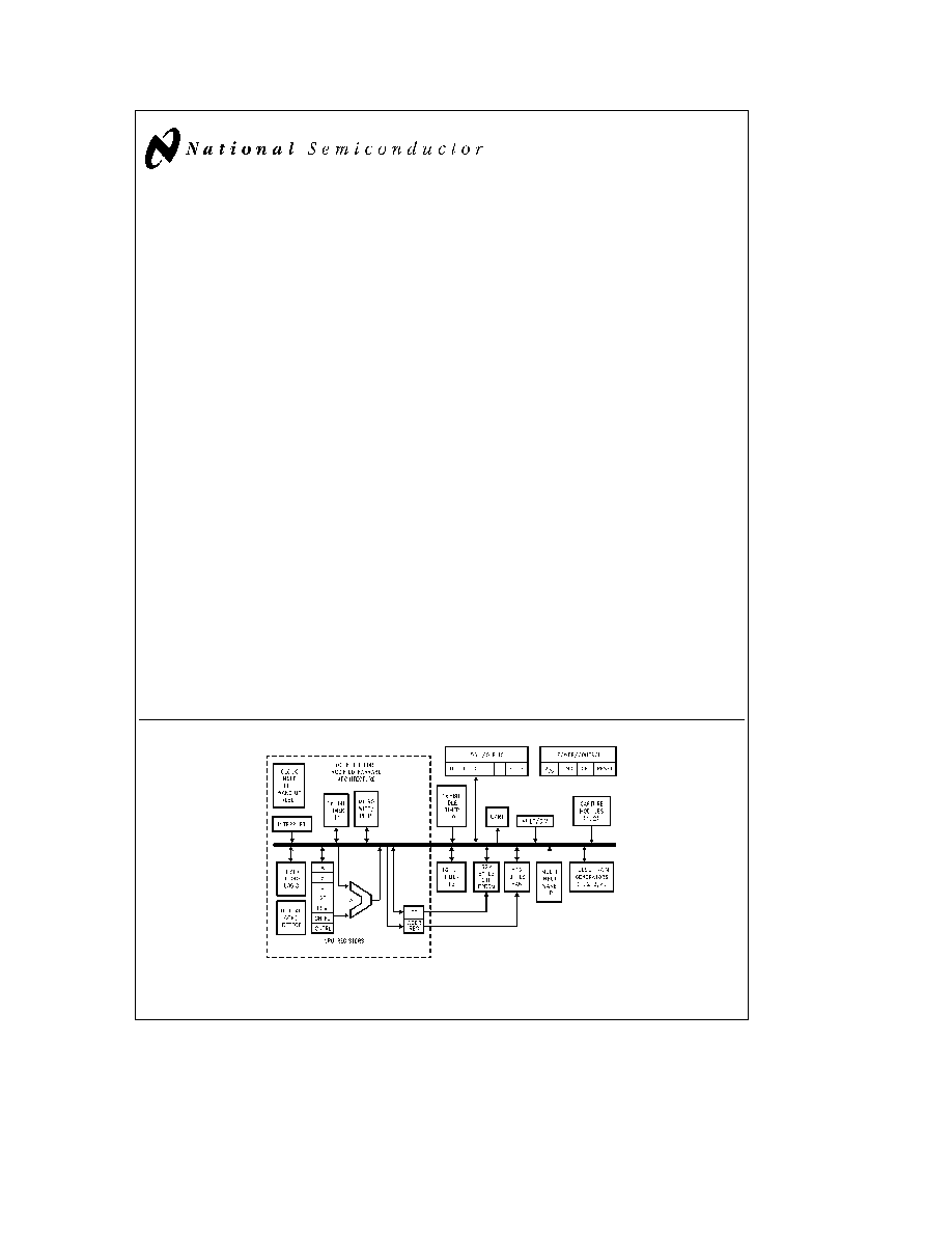
Block Diagram
TL DD 12855 ≠ 1
FIGURE 1 COP87L88RW Block Diagram
TRI-STATE
is a registered trademark of National Semiconductor Corporation
MICROWIRE PLUS
TM
COPS
TM
microcontrollers MICROWIRE
TM
WATCHDOG
TM
and COP8
TM
are trademarks of National Semiconductor Corporation
iceMASTER
TM
is a trademark of MetaLink Corporation
C1996 National Semiconductor Corporation
RRD-B30M106 Printed in U S A
http
www national com
General Description
(Continued)
It is a fully static part fabricated using double-metal silicon
gate microCMOS technology Features include an 8-bit
memory mapped architecture MICROWIRE PLUS serial
I O two 16-bit timer counters supporting three modes
(Processor Independent PWM generation External Event
counter and Input Capture mode capabilities) four indepen-
dent 16-bit pulse train generators with 16-bit prescalers two
independent 16-bit input capture modules with 8-bit prescal-
ers multiply and divide functions full duplex UART and two
power savings modes (HALT and IDLE) both with a mul-
ti-sourced wake up interrupt capability This multi-sourced
interrupt capability may also be used independent of the
HALT or IDLE modes Each I O pin has software selectable
configurations The devices operate over a voltage range of
2 7V--5 5V High throughput is achieved with an efficient
regular instruction set operating at a maximum of 1 ms per
instruction rate
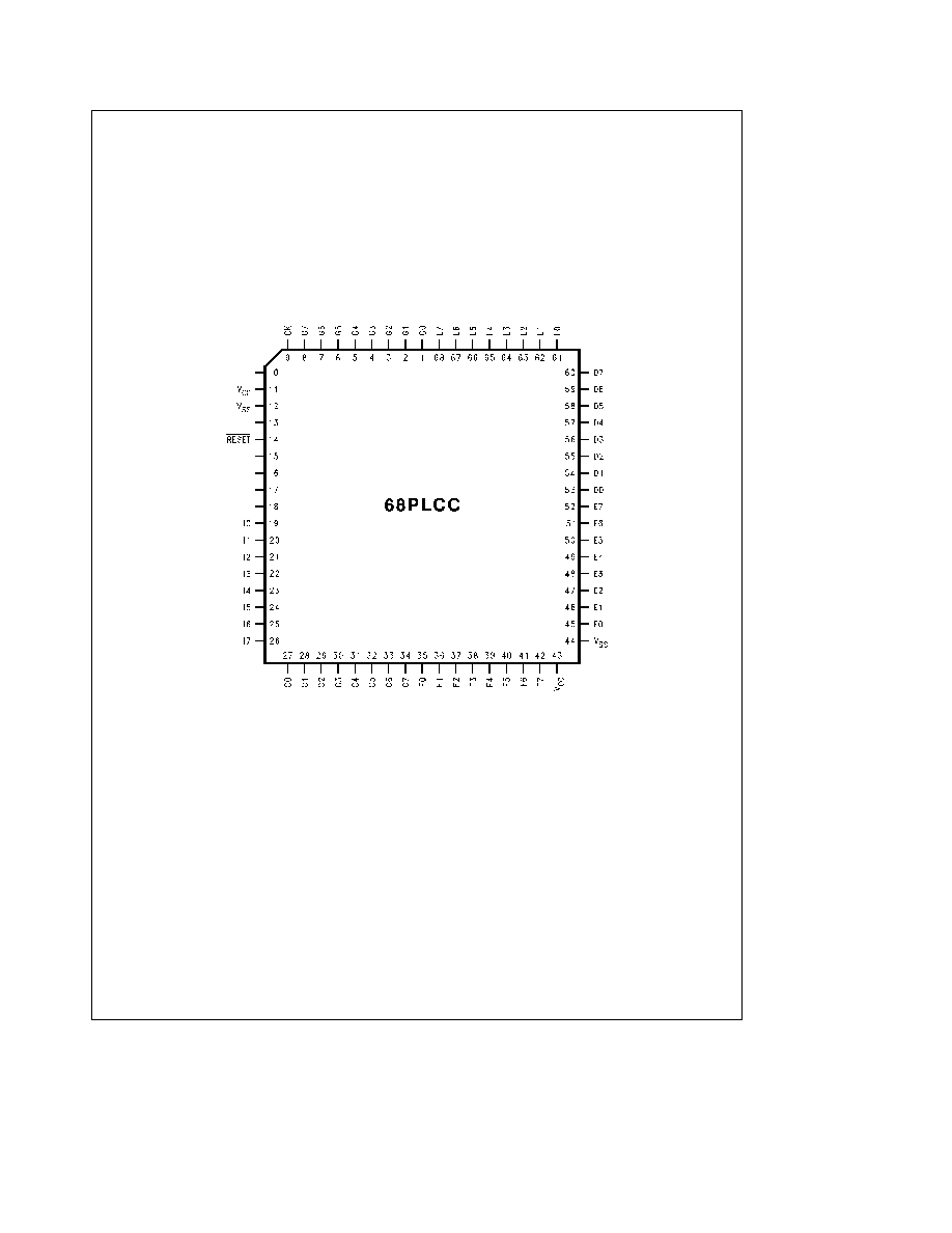
Connection Diagram
TL DD 12855 ≠ 2
Top View
Note
-X Crystal Oscillator
-E Halt Enable
Order Number COP87L88RWV-XE
See NS Plastic Chip Package Number V68A
FIGURE 2 Connection Diagram
http
www national com
2
Absolute Maximum Ratings
(Note)
SuppIy Voltage (V
CC
)
7V
Voltage at Any Pin
b
0 3V to V
CC
a
0 3V
Total Current into V
CC
Pin (Source)
100 mA
Total Current out of GND Pin (Sink)
110 mA
Storage Temperature Range
b
65 C to
a
150 C
Note
Absolute maximum ratings indicate limits beyond
which damage to the device may occur DC and AC electri-
cal specifications are not ensured when operating the de-
vice at absolute maximum ratings
DC Electrical Characteristics
b
40 C
s
T
A
s
a
85 C unless otherwise specified
Parameter
ConditIons
Min
Typ
Max
UnIts
Operating Voltage
2 7
5 5
V
Power Supply Ripple (Note 1)
Peak-to-Peak
0 1 V
CC
V
Supply Current (Note 2)
CKI
e
10 MHz
V
CC
e
5 5V t
c
e
1 ms
14
mA
HALT Current (Note 3)
V
CC
e
5 5V CKI
e
0 MHz
12
m
A
IDLE Current
CKI
e
10 MHz
V
CC
e
5 5V
1 7
mA
Input Levels (V
IH
V
IL
)
RESET CKI
Logic High
0 8 V
CC
V
Logic Low
0 2 V
CC
V
All Other Inputs
Logic High
0 7 V
CC
V
Logic Low
0 2 V
CC
V
Hi-Z Input Leakage
V
CC
e
5 5V
b
2
a
2
m
A
Input Pullup Current
V
CC
e
5 5V V
IN
e
0V
40
b
250
m
A
G Port Input Hysteresis
(Note 6)
0 05 V
CC
0 35 V
CC
V
Output Current Levels
D Outputs
Source
V
CC
e
4 5V V
OH
e
3 3V
b
0 4
mA
Sink (Note 4)
V
CC
e
4 5V V
OL
e
1V
10
mA
All Others
Source (Weak Pull-Up Mode)
V
CC
e
4 5V V
OH
e
2 7V
b
10
b
100
m
A
Source (Push-Pull Mode)
V
CC
e
4 5V V
OH
e
3 3V
b
0 4
mA
Sink (Push-Pull Mode)
V
CC
e
4 5V V
OL
e
0 4V
1 6
mA
TRI-STATE Leakage
V
CC
e
5 5V
b
2
a
2
m
A
Allowable Sink Source
Current per Pin
D Outputs (Sink)
15
mA
All others
3
mA
Maximum Input Current
Room Temp
g
200
mA
without Latchup (Note 5 7)
RAM Retention Voltage V
r
(Note 6)
500 ns Rise and Fall Time (min)
2
V
Input Capacitance
(Note 7)
7
pF
Load Capacitance on D2
(Note 7)
1000
pF
http
www national com
3
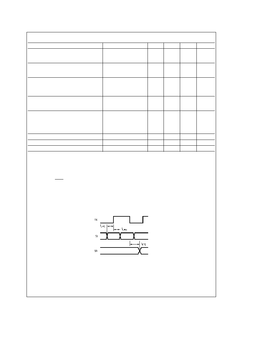
AC Electrical Characteristics
b
40 C
s
T
A
s
a
85 C unless otherwise specified
Parameter
Conditions
Min
Typ
Max
Units
Instruction Cycle Time (t
c
)
Crystal Resonator
1 0
DC
m
s
Ceramic
Inputs
t
SETUP
V
CC
t
4 5V
200
ns
t
HOLD
V
CC
t
4 5V
60
ns
Output Propagation Delay (Note 9)
R
L
e
2 2k C
L
e
100 pF
t
PD1
t
PD0
SO SK
V
CC
t
4 5V
0 7
m
s
All Others
V
CC
t
4 5V
1
m
s
MICROWIRE
TM
Setup Time (t
UWS
) (Note 7)
V
CC
t
4 5V
20
MICROWIRE Hold Time (t
UWH
) (Note 7)
V
CC
t
4 5V
56
ns
MICROWIRE Output Propagation Delay (t
UPD
)
V
CC
t
4 5V
220
Input Pulse Width (Note 8)
Interrupt Input High Time
1
Interrupt Input Low Time
1
t
c
Timer 1 2 Input High Time
1
Timer 1 2 Input Low Time
1
Capture Timer High Time
1
CKI
Capture Timer Low Time
1
CKI
Reset Pause Width
1
m
s
Note 1
Maximum rate of voltage change to be defined
Note 2
Supply current is measured after running 2000 cydes with a square wave CKI input CKO open inputs at rails and outputs open
Note 3
The HALT mode will stop CKI from oscillatng Test conditions All inputs tied to V
CC
L C E F and G port I O's configured as outputs and programmed
low and not driving a load D outputs programmed low and not driving a load Parameter refers to HALT mode entered via setting bit 7 of the G Port data register
Part will pull up CKI during HALT in crystal clock mode
Note 4
The user must guarantee that D2 pin does not source more than 10 mA during RESET If D2 sources more than 10 mA during reset the device will go into
programming mode
Note 5
Pins G6 and RESET are designed with a high voltage input network These pins allow input voltages greater than V
CC
and the pins will have sink current to
V
CC
when biased at voltages greater than V
CC
(the pins do not have source current when biased at a voltage below V
CC
) The effective resistance to V
CC
is 750X
(typical) These two pins will not latch up The voltage at the pins must be limited to less than 14V WARNING Voltages in excess of 14V will cause damage to the
pins This warning excludes ESD transients
Note 6
Condition and parameter valid only for part in HALT mode
Note 7
Parameter characterized but not tested
Note 8
t
c
e
Instruction Cycle Time
Note 9
The output propagation delay is referenced to the end of the instruction cycle where the output change occurs
TL DD 12855 ≠ 3
FIGURE 3 MICROWIRE PLUS Timing
http
www national com
4
Pin Descriptions
V
CC
and GND are the power supply pins All V
CC
and GND
pins must be connected
CKI is the clock input This comes from a crystal oscillator
(in conjunction with CKO) See Oscillator Description sec-
tion
RESET is the master reset input See Reset description
section
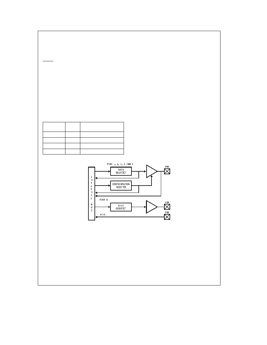
The device contains five bidirectional 8-bit I O ports (C E
F G and L) where each individual bit may be independently
configured as an input (Schmitt trigger inputs on ports L and
G) output or TRI-STATE under program control Three data
memory address locations are allocated for each of these
I O ports Each I O port has two associated 8-bit memory
mapped registers the CONFIGURATION register and the
output DATA register A memory mapped address is also
reserved for the input pins of each I O port (See the memo-
ry map for the various addresses associated with the I O
ports )
Figure 4 shows the I O port configurations The
DATA and CONFIGURATION registers allow for each port
bit to be individually configured under software control as
shown below
Configuration
Data
Port Set-Up
Register
Register
0
0
Hi-Z Input (TRI-STATE Output)
0
1
Input with Weak Pull-Up
1
0
Push-Pull Zero Output
1
1
Push-Pull One Output
PORT L is an 8-bit I O port All L-pins have Schmitt triggers
on the inputs
The Port L supports Multi-Input Wake Up on all eight pins
L1 is used for the UART external clock L2 and L3 are used
for the UART transmit and receive L4 and L5 are used for
the timer input functions T2A and T2B L6 and L7 are used
for the capture timer input functions CAP1 and CAP2
The Port L has the following alternate features
L0
MIWU
L1
MIWU or CKX
L2
MIWU or TDX
L3
MIWU or RDX
L4
MIWU or T2A
L5
MIWU or T2B
L6
MIWU or CAP1
L7
MIWU or CAP2
Port G is an 8-bit port with 6 I O pins (G0 ≠ G5) an input pin
(G6) and a dedicated output pin (G7) Pins G0 ≠ G6 all have
Schmitt Triggers on their inputs Pin G7 serves as the dedi-
cated output pin for the CKO clock output There are two
registers associated with the G Port a data register and a
configuration register Therefore each of the 6 I O bits
(G0 ≠ G5) can be individually configured under software con-
trol
TL DD 12855 ≠ 4
FIGURE 4 I O Port Configurations
http
www national com
5